EP0603600A2 - Compensation du retard de trajet dans un système en bande ouverte - Google Patents
Compensation du retard de trajet dans un système en bande ouverte Download PDFInfo
- Publication number
- EP0603600A2 EP0603600A2 EP93119383A EP93119383A EP0603600A2 EP 0603600 A2 EP0603600 A2 EP 0603600A2 EP 93119383 A EP93119383 A EP 93119383A EP 93119383 A EP93119383 A EP 93119383A EP 0603600 A2 EP0603600 A2 EP 0603600A2
- Authority
- EP
- European Patent Office
- Prior art keywords
- timing signal
- data
- point
- synchronizing timing
- selectively adjusting
- Prior art date
- Legal status (The legal status is an assumption and is not a legal conclusion. Google has not performed a legal analysis and makes no representation as to the accuracy of the status listed.)
- Ceased
Links
Images



Classifications
-
- H—ELECTRICITY
- H04—ELECTRIC COMMUNICATION TECHNIQUE
- H04J—MULTIPLEX COMMUNICATION
- H04J3/00—Time-division multiplex systems
- H04J3/02—Details
- H04J3/06—Synchronising arrangements
- H04J3/0635—Clock or time synchronisation in a network
- H04J3/0682—Clock or time synchronisation in a network by delay compensation, e.g. by compensation of propagation delay or variations thereof, by ranging
-
- H—ELECTRICITY
- H04—ELECTRIC COMMUNICATION TECHNIQUE
- H04L—TRANSMISSION OF DIGITAL INFORMATION, e.g. TELEGRAPHIC COMMUNICATION
- H04L7/00—Arrangements for synchronising receiver with transmitter
- H04L7/0008—Synchronisation information channels, e.g. clock distribution lines
-
- H—ELECTRICITY
- H04—ELECTRIC COMMUNICATION TECHNIQUE
- H04L—TRANSMISSION OF DIGITAL INFORMATION, e.g. TELEGRAPHIC COMMUNICATION
- H04L7/00—Arrangements for synchronising receiver with transmitter
- H04L7/0016—Arrangements for synchronising receiver with transmitter correction of synchronization errors
- H04L7/0033—Correction by delay
- H04L7/0037—Delay of clock signal
-
- H—ELECTRICITY
- H04—ELECTRIC COMMUNICATION TECHNIQUE
- H04L—TRANSMISSION OF DIGITAL INFORMATION, e.g. TELEGRAPHIC COMMUNICATION
- H04L7/00—Arrangements for synchronising receiver with transmitter
- H04L7/02—Speed or phase control by the received code signals, the signals containing no special synchronisation information
- H04L7/033—Speed or phase control by the received code signals, the signals containing no special synchronisation information using the transitions of the received signal to control the phase of the synchronising-signal-generating means, e.g. using a phase-locked loop
- H04L7/0337—Selecting between two or more discretely delayed clocks or selecting between two or more discretely delayed received code signals
Definitions
- This invention generally relates to the interconnection of units in a system. Specifically, the invention is directed to an apparatus and method for compensating for signal propagation delay in open-loop systems.
- a path delay compensation scheme that adjusts the time of transmission of data from one component in a system to another to cause data to arrive at that other component at a precise time relative to a local clock signal.
- FIG. 1 A block diagram of a communication system is shown in Figure 1.
- the system has two communications units, arbitrarily labeled local 10 and remote 40, interconnected by a communications path 70.
- Both the local unit 10 and the remote unit 40 each have a transmitter-receiver 12, 42.
- the transmitter-receivers 12, 42 each have a transmit port 14, 44, a receive port 16, 46, a transmit clock input 18, 48, and a receive clock input 20, 50.
- the local unit 10 has three ports: the transmit port 14 and the receive port 16 of the transmitter-receiver 12, and a local clock port 22.
- a clock 30, having a clock output 32, provides a local clock signal on local timing line 34 to the transmit and receive clock inputs 18 and 20 of the transmitter-receiver 12.
- the clock signal output is also provided for transmission to the remote unit 40 at the local clock port 22.
- the remote unit 40 also has three ports: the transmit port 44 and the receive port 46 of the transmitter-receiver 42, and a remote clock port 52.
- the remote unit 40 contains a phase shift module 60 having an input 62 and an output 64.
- the input 62 is connected to the remote clock port 52 by an input clock line 66 and the output 64 is connected to a remote timing line 68, which in turn provides transmit timing to the transmitter-receiver 42 through its transmit clock input 48.
- the input clock line 66 is also connected to the receive clock input 50 of the remote unit's 40 transmitter-receiver 42.
- the local and remote units 10 and 40 are interconnected by a transmission path, in the case illustrated in Figure 1 the path being a cable 70.
- the cable 70 has two unidirectional transmission lines 72 and 74, which may carry data in serial, parallel, or some other form (digital, analog, etc.), and a unidirectional synchronization clock line 76.
- Line 72 interconnects the transmit port 44 in the remote unit 40 with the receive port 16 in the local unit 10.
- line 74 interconnects the transmit port 14 in the local unit 10 with the receive port 46 in the remote unit 40.
- the synchronization clock line 76 being connected between the local clock port 22 and the remote clock port 52, provides the remote unit 40 with the clock timing signal generated in the clock 30 of the local unit 10.
- the cable 70 could well have other lines but they are not illustrated here. Because a timing signal is not returned with the data, the system is characterized as open-loop.
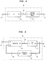
- the phase shift module 60 has a phase-locked loop 80 feeding a variable clock-shift module 82 through line 84.
- the phase-locked loop 80 shown in greater detail in Figure 3, has a comparator 90, a voltage-controlled oscillator 92, and a divide-by- n counter 94, interconnected by lines 96, 98, and 100 as shown in the figure.
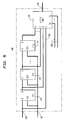
- the variable clock-shift module 82 is shown in Figure 4.
- the input (line 84) to the module 82 is connected to a divide-by- a counter 110 having b outputs, Q 1 through Q b , where b ⁇ ⁇ log2 a ⁇ in a binary system.
- These b outputs are connected by lines 112 to corresponding inputs 1 through b of a b -to- c decoder 114.
- the outputs 1 through c of the decoder 114 are connected in turn by lines 116 to inputs 1 through 2 d of a 2 d -to-1 multiplexer 118, respectively.
- the multiplexer 118 is enabled by select lines 122 connected to select inputs S1 through S d , and its output is connected to the D input of a D-type flip-flop 124.
- the clock signal is provided on a clock input line 126 tied to line 84.
- the output 64 of the module 82 is the Q output of the flip-flop 124.
- An example of the selectable outputs MUX1-MUX8 of the multiplexer 118 is illustrated by the timing diagram in Figure 6, which assumes a division-by-8 of the clock signal on line 84.
- bit-shifting module 140 An additional module, not shown in the overall block diagrams of Figures 1 and 2, is the bit-shifting module 140.
- This component can be inserted at the transmit port 44 of the transmitter-receiver 42 in the remote unit 40. However, one could place this module 140 on either side of the port 44.
- the purpose of the bit-shifting module 140 is to adjust the time of transmission of the data in some selected number of whole-bit increments, as determined by the user.
- the bit-shifting module 140 is a series of p cascaded D-type flip-flops 142, having a data input 148 connected to the D input of the first flip-flop FF1 142. The Q output of every flip-flop 142 but the last is tied to the D input of the next device.
- the clock input is derived from the output of the phase shift module 60 on line 68.
- the multiplexer 144 is enabled by z select lines 146 connected to select inputs S1 through S z , to provide an output 150.
- the local unit 10 transmits data along line 74 to the remote unit along with a synchronizing clock signal on line 76.
- a synchronizing clock signal on line 76.
- the data arrives at the transmitter-receiver 42 in the remote unit 40, it is clocked in by the received clock signal applied to receive clock port 50.
- T C propagation delay time of the cable
- D E propagation delay of the electronics of the remote unit 40
- T S time interval
- T S represents the shift in time of the data that must occur in the remote unit 40 so that the data is received at the local unit in an elapsed time of T D .
- the time shift T S would have possibly one, two, or more components.
- the first component is T Sf , the fractional bit time shift.
- T Sf the fractional bit time shift.
- T Sf + T Sb T D - (2 ⁇ T C ' + D E ) (4)
- T Sf and T Sb T D - (2 ⁇ T C ' + D E ) (4)
- the exact values of T Sf and T Sb are set by enabling the select lines 122 and 146 of the 2 d -to- 1 multiplexer 118 and the q -to- 1 multiplexer 144, respectively.
- the appropriate select lines 122 and 146 would be connected to ground or V CC , as required.
- T Sb independently of T Sf if whole-bit manipulation would provide sufficient resolution.
- MUX1 in Figure 6 an unshifted multiplexer output signal
- MUX1 in Figure 6 the signal on the input clock line 66. The latter could be provided directly to the transmit clock input 48, bypassing the phase shift module 60.
- the local and remote clocks may differ in frequency and duty cycle as required by the particular implementation.
- the transmit data rates and the synchronization clock frequency may differ.
- this scheme can be used with systems having more than two components. For example, where there are three or more communications modules connected in a system, the same method of adjusting the transmit time relative to a clock at the ultimate destination will serve to insure that data arrives at the receiving module at the proper time.
Landscapes
- Engineering & Computer Science (AREA)
- Computer Networks & Wireless Communication (AREA)
- Signal Processing (AREA)
- Synchronisation In Digital Transmission Systems (AREA)
Applications Claiming Priority (2)
| Application Number | Priority Date | Filing Date | Title |
|---|---|---|---|
| US99439292A | 1992-12-21 | 1992-12-21 | |
| US994392 | 1992-12-21 |
Publications (2)
| Publication Number | Publication Date |
|---|---|
| EP0603600A2 true EP0603600A2 (fr) | 1994-06-29 |
| EP0603600A3 EP0603600A3 (fr) | 1997-02-12 |
Family
ID=25540624
Family Applications (1)
| Application Number | Title | Priority Date | Filing Date |
|---|---|---|---|
| EP93119383A Ceased EP0603600A3 (fr) | 1992-12-21 | 1993-12-01 | Compensation du retard de trajet dans un système en bande ouverte. |
Country Status (2)
| Country | Link |
|---|---|
| US (1) | US5701334A (fr) |
| EP (1) | EP0603600A3 (fr) |
Cited By (3)
| Publication number | Priority date | Publication date | Assignee | Title |
|---|---|---|---|---|
| WO1999062219A3 (fr) * | 1998-05-25 | 2000-01-13 | Ericsson Telefon Ab L M | Procede relatif a la compensation du retard d'horloge |
| GB2538246A (en) * | 2015-05-11 | 2016-11-16 | Cirrus Logic Int Semiconductor Ltd | Digital accessory interface calibration |
| GB2542970A (en) * | 2014-12-02 | 2017-04-05 | Cirrus Logic Int Semiconductor Ltd | Digital accessory interface calibration |
Family Cites Families (10)
| Publication number | Priority date | Publication date | Assignee | Title |
|---|---|---|---|---|
| US3562432A (en) * | 1966-11-16 | 1971-02-09 | Communications Satellite Corp | Synchronizer for time division multiple access satellite communication system |
| JPS577490B2 (fr) * | 1974-02-26 | 1982-02-10 | ||
| US4792963A (en) * | 1982-06-14 | 1988-12-20 | Communications Satellite Corporation | Satellite clock system |
| US4757521A (en) * | 1984-05-17 | 1988-07-12 | Tie/Communications, Inc. | Synchronization method and apparatus for a telephone switching system |
| US4805195A (en) * | 1984-06-08 | 1989-02-14 | Amdahl Corporation | Selectable timing delay circuit |
| JPS61145995A (ja) * | 1984-12-20 | 1986-07-03 | Toshiba Corp | 集線分配装置 |
| JPS63120538A (ja) * | 1986-11-08 | 1988-05-24 | Nec Corp | タイミング再生回路 |
| PH27468A (en) * | 1988-03-21 | 1993-07-23 | First Pacific Communications C | Communication system using distributed switching for time division multiplexing of voice and data |
| JP2512786B2 (ja) * | 1988-07-18 | 1996-07-03 | 富士通株式会社 | 位相整合回路 |
| JPH07110075B2 (ja) * | 1989-07-13 | 1995-11-22 | 日本電気株式会社 | コードレス電話方式 |
-
1993
- 1993-12-01 EP EP93119383A patent/EP0603600A3/fr not_active Ceased
-
1996
- 1996-10-25 US US08/736,873 patent/US5701334A/en not_active Expired - Lifetime
Cited By (8)
| Publication number | Priority date | Publication date | Assignee | Title |
|---|---|---|---|---|
| WO1999062219A3 (fr) * | 1998-05-25 | 2000-01-13 | Ericsson Telefon Ab L M | Procede relatif a la compensation du retard d'horloge |
| GB2542970A (en) * | 2014-12-02 | 2017-04-05 | Cirrus Logic Int Semiconductor Ltd | Digital accessory interface calibration |
| US9836274B2 (en) | 2014-12-02 | 2017-12-05 | Cirrus Logic, Inc. | Digital accessory interface calibration |
| GB2542970B (en) * | 2014-12-02 | 2018-08-08 | Cirrus Logic Int Semiconductor Ltd | Digital accessory interface calibration |
| US10642570B2 (en) | 2014-12-02 | 2020-05-05 | Cirrus Logic, Inc. | Digital accessory interface calibration |
| GB2538246A (en) * | 2015-05-11 | 2016-11-16 | Cirrus Logic Int Semiconductor Ltd | Digital accessory interface calibration |
| GB2538246B (en) * | 2015-05-11 | 2018-06-20 | Cirrus Logic Int Semiconductor Ltd | Digital accessory interface calibration |
| US10042796B2 (en) | 2015-05-11 | 2018-08-07 | Cirrus Logic, Inc. | Digital accessory interface calibration |
Also Published As
| Publication number | Publication date |
|---|---|
| US5701334A (en) | 1997-12-23 |
| EP0603600A3 (fr) | 1997-02-12 |
Similar Documents
| Publication | Publication Date | Title |
|---|---|---|
| US4119796A (en) | Automatic data synchronizer | |
| US5379299A (en) | High speed propagation delay compensation network | |
| US20040062279A1 (en) | Method of synchronising data | |
| GB2369940A (en) | A clock recovery circuit using PLL | |
| JPH0220184B2 (fr) | ||
| US4430745A (en) | Digital data transmission | |
| US5793824A (en) | Digital phase locked loop having adaptive bandwidth for pulse stuffing synchronized digital communication system | |
| US4592050A (en) | Apparatus and method for providing a transparent interface across a satellite communications link | |
| US20020191723A1 (en) | Parallel signal automatic phase adjusting circuit | |
| EP0658990A1 (fr) | Procédé et dispositif d'alignement de paquets d'information numérique | |
| US6493408B1 (en) | Low-jitter data transmission apparatus | |
| US5123100A (en) | Timing control method in a common bus system having delay and phase correcting circuits for transferring data in synchronization and time division slot among a plurality of transferring units | |
| EP0312260A2 (fr) | Circuit de démultiplexage à grande vitesse | |
| EP0603600A2 (fr) | Compensation du retard de trajet dans un système en bande ouverte | |
| US5724392A (en) | Automatic path delay compensation system | |
| US5726651A (en) | Device for serializing high flow of binary data | |
| US4933955A (en) | Timing generator | |
| AU601574B2 (en) | Jitter control in digital communications links | |
| US4887261A (en) | Method and arrangement for transmitting a digital signal with a low bit rate in a time section, provided for higher bit rates, of a time division multiplexed signal | |
| US5974103A (en) | Deterministic exchange of data between synchronised systems separated by a distance | |
| AU667602B2 (en) | Multiplexing arrangement | |
| KR970000066B1 (ko) | 대기시간 지터 감소용 회로를 가진 디멀티플렉서 | |
| US4910755A (en) | Regenerator/synchronizer method and apparatus for missing-clock timing messages | |
| EP1511327A1 (fr) | Méthode de transmission de signaux vidéo | |
| US20060133816A1 (en) | Apparatus for synchronizing clock using source synchronous clock in optical transmission system |
Legal Events
| Date | Code | Title | Description |
|---|---|---|---|
| PUAI | Public reference made under article 153(3) epc to a published international application that has entered the european phase |
Free format text: ORIGINAL CODE: 0009012 |
|
| AK | Designated contracting states |
Kind code of ref document: A2 Designated state(s): DE FR GB IT |
|
| RAP1 | Party data changed (applicant data changed or rights of an application transferred) |
Owner name: SIEMENS ROLM COMMUNICATIONS INC. (A DELAWARE CORP. |
|
| PUAL | Search report despatched |
Free format text: ORIGINAL CODE: 0009013 |
|
| AK | Designated contracting states |
Kind code of ref document: A3 Designated state(s): DE FR GB IT |
|
| RAP1 | Party data changed (applicant data changed or rights of an application transferred) |
Owner name: SIEMENS BUSINESS COMMUNICATION SYSTEMS INC. |
|
| 17P | Request for examination filed |
Effective date: 19970825 |
|
| 17Q | First examination report despatched |
Effective date: 19990514 |
|
| RAP1 | Party data changed (applicant data changed or rights of an application transferred) |
Owner name: SIEMENS INFORMATION AND COMMUNICATION NETWORKS, IN |
|
| STAA | Information on the status of an ep patent application or granted ep patent |
Free format text: STATUS: THE APPLICATION HAS BEEN REFUSED |
|
| 18R | Application refused |
Effective date: 20010219 |