EP0603632A2 - Procédé pour la commande pour un arrangement de processeurs - Google Patents
Procédé pour la commande pour un arrangement de processeurs Download PDFInfo
- Publication number
- EP0603632A2 EP0603632A2 EP93119693A EP93119693A EP0603632A2 EP 0603632 A2 EP0603632 A2 EP 0603632A2 EP 93119693 A EP93119693 A EP 93119693A EP 93119693 A EP93119693 A EP 93119693A EP 0603632 A2 EP0603632 A2 EP 0603632A2
- Authority
- EP
- European Patent Office
- Prior art keywords
- program
- segment
- register
- address
- stored
- Prior art date
- Legal status (The legal status is an assumption and is not a legal conclusion. Google has not performed a legal analysis and makes no representation as to the accuracy of the status listed.)
- Granted
Links
Images


Classifications
-
- G—PHYSICS
- G06—COMPUTING OR CALCULATING; COUNTING
- G06F—ELECTRIC DIGITAL DATA PROCESSING
- G06F8/00—Arrangements for software engineering
- G06F8/40—Transformation of program code
- G06F8/41—Compilation
- G06F8/44—Encoding
- G06F8/447—Target code generation
-
- G—PHYSICS
- G06—COMPUTING OR CALCULATING; COUNTING
- G06F—ELECTRIC DIGITAL DATA PROCESSING
- G06F8/00—Arrangements for software engineering
- G06F8/40—Transformation of program code
- G06F8/41—Compilation
- G06F8/44—Encoding
- G06F8/443—Optimisation
Definitions
- processor-internal registers are relevant for addressing memory cells of a memory.
- the physical address that is to say the binary address value represented on the address lines of a microprocessor by digital level value, is determined by these microprocessors by an additive combination of the binary values stored in these registers internal to the processor.
- registers generally have a bit width that corresponds to the data bus format of the microprocessor (e.g. 16 bits) and a larger bit width is required to determine the physical address (e.g. 20 bits), one of the registers, which is referred to as a segment register, in relation to the other register, which is referred to as a top-up register, in terms of its position value shifted by the positions required for reaching the bit width required for the physical address (for example 4 bits) in the direction of more significant positions.
- This type of physical address generation can be understood in such a way that the content of the segment register represents the starting address for a memory area - called a segment - (e.g. with 64K addresses) in the addressable address area and the content of the top-up register Represents the address of a memory cell in the relevant segment.
- a segment - e.g. with 64K addresses
- a readjustment of the segment register is understandably only necessary if a new physical address to be set is outside the segment selected by the current content of the segment register. For this reason, different commands are available to the microprocessor for both the data and the program code addressing, the latter being of interest with regard to the segment register setting, particularly in the case of program jumps, depending on whether the segment register should remain unchanged during the addressing or whether a new value must be saved.
- corresponding commands e.g. call, JMP, RET
- 'NAH' if the segment register is not to be changed
- 'REMOTE' are the commands if there is a change in the segment register during execution the jump instruction is to be carried out.
- the object of the present invention is to control the processor device in such a way that the program modules of a system program can be compiled with the setting 'NAH', although the program modules are stored in different segments.
- the program modules required to form a program system are taken from a program library and the programs in the form of mnemonic instructions are converted into machine code.
- the compiler lacks the information as to whether the two program modules, that is to say the output program module and the target program module, are stored in the same segment or not.
- the setting 'REMOTE' has certain disadvantages, such as a longer program code and a longer execution time for jump instructions.
- the 'REMOTE' setting means that the segment register is unnecessarily reloaded in most jump instructions between the program modules.
- program modules are assumed which are compiled with the 'NAH' setting, regardless of the fact that the memory area of a segment is not sufficient to store all program modules.
- the program modules assigned to a respective segment are put together during the binding process, the address difference to the target program module being entered in the machine code of jump instructions.
- the address difference in the machine code of the jump instruction concerned becomes an address representing the target program module which is not occupied by any of the program modules is entered.
- the machine code remains unchanged in the memory, i. H. stored in the intended segments of the memory.
- a changeover control sequence is inserted in the memory, which has a 'REMOTE' jump instruction which sets the segment register to the address of the segment in which the target program module is stored.
- the attachment register is set to an address at which an entry control sequence is inserted in the memory, which has a 'NAH' jump instruction to the target program module.
- the advantage of this type of control of a microprocessor is that despite the memory requirement of the program modules that spans segments, the setting 'NAH' can be made when compiling them. Although in addition to the program modules of a segment an entry and a changeover control sequence are required, the memory requirement can be estimated with an implementation of the control method of the microprocessor according to the invention with approximately 30% fewer memory cells than for program modules compiled with the setting 'REMOTE' will.
- the known microprocessors also have segment-oriented address formation when addressing data, but for which other registers, namely a data segment register and at least one data record register, are available.
- this assumes that not only the program memory requirement but also the data memory requirement of the system program to be compiled does not exceed the memory area of a segment. In principle, no changes are made to the data segment register in data access instructions in the system program.
- microprocessor according to the invention is used for a system program that consists of several program segments, for processing them is controlled, a segment is sufficient as a data storage area, the program modules of the individual program segments can be assigned a common data segment.
- one data segment is not sufficient for the entire system program, so that at least two data segments must be provided, whereby only one of the data segments can be assigned to the program modules of a respective program segment due to the 'NAH' setting of the compilation device.
- the data segment register is set to the address of the data segment assigned to the relevant program segment at the beginning of the program processing.
- the object of an advantageous further development of the control method according to the invention is to switch the data segment register when a program jump from an output program module of a first program segment to a target program module of a second program segment, provided that a different data segment is assigned to the target program module than the output program module.
- an auxiliary cellar storage area is set up in a reserved location in the data segments, the program transfer parameters last stored in the cellar storage segment being copied into the auxiliary cellar storage area of the data segment assigned to the target program module.
- the auxiliary cellar memory area becomes the cellar memory, since the address of the data segment containing the target program module is stored in the cellar memory segment register.
- target program modules may contain jump instructions to a further target program module that is not assigned to the same program segment and for which the program transfer parameters last stored in the previously valid cellar memory segment are then copied in the auxiliary cellar memory area of the data segment assigned to it before the Jump instruction to the further target program module is executed.
- a return from a target program module leads back to the boarding control sequence, from which the address values in the data and cellar segment registers are then set again that were set before execution of the instructions of the boarding control sequence started.
- control effort can be implemented particularly effectively in the boarding control sequence if only two data segments are provided.
- memory cells required for control can be stored in an overlap of the data segments, so that these memory cells can be addressed from both data segments without having to reset the data segment register in each case.
- program modules PM1, .., PMn and program modules PMm, PMo which are stored in a first program memory segment SEG1 or in a second program memory segment SEG2 of the addressable memory area ASP.
- the start address of the first program memory segment SEG1 is denoted by S1ADR and that of the second program memory segment SEG2 by S2ADR.
- a changeover control sequence U is stored at the lower limit of the first program memory segment SEG1 and an entry control sequence E is stored at the upper end of the second program memory segment SEG2.
- the invention is not limited to a distribution of the program modules to two segments, and in the exemplary embodiment, to avoid redundancy, only a program jump from an output program module of a first program memory segment SEG1 to a target program module of a second program memory segment SEG2 is described.
- the program memory segments are also abbreviated as program segments.
- program jumps into the first program memory segment SEG1 can also be present in the second or in a third program memory segment, the second or third program memory segment then also having a transfer control sequence U and the first program segment SEG1 also a boarding control sequence E.
- the program modules PM1, .., PMo have been compiled by a compiler, and during the binding process the program modules PM1, .., PMn were assigned to the first program memory segment SEG1 and the program modules PMm, PMo to the second program memory segment SEG2.
- the program module PMn has a program jump to the program module PMo, the jump instruction being directed to an address AD o representing the program module PMo in the transfer control sequence U during the binding process.
- FIG. 3 An assembly listing for a universal transfer control sequence U is given in FIG. 3. It is essential that a jump instruction to the second program memory segment SEG2 is present in the transfer control sequence U when it is executed the microprocessor PR sets the start address S2ADR of the second program memory segment SEG2 in the program segment register CS and the start address ON of the entry control sequence E of the second program memory segment SEG2 in the program top-up register IP. After addressing this newly set physical address, the microprocessor PR obtains its control instructions from the boarding control sequence E.
- FIG. 3 An assembly listing of a universal boarding control sequence E can be seen from FIG. 3. It is essential that the boarding control sequence E has a jump instruction to the actual target program module PMo, with which the program top-up register IP of the microprocessor PR is set to the start address ADo of the program module PMo. Since the processing of the output program module is usually to be continued again after a target program module has been processed, the jump instructions used are so-called "call" instructions, in the execution of which the respective return address is stored by the microprocessor PR in the basement memory area (also called "stack").
- the control of the microprocessor PR required for such a return is symbolically indicated in FIG.
- a program jump instruction in the form of a RET return instruction is stored in the last position of this PMo program module.
- the address EIN + x is loaded in the program top-up register IP of the microprocessor PR, which follows the instruction to jump into the program module PMo in the boarding control sequence E.
- the microprocessor PR obtains this address from its cellar memory (“stack”).
- a return instruction of the "RETFAR" type is stored, during the execution of which the program segment register CS and the program top-up register IP are reset.
- Both registers CS, IP take over values from the "stack", the start address S1ADR of the first program memory segment SEG1 being set in the program segment register CS and the address a + y in the program top-up register IP, which has the instruction that follows the jump instruction in the program module PMn .
- the microprocessor PR can thus continue processing the program module PMn again.
- FIG. 3 shows an assembly listing for the boarding and transfer control sequence E, U, respectively. Based on the comments made, the control instructions listed should be self-explanatory for the specialist.
- FIGS. 4, 5 and 6 relate to the control processes required in the changeover control sequence E when a data segment is changed.
- the system program only consists of a first and a second program segment SEG1, SEG2, and the program modules PM1, .. .PMn of the first program segment SEG1 is assigned a first data segment DSEG1 and the program modules ... PMm, PMo, ... of the second program segment SEG2 a second data segment DSEG2.
- care must be taken that the data segment assigned to the respective target program module is always addressed by the microprocessor PR when the program segment is changed.
- the processor device has a data segment register DS and a plurality of data top registers DI, BX.
- a basement storage segment register SS and two basement storage top registers BP, SP are provided for basement storage addressing (stack addressing), the basement storage top register SP being automatically set to the current value of the basement storage by the microprocessor PR during storage operations.
- the control processes required for switching the data segment are carried out in the boarding control sequence E before the segment-related jump to the target program module PMo is carried out.
- the boarding control sequences differ only in terms of their address references, so that it is sufficient to explain the method steps for a switchover of the data segment to go into one of the two boarding control sequences E.
- the content of the data segment register becomes first DS checked for agreement with the start address of the data segment DSEG2 containing the boarding control sequence E. In the event that there is a match, the procedure is as described in connection with FIGS. 1, 2 and 3.
- the start address of the second data segment DSEG2 is stored in the data segment register DS.
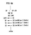
- the current address of an auxiliary cellar memory area HKS2 provided in the second data segment DSEG2 is read from a pointer memory cell ZSP2 stored in the overlap area UB of the two data segments DSEG1, DSEG2 and assigned to the second data segment DSEG2 and is stored in the data record register DI.
- the content of the basement storage segment register SS and the content of the basement storage essay register SP at the next address are stored in the address designated by the data segment register DS and the data top register DI - this is the first free memory cell in the auxiliary basement memory area HKS2.
- the content of the pointer memory cell ZSP1 assigned to the first data segment DSEG1 and also stored in the overlap area UB of the two data segments is then stored at the subsequent address in the auxiliary cellar storage area HKS2.
- a nesting index memory cell UMI which is also stored in the overlap area UB, is then read out and checked for its initial state, which in the present case is represented by the zero value.
- the nesting index memory cell UMI contains the zero value, which is equivalent to the fact that there is still no entry in the auxiliary cellar memory area in the first data segment DSEG1 HKS1 there, and the first entry is made in the auxiliary cellar storage area HKS2 of the second data segment DSEG2 at the present time.
- the zero value thus means that the minimum block nesting depth is present, that is to say that no intersegment program jumps have been carried out which have not led back to the starting program module.
- the address of the next free memory cell is assigned after the current address (SP -2) stored in the cellar memory segment - which is still set to the first data segment DSEG1 by the cellar memory segment register SS - in the pointer memory cell ZSP1 assigned to the first data segment DSEG1.
- the value in the nesting index memory cell UMI is then increased by one unit.
- the current address of the auxiliary cellar storage area HKS2 which is stored in the data add-on register DI, is transferred to the cellar storage add-on register SP and is stored in the cellar storage segment register SS the address of the second data segment DSEG2 is stored.
- the auxiliary cellar memory HKS2 becomes the cellar memory KSP for the target program module PMo, the address of which is subsequently stored in the program top-up register IP by means of a "call" jump instruction.
- the basement storage top register SP which currently points to the current address in the auxiliary basement storage area HKS2 of the second data segment DSEG2, is switched back by the number of program transfer parameters.
- the current address set in the basement storage register SP thus points to the content of the pointer storage cell ZSP1 stored in the third position in the auxiliary basement storage HKS2.
- This value stored at the current point in the auxiliary cellar memory HKS2 is transferred to the data record register DI and stored in the pointer memory cell ZSP1.
- the value stored second in the auxiliary cellar storage area HKS2 (content of the cellar storage register register SP) is then read out and transferred to the cellar storage register register SP.
- the value stored in the auxiliary cellar memory HKS2 (content of the cellar memory segment register SS) is copied into the cellar memory segment register SS and into the data segment register DS.
- FIG. 5 is intended to illustrate an assignment of the data segments DSEG1 and DSEG2 with respective auxiliary cellar storage areas HKS1, HKS2. Shown is an occupancy situation as it exists when a jump instruction to one of an output program module PMn assigned in the first program segment SEG1, to which the first data segment DSEG1 is assigned Target program module PMo was executed in the second program segment SEG2, to which the second data segment DSEG2 is assigned, and in this target program module PMo a jump instruction to a second target program module in the first program segment SEG1 and a jump instruction to a third target program module in the second program segment SEG2 was executed again that have not yet led to a return.
- an output program module PMn assigned in the first program segment SEG1
- Target program module PMo was executed in the second program segment SEG2, to which the second data segment DSEG2 is assigned
- FIG. 6 shows an assembly listing for the entry control sequence E in the second data segment DSEG2, which should be self-explanatory for the person skilled in the art.
- the boarding control sequence in the first program segment SEG1 differs only from the one explained in that the address of the second data segment DSEG2 is replaced by that of the first data segment DSEG1 , and the other pointer memory cell ZSP1 or ZSP2 is addressed.
Landscapes
- Engineering & Computer Science (AREA)
- General Engineering & Computer Science (AREA)
- Theoretical Computer Science (AREA)
- Software Systems (AREA)
- Physics & Mathematics (AREA)
- General Physics & Mathematics (AREA)
- Hardware Redundancy (AREA)
- Devices For Executing Special Programs (AREA)
- Executing Machine-Instructions (AREA)
- Exchange Systems With Centralized Control (AREA)
- Multi Processors (AREA)
Applications Claiming Priority (2)
| Application Number | Priority Date | Filing Date | Title |
|---|---|---|---|
| DE4243871 | 1992-12-23 | ||
| DE4243871 | 1992-12-23 |
Publications (3)
| Publication Number | Publication Date |
|---|---|
| EP0603632A2 true EP0603632A2 (fr) | 1994-06-29 |
| EP0603632A3 EP0603632A3 (fr) | 1995-01-04 |
| EP0603632B1 EP0603632B1 (fr) | 2000-09-13 |
Family
ID=6476417
Family Applications (1)
| Application Number | Title | Priority Date | Filing Date |
|---|---|---|---|
| EP93119693A Expired - Lifetime EP0603632B1 (fr) | 1992-12-23 | 1993-12-07 | Procédé pour la commande pour un arrangement de processeurs |
Country Status (4)
| Country | Link |
|---|---|
| EP (1) | EP0603632B1 (fr) |
| AT (1) | ATE196375T1 (fr) |
| DE (1) | DE59310101D1 (fr) |
| ES (1) | ES2150432T3 (fr) |
Families Citing this family (1)
| Publication number | Priority date | Publication date | Assignee | Title |
|---|---|---|---|---|
| CN115686627B (zh) * | 2022-09-07 | 2026-04-07 | 龙芯中科(合肥)技术有限公司 | 数据处理方法、装置、电子设备及介质 |
Family Cites Families (5)
| Publication number | Priority date | Publication date | Assignee | Title |
|---|---|---|---|---|
| DE2446245A1 (de) * | 1974-09-27 | 1976-04-01 | Siemens Ag | Verfahren zur verknuepfung und bereitstellung von programmen eines programmsystems fuer datenverarbeitungseinrichtungen, z.b. zentralsteuerwerk einer fernsprechvermittlungsanlage |
| JPS58142449A (ja) * | 1982-02-19 | 1983-08-24 | Hitachi Ltd | デ−タ処理装置 |
| JPH0283623A (ja) * | 1988-09-20 | 1990-03-23 | Nec Corp | マイクロプロセッサ |
| US5261101A (en) * | 1990-02-28 | 1993-11-09 | Microsoft Corporation | Method for calling and returning from subroutine that is invoked by either a near call or a far call |
| US5522072A (en) * | 1990-09-04 | 1996-05-28 | At&T Corp. | Arrangement for efficiently transferring program execution between subprograms |
-
1993
- 1993-12-07 EP EP93119693A patent/EP0603632B1/fr not_active Expired - Lifetime
- 1993-12-07 DE DE59310101T patent/DE59310101D1/de not_active Expired - Fee Related
- 1993-12-07 AT AT93119693T patent/ATE196375T1/de not_active IP Right Cessation
- 1993-12-07 ES ES93119693T patent/ES2150432T3/es not_active Expired - Lifetime
Also Published As
| Publication number | Publication date |
|---|---|
| EP0603632A3 (fr) | 1995-01-04 |
| ATE196375T1 (de) | 2000-09-15 |
| DE59310101D1 (de) | 2000-10-19 |
| EP0603632B1 (fr) | 2000-09-13 |
| ES2150432T3 (es) | 2000-12-01 |
Similar Documents
| Publication | Publication Date | Title |
|---|---|---|
| DE1901228C3 (de) | Datenverarbeitungsanlage mit Einrichtungen zur Wiederholung von Operationen bei Auftreten eines Fehlers | |
| AT398506B (de) | Signalverarbeitungsschaltung | |
| DE1956604A1 (de) | Datenverarbeitungsanlage mit einem Speichersystem | |
| DE2431379A1 (de) | Datenverarbeitungseinrichtung | |
| DE3126363A1 (de) | Verfahren und vorrichtung zur steuerung einer datenuebertragung mit direktem speicherzugriff | |
| DE1774908B2 (de) | Datenverarbeitungsanlage | |
| DE4220698A1 (de) | System zur dynamischen verknuepfung modularer abschnitte von computersoftware | |
| DE3031964A1 (de) | Rechnersystem, bei dem sich der programmspeicher zum durchlaufen eignet, wobei einem befehl nicht zugeordnete daten einzeln detektiert werden | |
| DE1180171B (de) | Zahlenrechner | |
| DE1900007A1 (de) | Datenverarbeitungssystem | |
| EP0603632B1 (fr) | Procédé pour la commande pour un arrangement de processeurs | |
| DE1774421B1 (de) | Mehrprogramm datenverarbeitungsanlage | |
| DE2015272A1 (de) | Programmleitwerk für eine digitale Datenverarbeitungsanlage | |
| EP0655688A2 (fr) | Extension de mémoire de programme pour microprocesseur | |
| DE1499286B2 (de) | Datenbearbeitungsanlage | |
| DE3009121C2 (de) | Mikroprogramm-Steuereinrichtung | |
| DE1499284A1 (de) | Datenbearbeitungsanlage | |
| DE69130400T2 (de) | Netzwerk und Verfahren zur Datenübertragung zwischen einem programmierbaren Steuergerät und mehreren Verarbeitungseinheiten | |
| DE1296427B (de) | Datenbearbeitungssystem | |
| DE2419522A1 (de) | Verfahren und anordnung zur unterteilung eines oder mehrerer nicht benutzter bereiche eines mit einem rechner verbundenen speichers | |
| DE68923044T2 (de) | Verfahren zur Datenübertragung zwischen Speichern. | |
| DE2204680A1 (de) | Mikroprogramm-steuereinrichtung | |
| EP0164578B1 (fr) | Procédé d'emmagasinage de données de communications groupées | |
| DE1449603A1 (de) | Analog-Digital- und Digital-Analog-Umsetzer-Verbindungssystem | |
| DE2544071C3 (de) | Mehrstufiges Arbeitsspeichersystem |
Legal Events
| Date | Code | Title | Description |
|---|---|---|---|
| PUAI | Public reference made under article 153(3) epc to a published international application that has entered the european phase |
Free format text: ORIGINAL CODE: 0009012 |
|
| AK | Designated contracting states |
Kind code of ref document: A2 Designated state(s): AT BE CH DE ES FR GB IT LI |
|
| PUAL | Search report despatched |
Free format text: ORIGINAL CODE: 0009013 |
|
| AK | Designated contracting states |
Kind code of ref document: A3 Designated state(s): AT BE CH DE ES FR GB IT LI |
|
| 17P | Request for examination filed |
Effective date: 19950607 |
|
| GRAG | Despatch of communication of intention to grant |
Free format text: ORIGINAL CODE: EPIDOS AGRA |
|
| GRAG | Despatch of communication of intention to grant |
Free format text: ORIGINAL CODE: EPIDOS AGRA |
|
| GRAH | Despatch of communication of intention to grant a patent |
Free format text: ORIGINAL CODE: EPIDOS IGRA |
|
| 17Q | First examination report despatched |
Effective date: 20000224 |
|
| GRAH | Despatch of communication of intention to grant a patent |
Free format text: ORIGINAL CODE: EPIDOS IGRA |
|
| GRAA | (expected) grant |
Free format text: ORIGINAL CODE: 0009210 |
|
| AK | Designated contracting states |
Kind code of ref document: B1 Designated state(s): AT BE CH DE ES FR GB IT LI |
|
| REF | Corresponds to: |
Ref document number: 196375 Country of ref document: AT Date of ref document: 20000915 Kind code of ref document: T |
|
| REG | Reference to a national code |
Ref country code: CH Ref legal event code: EP |
|
| REG | Reference to a national code |
Ref country code: CH Ref legal event code: NV Representative=s name: SIEMENS SCHWEIZ AG |
|
| REF | Corresponds to: |
Ref document number: 59310101 Country of ref document: DE Date of ref document: 20001019 |
|
| ITF | It: translation for a ep patent filed | ||
| REG | Reference to a national code |
Ref country code: ES Ref legal event code: FG2A Ref document number: 2150432 Country of ref document: ES Kind code of ref document: T3 |
|
| GBT | Gb: translation of ep patent filed (gb section 77(6)(a)/1977) |
Effective date: 20001116 |
|
| ET | Fr: translation filed | ||
| PLBE | No opposition filed within time limit |
Free format text: ORIGINAL CODE: 0009261 |
|
| STAA | Information on the status of an ep patent application or granted ep patent |
Free format text: STATUS: NO OPPOSITION FILED WITHIN TIME LIMIT |
|
| 26N | No opposition filed | ||
| PGFP | Annual fee paid to national office [announced via postgrant information from national office to epo] |
Ref country code: AT Payment date: 20011121 Year of fee payment: 9 |
|
| PGFP | Annual fee paid to national office [announced via postgrant information from national office to epo] |
Ref country code: ES Payment date: 20011213 Year of fee payment: 9 |
|
| PGFP | Annual fee paid to national office [announced via postgrant information from national office to epo] |
Ref country code: BE Payment date: 20011220 Year of fee payment: 9 |
|
| REG | Reference to a national code |
Ref country code: GB Ref legal event code: IF02 |
|
| PGFP | Annual fee paid to national office [announced via postgrant information from national office to epo] |
Ref country code: CH Payment date: 20020311 Year of fee payment: 9 |
|
| PG25 | Lapsed in a contracting state [announced via postgrant information from national office to epo] |
Ref country code: AT Free format text: LAPSE BECAUSE OF NON-PAYMENT OF DUE FEES Effective date: 20021207 |
|
| PG25 | Lapsed in a contracting state [announced via postgrant information from national office to epo] |
Ref country code: ES Free format text: LAPSE BECAUSE OF NON-PAYMENT OF DUE FEES Effective date: 20021209 |
|
| PG25 | Lapsed in a contracting state [announced via postgrant information from national office to epo] |
Ref country code: LI Free format text: LAPSE BECAUSE OF NON-PAYMENT OF DUE FEES Effective date: 20021231 Ref country code: CH Free format text: LAPSE BECAUSE OF NON-PAYMENT OF DUE FEES Effective date: 20021231 Ref country code: BE Free format text: LAPSE BECAUSE OF NON-PAYMENT OF DUE FEES Effective date: 20021231 |
|
| BERE | Be: lapsed |
Owner name: *SIEMENS A.G. Effective date: 20021231 |
|
| REG | Reference to a national code |
Ref country code: CH Ref legal event code: PL |
|
| PGFP | Annual fee paid to national office [announced via postgrant information from national office to epo] |
Ref country code: DE Payment date: 20040216 Year of fee payment: 11 |
|
| REG | Reference to a national code |
Ref country code: ES Ref legal event code: FD2A Effective date: 20021209 |
|
| PGFP | Annual fee paid to national office [announced via postgrant information from national office to epo] |
Ref country code: GB Payment date: 20041207 Year of fee payment: 12 |
|
| PGFP | Annual fee paid to national office [announced via postgrant information from national office to epo] |
Ref country code: FR Payment date: 20041223 Year of fee payment: 12 |
|
| PG25 | Lapsed in a contracting state [announced via postgrant information from national office to epo] |
Ref country code: DE Free format text: LAPSE BECAUSE OF NON-PAYMENT OF DUE FEES Effective date: 20050701 |
|
| PG25 | Lapsed in a contracting state [announced via postgrant information from national office to epo] |
Ref country code: IT Free format text: LAPSE BECAUSE OF NON-PAYMENT OF DUE FEES;WARNING: LAPSES OF ITALIAN PATENTS WITH EFFECTIVE DATE BEFORE 2007 MAY HAVE OCCURRED AT ANY TIME BEFORE 2007. THE CORRECT EFFECTIVE DATE MAY BE DIFFERENT FROM THE ONE RECORDED. Effective date: 20051207 Ref country code: GB Free format text: LAPSE BECAUSE OF NON-PAYMENT OF DUE FEES Effective date: 20051207 |
|
| GBPC | Gb: european patent ceased through non-payment of renewal fee |
Effective date: 20051207 |
|
| PG25 | Lapsed in a contracting state [announced via postgrant information from national office to epo] |
Ref country code: FR Free format text: LAPSE BECAUSE OF NON-PAYMENT OF DUE FEES Effective date: 20060831 |
|
| REG | Reference to a national code |
Ref country code: FR Ref legal event code: ST Effective date: 20060831 |