EP0603632B1 - Procédé pour la commande pour un arrangement de processeurs - Google Patents
Procédé pour la commande pour un arrangement de processeurs Download PDFInfo
- Publication number
- EP0603632B1 EP0603632B1 EP93119693A EP93119693A EP0603632B1 EP 0603632 B1 EP0603632 B1 EP 0603632B1 EP 93119693 A EP93119693 A EP 93119693A EP 93119693 A EP93119693 A EP 93119693A EP 0603632 B1 EP0603632 B1 EP 0603632B1
- Authority
- EP
- European Patent Office
- Prior art keywords
- program
- segment
- address
- stored
- register
- Prior art date
- Legal status (The legal status is an assumption and is not a legal conclusion. Google has not performed a legal analysis and makes no representation as to the accuracy of the status listed.)
- Expired - Lifetime
Links
Images


Classifications
-
- G—PHYSICS
- G06—COMPUTING OR CALCULATING; COUNTING
- G06F—ELECTRIC DIGITAL DATA PROCESSING
- G06F8/00—Arrangements for software engineering
- G06F8/40—Transformation of program code
- G06F8/41—Compilation
- G06F8/44—Encoding
- G06F8/447—Target code generation
-
- G—PHYSICS
- G06—COMPUTING OR CALCULATING; COUNTING
- G06F—ELECTRIC DIGITAL DATA PROCESSING
- G06F8/00—Arrangements for software engineering
- G06F8/40—Transformation of program code
- G06F8/41—Compilation
- G06F8/44—Encoding
- G06F8/443—Optimisation
Definitions
- processor devices e.g. B. microprocessors from the Siemens SAB8086 family are for addressing memory cells a memory each have at least two internal processor Register relevant. The physical address, so the on the address lines of a microprocessor by digital Binary address value represented by level value is used by these Microprocessors through an additive link of the in binary values stored in these processor-internal registers determined.
- the data bus format corresponding bit width of the microprocessor e.g. 16 bit
- one to determine the physical address larger bit width is required (e.g. 20 bit) is required for the additive linkage of one of the registers, the segment register to the other register, which is called the essay register, in its place to reach the for the physical address required bit width required digits (e.g. 4 bits) in Moved towards higher digits.
- This type of physical address generation can be used in the Be understood that the content of the segment register the start address for a memory area - segment called - (e.g. with 64K addresses) in the addressable address area represents and the content of the essay register the Represents the address of a memory cell in the relevant segment.
- - e.g. with 64K addresses
- the data contains, and an addressing one Memory cell containing program code no difference; however, are for data and program code addressing, respectively individual registers provided.
- a new setting of the segment register is understandable only required if there is a new one to be set physical address outside of the current one Contents of the segment register selected segment. Therefore stand for both data and program code addressing, the latter with regard to the segment register setting, especially for program jumps is of interest, different commands to the Microprocessor available depending on whether addressing the segment register should remain unchanged, or whether a new value has to be saved.
- the object of the present invention is the processor device to control so that the program modules of a system program can be compiled with the setting 'NAH', although the program modules are stored in different segments become.
- the 'FERN' setting means that most of the jump instructions between the program modules the segment register is unnecessarily reloaded.
- the program modules assigned to a respective segment are composed during the binding process, whereby in the machine code of jump instructions the address difference to Target program module is entered. With jump instructions, that cannot be "satisfied" because the target program module is not assigned to the segment in which the output program module is located in the machine code jump instruction concerned the address difference to a the address representing the target program module by none of the program modules is occupied.
- the attachment register is set to an address at which an entry control sequence is inserted in the memory which is a 'NAH' jump instruction to the target program module having.
- the known microprocessors also segment-oriented when addressing data Address formation, but for which other registers, namely a data segment register and at least one data record register be available.
- other registers namely a data segment register and at least one data record register be available.
- the compiler is assumed by this that not only the program memory requirement, but also the data memory requirement of the system program to be compiled in each case does not exceed the memory area of a segment. This is used for data access instructions in the system program principally no changes to the data segment register performed.
- the task of advantageous further training - claim 4 - of the control method according to the invention consists in in the event of a program jump from an output program module first program segment into a target program module second program segment a switchover of the data segment register if the target program module is different Data segment is assigned as the output program module.
- Jump instructions to another target program module may not be included in the same program segment is assigned and then for that in the auxiliary cellar storage area the most recently assigned data segment stored in the cellar storage segment valid until then Program transfer parameters are copied before the Jump instruction to the further target program module executed becomes.
- a return from a target program module leads back to the boarding control sequence, from which the address values in Data and basement storage segment registers reset before the execution of the instructions of the Boarding control sequence were set.
- the control effort in the Implement boarding control sequence if total only two data segments are provided. In this case, you can memory cells required for control in an overlap of the data segments are stored so that these Memory cells can be addressed from both data segments without having to reset the data segment register to have to.
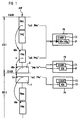
- FIG. 1 and 2 are program modules PM1, .., PMn and Program modules PMm, PMo symbolically represented in one first program memory segment SEG1 or in a second Program memory segment SEG2 of the addressable memory area ASP are saved.
- the start address of the first Program memory segment SEG1 is with S1ADR and that of second program memory segment SEG2 designated S2ADR.
- At the lower limit of the first program memory segment SEG1 is a transfer control sequence U and at the upper end of the second program memory segment SEG2 is an entry control sequence E saved.
- the invention is not based on a distribution of the program modules limited to two segments is, and in the embodiment to avoid Redundancy is just a program jump from an output program module a first program memory segment SEG1 in a target program module of a second program memory segment SEG2 is described.
- the program memory segments are abbreviated as program segments.
- the second or in a third Program memory segment also jumps to the first program Program memory segment SEG1 be present, in which case the second or third program memory segment also a transfer control sequence U and the first program segment SEG1 also have an entry control sequence E.
- the program modules PM1, .., PMo have been compiled by a compiler, and during the binding process the program modules PM1, .., PMn were assigned to the first program memory segment SEG1 and the program modules PMm, PMo to the second program memory segment SEG2.
- the program module PMn has a program jump to the program module PMo, the jump instruction being directed to an address AD o representing the program module PMo in the transfer control sequence U during the binding process.
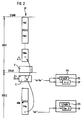
- PMo composing system program When executing the PM1 program module, .., PMo composing system program is in the microprocessor PR for program jump instructions within a program memory segment (e.g. from the PM1 program module) only the program register register IP changed, so z. B. on the start address ADn of a program module PMn set in the same program memory segment SEG1.
- a return instruction of the type "RETFAR” when executing them the program segment register CS and the program essay register IP can be reset.
- Both registers CS, IP take values from the "stack", being in the program segment register CS the start address S1ADR of the first program memory segment SEG1 and in the program register IP the Address a + y is set, which has the instruction which follows the jump instruction in the PMn program module.
- the microprocessor PR can process the program module PMn to be resumed.
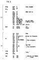
- FIG. 3 shows an assembly listing for the boarding and transfer control sequence E, U, respectively. Because of of the comments attached should be the control instructions listed be self-explanatory for the expert.
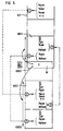
- Figures 4, 5 and 6 relate to those in the event of a data segment change necessary control processes in the transfer control sequence E.
- the system program only consists of a first and a second program segment SEG1, SEG2, and the Program modules PM1, ... PMn of the first program segment SEG1 a first data segment DSEG1 and the program modules ... PMm, PMo, ... of the second program segment SEG2 a second data segment DSEG2 is assigned.
- the program module of the other program segment is responsible for this to bear that with the change of the program segment too always the data segment assigned to the respective target program module is addressed by the microprocessor PR.
- the processor device has data memory addressing a data segment register DS and several data record registers DI, BX on.
- data segment register DS For cellar addressing (Stack addressing) are a basement memory segment register SS and two basement top registers BP, SP provided, the stack memory register SP from the microprocessor PR automatically for cellar storage operations is set to the current value of the cellar storage.
- the ones required for switching the data segment Control processes are in the boarding control sequence E before executing the segment-related jump to the target program module PMo executed.
- each of the program segments SEG1, SEG2 has its own boarding control sequence E, the boarding control sequences only differ regarding their address references, so that it is for explanation the procedural steps for switching the data segment is sufficient on one of the two boarding control sequences E go into more detail.
- the starting address of the second data segment DSEG2 in the data segment register DS saved. From one in the overlap area UB of the two Data segments DSEG1, DSEG2 deposited the second Pointer memory cell ZSP2 assigned to data segment DSEG2 becomes the current address of one in the second data segment Auxiliary cellar storage area HKS2 provided by DSEG2 read out and stored in the data record register DI. In the through the data segment register DS and the data record register DI designated address - this is the first free memory cell in the auxiliary cellar storage area HKS2 - the content of the cellar memory segment register SS and on the next address the content of the stack register register SP deposited. On the next one The address in the auxiliary cellar storage area HKS2 will then be the Contents of the and assigned to the first data segment DSEG1 also in the overlap area UB of the two data segments stored pointer memory cell ZSP1.
- the nesting index memory cell UMI contains the zero value, which is equivalent to the fact that in the first Data segment DSEG1 has no entry in the auxiliary cellar storage area HKS1 there, and in the auxiliary cellar storage area HKS2 of the second data segment DSEG2 at the present time the first entry is made.
- the zero value says so that the minimum block nesting depth is present, so no intersegment program jumps that were not returned to the initial program module to have.
- the nesting index memory cell UMI has a higher value, which is synonymous with that the target program module itself from a previous one Target program module is called, the target program modules different data segments are assigned, the Address of the next free memory cell after the current one Address (SP-2) in the basement segment - that through the basement segment register SS still on the first data segment DSEG1 is set - in the first data segment
- the pointer memory cell ZSP1 associated with DSEG1 is stored. Subsequently becomes the value in the nesting index memory cell UMI increased by one unit.
- the current address of the auxiliary cellar storage area HKS2 which are in the data record register DI is stored in the stack register register SP is transmitted and in the basement storage segment register SS the address of the second data segment DSEG2 is stored. This turns the HKS2 auxiliary cellar into a cellar KSP for the target program module PMo, whose address below by a "call" jump instruction into the program article register IP is saved.
- Figure 5 is intended to occupy the data segments DSEG1 and DSEG2 clarify with respective auxiliary cellar storage areas HKS1, HKS2.
- An occupancy situation like this is shown is present if one assigned to one in the first program segment SEG1 Output program module PMn, which the first data segment DSEG1 is assigned a jump instruction to one Target program module PMo in the second program segment SEG2, the the second data segment is assigned to DSEG2 and in this target program module PMo again one Jump instruction to a second target program module in the first Program segment SEG1 and from this a jump instruction to a third target program module in the second program segment SEG2 has not been run yet Have led back.
- FIG. 6 shows an assembly listing for the boarding control sequence E specified in the second data segment DSEG2, which for should be self-explanatory to the specialist.
Landscapes
- Engineering & Computer Science (AREA)
- General Engineering & Computer Science (AREA)
- Theoretical Computer Science (AREA)
- Software Systems (AREA)
- Physics & Mathematics (AREA)
- General Physics & Mathematics (AREA)
- Hardware Redundancy (AREA)
- Devices For Executing Special Programs (AREA)
- Executing Machine-Instructions (AREA)
- Exchange Systems With Centralized Control (AREA)
- Multi Processors (AREA)
Claims (8)
- Procédé pour la commande d'un arrangement de processeurs (PR) dans lequel, en vue de l'adressage d'un code programme, une génération d'adresse physique orientée segment est mise en oeuvre à l'aide d'un lien additif de valeurs d'adresse stockées dans un registre de segment de programme (CS) et dans au moins un registre de reprise de programme (IP), pour l'exécution d'un programme système composé d'une pluralité de modules de programme en utilisant un dispositif de compilation et d'édition de liens,dans lequel un premier nombre de modules de programme (PM1, . . ., PMn) est stocké dans un premier segment de programme (SEG1) et un second nombre de modules de programme (PMm, PMo) au moins dans un second segment de programme (SEG2) d'une mémoire adressable (ASP) par l'arrangement de processeurs,dans lequel, en raison d'un réglage 'PROCHE' lors de la compilation, les modules de programme ne présentent que des instructions de saut relatives au segment, à l'exécution desquelles le contenu du registre de segment de programme (CS) reste inchangé, etdans lequel, pour des sauts de programme de modules de programme (PM1, . . ., PMn) stockés dans le premier segment de programme (SEG1) à des modules de programme cible (. . ., PMo, . . .) stockés en dehors du premier segment de programme (SEG1), lors de l'exécution des instructions de saut concernées, une adresse cible (ADo) représentant l'adresse (ADo) du module de programme cible (Pmo) respectif dans le premier segment de programme (SEG1) est réglée dans le registre de reprise de programme (IP), à laquelle une séquence de commande de changement (U) est stockée dans la mémoire adressable (ASP),- - laquelle présente une instruction de saut 'LOIN', à l'exécution de laquelle est réglée dans le registre de segment de programme (CS), l'adresse (S2ADR) du segment de programme (SEG2) contenant le module de programme cible (PMo) et dans le registre de reprise de programme (IP), l'adresse (EIN) d'une séquence de commande d'entrée (E),--- laquelle présente une instruction de saut relative au segment, à l'exécution de laquelle l'adresse (ADo) du module de programme cible (PMo) est réglée dans le registre de reprise de programme (IP).
- Procédé selon la revendication 1, caractérisé en ce que, pour une exécution du programme système avec des modules de programme présentant des instructions de saut à d'autres modules de programme du programme système, à l'exécution desquelles à chaque fois une adresse de retour (a+y) est enregistrée dans une zone de pile (stack) de l'arrangement de processeurs (PR), et présentant en fin de module de programme à chaque fois une instruction de retour (RET) à l'exécution de laquelle l'adresse de retour (a+y) est extraite de la zone de pile et enregistrée dans le registre de reprise de programme (IP), la séquence de commande d'entrée (E) présente une instruction de retour 'loin' (RETFAR) à l'exécution de laquelle l'adresse de retour (a+y) est extraite de la zone de pile et enregistrée dans le registre de reprise de programme (IP) et une valeur d'adresse (S1ADR) déposée par la séquence de commande de changement (U) dans la zone de pile et désignant le premier segment de programme (SEG1) est extraite et enregistrée dans le registre de segment de programme (CS).
- Procédé selon la revendication 1 ou 2, caractérisé en ce que dans la séquence de commande de changement (U), une adresse cible représentative respective se voit attribuer un index individuel servant dans la séquence de commande d'entrée (E) de pointeur sur une table contenant des adresses de modules de programme cible.
- Procédé selon l'une des revendications 1 à 3, caractérisé
en ce que pour la commande d'un arrangement de processeurs (PR) dans lequel, en vue de l'adressage d'une mémoire de données et d'une mémoire pile, une génération d'adresse physique orientée segment est mise en oeuvre à l'aide d'un lien additif de valeurs d'adresse stockées dans un registre de segment de données (DS) resp. un registre de segment de pile (SS) et dans au moins un registre de reprise de données resp. un registre de reprise de pile (SP, BP), les modules de programme de chaque segment de programme (SEG1, SEG2) se voient attribuer un segment de données commun (DSEG1, DSEG2) pour le dépôt de données de programme essentiellement et un segment de pile commun pour le stockage intermédiaire de paramètres de commande et de transfert de modules de programme dans la mémoire adressable (ASP),
en ce que la séquence de commande d'entrée (E) présente, côté entrée, une interrogation à l'aide de laquelle est déterminé si la valeur d'adresse stockée dans le registre de segment de données (DS) correspond à l'adresse du segment de données (DSEG2) attribué au module de programme cible (PMo), en ce qu'en absence d'une correspondance, les étapes suivantes sont effectuées avant l'exécution de l'instruction de saut relative au segment :la valeur d'adresse du segment de données attribué au module de programme cible est enregistrée dans le registre de segment de données (DS), et, du segment de données (DSEG2) ainsi désigné, est extraite une cellule de mémoire de pointeur (ZSP2) servant à déposer l'adresse actuelle d'une zone de pile auxiliaire (HKS2) réservée dans le même segment de données (DSEG2),dans la zone de pile auxiliaire (HKS2) sont alors transférés d'abord au moins la valeur d'adresse stockée dans le registre de segment de pile (SS), la valeur d'adresse servant dans le registre de reprise de pile (SP) de pointeur sur l'adresse actuelle dans le segment de pile et le contenu de la cellule de mémoire de pointeur (ZSP1) stockée dans le segment de données (DSEG1) attribué au module de programme de sortie (PMn) respectif,puis un bloc de paramètres de paramètres de transfert de programme déposés dans le segment de pile à l'adresse actuelle est copié dans la zone de pile auxiliaire (HKS2),ensuite l'adresse actuelle de la pile auxiliaire (HKS2) dans le segment de données (DSEG2) est enregistrée dans le registre de reprise de pile (SP) et la valeur d'adresse du registre de segment de données (DS) dans le registre de segment de pile (SS). - Procédé selon la revendication 4, caractérisé en ce que respectivement une cellule de mémoire d'index d'emboítement (UMI) est prévue dans les segments de données (DSEG1, DSEG2), dans laquelle, en cas d'emboítements multiples, une valeur de niveau d'emboítement est déposée.
- Procédé selon la revendication 4 ou 5, avec deux segments de données (DSEG1, DSEG2) dont un premier est attribué aux modules de programme (PM1, . . ., PMn) du premier segment de programme (SEG1) et un second aux modules de programme (PMm, PMo) du second segment de programme (SEG2), caractérisé en ce que les deux segments de programme (DSEG1, DSEG2) présentent une zone de recouvrement (UB) dans laquelle sont placées les cellules de mémoire de pointeur (ZSP1, ZSP2) attribuées aux segments de données (DSEG1, DSEG2) et une cellule de mémoire d'index d'emboítement (UMI) commune,
en ce que dans la séquence de commande d'entrée (E), avant le transfert du bloc de paramètres et après l'enregistrement du contenu de la cellule de mémoire de pointeur (ZSP1) dans la zone de pile auxiliaire (HKS2), le contenu de la cellule de mémoire d'index d'emboítement (UMI) est vérifié quant à un écart par rapport à sa valeur de sortie, qui n'existe qu'en cas de niveau d'emboítement minimal des blocs, et qu'en présence d'un écart par rapport à la valeur de sortie, la valeur d'adresse stockée dans le registre de reprise de pile (SP) est enregistrée dans la cellule de mémoire de pointeur (ZSP1) du segment de données (DSEG1) attribué au module de programme de sortie (PMn) avant que le contenu de la cellule de mémoire d'index d'emboítement (UMI) ne soit commuté d'une unité. - Procédé selon l'une des revendications 2 à 6, caractérisé
en ce qu'après le retour relatif au segment du module de programme cible (PMo), la séquence de commande d'entrée (E) contient des instructions selon lesquelles l'adresse actuelle stockée dans le registre de reprise de pile (SP) est modifiée du nombre de paramètres de transfert de programme,
en ce que le contenu de la cellule de mémoire de pointeur (ZSP1) déposé avant le bloc de paramètres dans la zone de pile auxiliaire (HKS2) est enregistré dans la cellule de mémoire de pointeur (ZSP1) du segment de données (DSEG1) attribué au module de programme de sortie (PMn), et
en ce que les valeurs d'adresse déposées en première et seconde position dans la zone de pile auxiliaire (HKS2) sont enregistrées dans le registre de reprise de pile (SP) resp. dans le registre de segment de données et de pile (DS, SS) en fonction de leur signification au moment de l'enregistrement. - Dispositif commandé par programme, en particulier installation de postes téléphoniques supplémentaires dotée d'un agencement de processeurs commandé conformément au procédé selon l'une des revendications 1 à 7.
Applications Claiming Priority (2)
| Application Number | Priority Date | Filing Date | Title |
|---|---|---|---|
| DE4243871 | 1992-12-23 | ||
| DE4243871 | 1992-12-23 |
Publications (3)
| Publication Number | Publication Date |
|---|---|
| EP0603632A2 EP0603632A2 (fr) | 1994-06-29 |
| EP0603632A3 EP0603632A3 (fr) | 1995-01-04 |
| EP0603632B1 true EP0603632B1 (fr) | 2000-09-13 |
Family
ID=6476417
Family Applications (1)
| Application Number | Title | Priority Date | Filing Date |
|---|---|---|---|
| EP93119693A Expired - Lifetime EP0603632B1 (fr) | 1992-12-23 | 1993-12-07 | Procédé pour la commande pour un arrangement de processeurs |
Country Status (4)
| Country | Link |
|---|---|
| EP (1) | EP0603632B1 (fr) |
| AT (1) | ATE196375T1 (fr) |
| DE (1) | DE59310101D1 (fr) |
| ES (1) | ES2150432T3 (fr) |
Cited By (1)
| Publication number | Priority date | Publication date | Assignee | Title |
|---|---|---|---|---|
| CN115686627A (zh) * | 2022-09-07 | 2023-02-03 | 龙芯中科(合肥)技术有限公司 | 数据处理方法、装置、电子设备及介质 |
Family Cites Families (5)
| Publication number | Priority date | Publication date | Assignee | Title |
|---|---|---|---|---|
| DE2446245A1 (de) * | 1974-09-27 | 1976-04-01 | Siemens Ag | Verfahren zur verknuepfung und bereitstellung von programmen eines programmsystems fuer datenverarbeitungseinrichtungen, z.b. zentralsteuerwerk einer fernsprechvermittlungsanlage |
| JPS58142449A (ja) * | 1982-02-19 | 1983-08-24 | Hitachi Ltd | デ−タ処理装置 |
| JPH0283623A (ja) * | 1988-09-20 | 1990-03-23 | Nec Corp | マイクロプロセッサ |
| US5261101A (en) * | 1990-02-28 | 1993-11-09 | Microsoft Corporation | Method for calling and returning from subroutine that is invoked by either a near call or a far call |
| US5522072A (en) * | 1990-09-04 | 1996-05-28 | At&T Corp. | Arrangement for efficiently transferring program execution between subprograms |
-
1993
- 1993-12-07 EP EP93119693A patent/EP0603632B1/fr not_active Expired - Lifetime
- 1993-12-07 DE DE59310101T patent/DE59310101D1/de not_active Expired - Fee Related
- 1993-12-07 AT AT93119693T patent/ATE196375T1/de not_active IP Right Cessation
- 1993-12-07 ES ES93119693T patent/ES2150432T3/es not_active Expired - Lifetime
Cited By (1)
| Publication number | Priority date | Publication date | Assignee | Title |
|---|---|---|---|---|
| CN115686627A (zh) * | 2022-09-07 | 2023-02-03 | 龙芯中科(合肥)技术有限公司 | 数据处理方法、装置、电子设备及介质 |
Also Published As
| Publication number | Publication date |
|---|---|
| EP0603632A2 (fr) | 1994-06-29 |
| EP0603632A3 (fr) | 1995-01-04 |
| ATE196375T1 (de) | 2000-09-15 |
| DE59310101D1 (de) | 2000-10-19 |
| ES2150432T3 (es) | 2000-12-01 |
Similar Documents
| Publication | Publication Date | Title |
|---|---|---|
| DE1901228C3 (de) | Datenverarbeitungsanlage mit Einrichtungen zur Wiederholung von Operationen bei Auftreten eines Fehlers | |
| DE3416939A1 (de) | Verfahren zur steuerung von betriebseinrichtungen | |
| DE1956604A1 (de) | Datenverarbeitungsanlage mit einem Speichersystem | |
| DE1774908B2 (de) | Datenverarbeitungsanlage | |
| DE2331589A1 (de) | Datenverarbeitungsanordnung | |
| DE3126363A1 (de) | Verfahren und vorrichtung zur steuerung einer datenuebertragung mit direktem speicherzugriff | |
| DE10151091B4 (de) | Scheduling-System und Scheduling-Verfahren dafür | |
| DE2647574C2 (de) | Vorrichtung zum Verarbeiten von durch ein Anfangs- und Endzeichen begrenzten Datenfeldsegementen variabler Länge bei einem Umlaufspeicher | |
| DE2063195C2 (de) | Verfahren und Einrichtung zur Operationssteuerung einer Anzahl von externen Datenspeichern | |
| DE3938517C3 (de) | Verfahren zum Laden eines Steuerprogramms von einer externen Einrichtung in eine numerische Steuervorrichtung | |
| DE1900007A1 (de) | Datenverarbeitungssystem | |
| EP0603632B1 (fr) | Procédé pour la commande pour un arrangement de processeurs | |
| DE1285218B (de) | Datenverarbeitungsanlage | |
| DE1774421B1 (de) | Mehrprogramm datenverarbeitungsanlage | |
| DE1499286B2 (de) | Datenbearbeitungsanlage | |
| EP0655688A2 (fr) | Extension de mémoire de programme pour microprocesseur | |
| DE1499284A1 (de) | Datenbearbeitungsanlage | |
| DE1296427B (de) | Datenbearbeitungssystem | |
| DE1774849C3 (de) | Adressierungseinrichtung für eine Speicherabschnittkette | |
| DE69130400T2 (de) | Netzwerk und Verfahren zur Datenübertragung zwischen einem programmierbaren Steuergerät und mehreren Verarbeitungseinheiten | |
| DE2419522A1 (de) | Verfahren und anordnung zur unterteilung eines oder mehrerer nicht benutzter bereiche eines mit einem rechner verbundenen speichers | |
| DE68923044T2 (de) | Verfahren zur Datenübertragung zwischen Speichern. | |
| DE2110311A1 (de) | Statusmarkierung von Variablen | |
| DE2735874A1 (de) | Programmierbarer prozessrechner oder automat | |
| DE1449603A1 (de) | Analog-Digital- und Digital-Analog-Umsetzer-Verbindungssystem |
Legal Events
| Date | Code | Title | Description |
|---|---|---|---|
| PUAI | Public reference made under article 153(3) epc to a published international application that has entered the european phase |
Free format text: ORIGINAL CODE: 0009012 |
|
| AK | Designated contracting states |
Kind code of ref document: A2 Designated state(s): AT BE CH DE ES FR GB IT LI |
|
| PUAL | Search report despatched |
Free format text: ORIGINAL CODE: 0009013 |
|
| AK | Designated contracting states |
Kind code of ref document: A3 Designated state(s): AT BE CH DE ES FR GB IT LI |
|
| 17P | Request for examination filed |
Effective date: 19950607 |
|
| GRAG | Despatch of communication of intention to grant |
Free format text: ORIGINAL CODE: EPIDOS AGRA |
|
| GRAG | Despatch of communication of intention to grant |
Free format text: ORIGINAL CODE: EPIDOS AGRA |
|
| GRAH | Despatch of communication of intention to grant a patent |
Free format text: ORIGINAL CODE: EPIDOS IGRA |
|
| 17Q | First examination report despatched |
Effective date: 20000224 |
|
| GRAH | Despatch of communication of intention to grant a patent |
Free format text: ORIGINAL CODE: EPIDOS IGRA |
|
| GRAA | (expected) grant |
Free format text: ORIGINAL CODE: 0009210 |
|
| AK | Designated contracting states |
Kind code of ref document: B1 Designated state(s): AT BE CH DE ES FR GB IT LI |
|
| REF | Corresponds to: |
Ref document number: 196375 Country of ref document: AT Date of ref document: 20000915 Kind code of ref document: T |
|
| REG | Reference to a national code |
Ref country code: CH Ref legal event code: EP |
|
| REG | Reference to a national code |
Ref country code: CH Ref legal event code: NV Representative=s name: SIEMENS SCHWEIZ AG |
|
| REF | Corresponds to: |
Ref document number: 59310101 Country of ref document: DE Date of ref document: 20001019 |
|
| ITF | It: translation for a ep patent filed | ||
| REG | Reference to a national code |
Ref country code: ES Ref legal event code: FG2A Ref document number: 2150432 Country of ref document: ES Kind code of ref document: T3 |
|
| GBT | Gb: translation of ep patent filed (gb section 77(6)(a)/1977) |
Effective date: 20001116 |
|
| ET | Fr: translation filed | ||
| PLBE | No opposition filed within time limit |
Free format text: ORIGINAL CODE: 0009261 |
|
| STAA | Information on the status of an ep patent application or granted ep patent |
Free format text: STATUS: NO OPPOSITION FILED WITHIN TIME LIMIT |
|
| 26N | No opposition filed | ||
| PGFP | Annual fee paid to national office [announced via postgrant information from national office to epo] |
Ref country code: AT Payment date: 20011121 Year of fee payment: 9 |
|
| PGFP | Annual fee paid to national office [announced via postgrant information from national office to epo] |
Ref country code: ES Payment date: 20011213 Year of fee payment: 9 |
|
| PGFP | Annual fee paid to national office [announced via postgrant information from national office to epo] |
Ref country code: BE Payment date: 20011220 Year of fee payment: 9 |
|
| REG | Reference to a national code |
Ref country code: GB Ref legal event code: IF02 |
|
| PGFP | Annual fee paid to national office [announced via postgrant information from national office to epo] |
Ref country code: CH Payment date: 20020311 Year of fee payment: 9 |
|
| PG25 | Lapsed in a contracting state [announced via postgrant information from national office to epo] |
Ref country code: AT Free format text: LAPSE BECAUSE OF NON-PAYMENT OF DUE FEES Effective date: 20021207 |
|
| PG25 | Lapsed in a contracting state [announced via postgrant information from national office to epo] |
Ref country code: ES Free format text: LAPSE BECAUSE OF NON-PAYMENT OF DUE FEES Effective date: 20021209 |
|
| PG25 | Lapsed in a contracting state [announced via postgrant information from national office to epo] |
Ref country code: LI Free format text: LAPSE BECAUSE OF NON-PAYMENT OF DUE FEES Effective date: 20021231 Ref country code: CH Free format text: LAPSE BECAUSE OF NON-PAYMENT OF DUE FEES Effective date: 20021231 Ref country code: BE Free format text: LAPSE BECAUSE OF NON-PAYMENT OF DUE FEES Effective date: 20021231 |
|
| BERE | Be: lapsed |
Owner name: *SIEMENS A.G. Effective date: 20021231 |
|
| REG | Reference to a national code |
Ref country code: CH Ref legal event code: PL |
|
| PGFP | Annual fee paid to national office [announced via postgrant information from national office to epo] |
Ref country code: DE Payment date: 20040216 Year of fee payment: 11 |
|
| REG | Reference to a national code |
Ref country code: ES Ref legal event code: FD2A Effective date: 20021209 |
|
| PGFP | Annual fee paid to national office [announced via postgrant information from national office to epo] |
Ref country code: GB Payment date: 20041207 Year of fee payment: 12 |
|
| PGFP | Annual fee paid to national office [announced via postgrant information from national office to epo] |
Ref country code: FR Payment date: 20041223 Year of fee payment: 12 |
|
| PG25 | Lapsed in a contracting state [announced via postgrant information from national office to epo] |
Ref country code: DE Free format text: LAPSE BECAUSE OF NON-PAYMENT OF DUE FEES Effective date: 20050701 |
|
| PG25 | Lapsed in a contracting state [announced via postgrant information from national office to epo] |
Ref country code: IT Free format text: LAPSE BECAUSE OF NON-PAYMENT OF DUE FEES;WARNING: LAPSES OF ITALIAN PATENTS WITH EFFECTIVE DATE BEFORE 2007 MAY HAVE OCCURRED AT ANY TIME BEFORE 2007. THE CORRECT EFFECTIVE DATE MAY BE DIFFERENT FROM THE ONE RECORDED. Effective date: 20051207 Ref country code: GB Free format text: LAPSE BECAUSE OF NON-PAYMENT OF DUE FEES Effective date: 20051207 |
|
| GBPC | Gb: european patent ceased through non-payment of renewal fee |
Effective date: 20051207 |
|
| PG25 | Lapsed in a contracting state [announced via postgrant information from national office to epo] |
Ref country code: FR Free format text: LAPSE BECAUSE OF NON-PAYMENT OF DUE FEES Effective date: 20060831 |
|
| REG | Reference to a national code |
Ref country code: FR Ref legal event code: ST Effective date: 20060831 |