EP0603780A2 - Procédé de croissance d'un semi-conducteur composé sur une pastille de silicium - Google Patents
Procédé de croissance d'un semi-conducteur composé sur une pastille de silicium Download PDFInfo
- Publication number
- EP0603780A2 EP0603780A2 EP93120495A EP93120495A EP0603780A2 EP 0603780 A2 EP0603780 A2 EP 0603780A2 EP 93120495 A EP93120495 A EP 93120495A EP 93120495 A EP93120495 A EP 93120495A EP 0603780 A2 EP0603780 A2 EP 0603780A2
- Authority
- EP
- European Patent Office
- Prior art keywords
- compound semiconductor
- silicon wafer
- temperature
- grown
- layer
- Prior art date
- Legal status (The legal status is an assumption and is not a legal conclusion. Google has not performed a legal analysis and makes no representation as to the accuracy of the status listed.)
- Granted
Links
Images


Classifications
-
- H—ELECTRICITY
- H10—SEMICONDUCTOR DEVICES; ELECTRIC SOLID-STATE DEVICES NOT OTHERWISE PROVIDED FOR
- H10P—GENERIC PROCESSES OR APPARATUS FOR THE MANUFACTURE OR TREATMENT OF DEVICES COVERED BY CLASS H10
- H10P14/00—Formation of materials, e.g. in the shape of layers or pillars
- H10P14/20—Formation of materials, e.g. in the shape of layers or pillars of semiconductor materials
- H10P14/36—Formation of materials, e.g. in the shape of layers or pillars of semiconductor materials characterised by treatments done before the formation of the materials
- H10P14/3602—In-situ cleaning
-
- H—ELECTRICITY
- H10—SEMICONDUCTOR DEVICES; ELECTRIC SOLID-STATE DEVICES NOT OTHERWISE PROVIDED FOR
- H10P—GENERIC PROCESSES OR APPARATUS FOR THE MANUFACTURE OR TREATMENT OF DEVICES COVERED BY CLASS H10
- H10P14/00—Formation of materials, e.g. in the shape of layers or pillars
- H10P14/20—Formation of materials, e.g. in the shape of layers or pillars of semiconductor materials
- H10P14/24—Formation of materials, e.g. in the shape of layers or pillars of semiconductor materials using chemical vapour deposition [CVD]
-
- H—ELECTRICITY
- H10—SEMICONDUCTOR DEVICES; ELECTRIC SOLID-STATE DEVICES NOT OTHERWISE PROVIDED FOR
- H10P—GENERIC PROCESSES OR APPARATUS FOR THE MANUFACTURE OR TREATMENT OF DEVICES COVERED BY CLASS H10
- H10P14/00—Formation of materials, e.g. in the shape of layers or pillars
- H10P14/20—Formation of materials, e.g. in the shape of layers or pillars of semiconductor materials
- H10P14/29—Formation of materials, e.g. in the shape of layers or pillars of semiconductor materials characterised by the substrates
- H10P14/2901—Materials
- H10P14/2902—Materials being Group IVA materials
- H10P14/2905—Silicon, silicon germanium or germanium
-
- H—ELECTRICITY
- H10—SEMICONDUCTOR DEVICES; ELECTRIC SOLID-STATE DEVICES NOT OTHERWISE PROVIDED FOR
- H10P—GENERIC PROCESSES OR APPARATUS FOR THE MANUFACTURE OR TREATMENT OF DEVICES COVERED BY CLASS H10
- H10P14/00—Formation of materials, e.g. in the shape of layers or pillars
- H10P14/20—Formation of materials, e.g. in the shape of layers or pillars of semiconductor materials
- H10P14/29—Formation of materials, e.g. in the shape of layers or pillars of semiconductor materials characterised by the substrates
- H10P14/2926—Crystal orientations
-
- H—ELECTRICITY
- H10—SEMICONDUCTOR DEVICES; ELECTRIC SOLID-STATE DEVICES NOT OTHERWISE PROVIDED FOR
- H10P—GENERIC PROCESSES OR APPARATUS FOR THE MANUFACTURE OR TREATMENT OF DEVICES COVERED BY CLASS H10
- H10P14/00—Formation of materials, e.g. in the shape of layers or pillars
- H10P14/20—Formation of materials, e.g. in the shape of layers or pillars of semiconductor materials
- H10P14/32—Formation of materials, e.g. in the shape of layers or pillars of semiconductor materials characterised by intermediate layers between substrates and deposited layers
- H10P14/3202—Materials thereof
- H10P14/3214—Materials thereof being Group IIIA-VA semiconductors
- H10P14/3221—Arsenides
-
- H—ELECTRICITY
- H10—SEMICONDUCTOR DEVICES; ELECTRIC SOLID-STATE DEVICES NOT OTHERWISE PROVIDED FOR
- H10P—GENERIC PROCESSES OR APPARATUS FOR THE MANUFACTURE OR TREATMENT OF DEVICES COVERED BY CLASS H10
- H10P14/00—Formation of materials, e.g. in the shape of layers or pillars
- H10P14/20—Formation of materials, e.g. in the shape of layers or pillars of semiconductor materials
- H10P14/32—Formation of materials, e.g. in the shape of layers or pillars of semiconductor materials characterised by intermediate layers between substrates and deposited layers
- H10P14/3242—Structure
- H10P14/3244—Layer structure
- H10P14/3254—Graded layers
-
- H—ELECTRICITY
- H10—SEMICONDUCTOR DEVICES; ELECTRIC SOLID-STATE DEVICES NOT OTHERWISE PROVIDED FOR
- H10P—GENERIC PROCESSES OR APPARATUS FOR THE MANUFACTURE OR TREATMENT OF DEVICES COVERED BY CLASS H10
- H10P14/00—Formation of materials, e.g. in the shape of layers or pillars
- H10P14/20—Formation of materials, e.g. in the shape of layers or pillars of semiconductor materials
- H10P14/32—Formation of materials, e.g. in the shape of layers or pillars of semiconductor materials characterised by intermediate layers between substrates and deposited layers
- H10P14/3242—Structure
- H10P14/3256—Microstructure
-
- H—ELECTRICITY
- H10—SEMICONDUCTOR DEVICES; ELECTRIC SOLID-STATE DEVICES NOT OTHERWISE PROVIDED FOR
- H10P—GENERIC PROCESSES OR APPARATUS FOR THE MANUFACTURE OR TREATMENT OF DEVICES COVERED BY CLASS H10
- H10P14/00—Formation of materials, e.g. in the shape of layers or pillars
- H10P14/20—Formation of materials, e.g. in the shape of layers or pillars of semiconductor materials
- H10P14/34—Deposited materials, e.g. layers
- H10P14/3402—Deposited materials, e.g. layers characterised by the chemical composition
- H10P14/3414—Deposited materials, e.g. layers characterised by the chemical composition being group IIIA-VIA materials
- H10P14/3421—Arsenides
-
- Y—GENERAL TAGGING OF NEW TECHNOLOGICAL DEVELOPMENTS; GENERAL TAGGING OF CROSS-SECTIONAL TECHNOLOGIES SPANNING OVER SEVERAL SECTIONS OF THE IPC; TECHNICAL SUBJECTS COVERED BY FORMER USPC CROSS-REFERENCE ART COLLECTIONS [XRACs] AND DIGESTS
- Y10—TECHNICAL SUBJECTS COVERED BY FORMER USPC
- Y10S—TECHNICAL SUBJECTS COVERED BY FORMER USPC CROSS-REFERENCE ART COLLECTIONS [XRACs] AND DIGESTS
- Y10S438/00—Semiconductor device manufacturing: process
- Y10S438/933—Germanium or silicon or Ge-Si on III-V
Definitions
- the present invention relates to a method of epitaxially growing a compound semiconductor or a silicon wafer.
- a defect called an anti-phase domain because different atoms are arranged on the same plane and a number of crystal defects called dislocation caused by a difference between lattice constants and thermal expansion factors inherent to heteroepitaxy.
- a method called a two-step growth method is generally used in growing a compound semiconductor, which is disclosed in JP-A-61-26216 and JP-A-61-70715.
- Fig. 7 illustrates a supply of source materials and a temperature change of a susceptor according to the two-step growth method. For the comparison with Fig.
- a supply of source materials and a temperature change of a susceptor according to homoepitaxy used for forming a compound semiconductor is shown in Fig. 6.
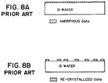
- a conventional two-step growth method will be described with reference to Figs. 7, 8A, and 8B.
- a silicon wafer is cleaned which has the surface inclined by 2 to 5 degrees in the direction ⁇ 1 1 0> from the plane (0 0 1).
- the surface oxide film of the wafer is first exposed to hydrofluoric acid to etch it, and then subjected to a thermal treatment under a hydrogen atmosphere at a temperature of 800 °C or higher within a compound semiconductor manufacturing apparatus to completely remove the surface oxide film (Step (1)).
- Step (2) source material gases are introduced into the apparatus to deposit amorphous compound semiconductor to a thickness of 20 to 200 nm.
- Step (3) the temperature is raised to about 650 to 700 °C.
- the amorphous compound semiconductor changes to a single crystal layer.
- the single crystal layer as a buffer layer, a compound semiconductor is grown on it (Step (4)).
- a thin amorphous layer is first formed (Fig. 8A) which is re-crystallized during the temperature raising period to form a buffer layer of poor surface flatness (Fig. 8B). Since a growth layer is formed on such a buffer layer, from the viewpoint of surface morphology, the growth layer has a waved surface characteristic of GaAs/Si without reflecting the flatness of the silicon wafer. This uneven surface adversely affects the distribution of threshold values of LSIs. A report regarding this problem was presented at the Spring Meeting of the Japan Society of Applied Physics, 1992. This report teaches that the surface flatness can be improved if the growth is temporarily terminated under the uneven surface condition, and it is resumed after the surface is polished to the degree of the same flatness as the silicon wafer.
- the first problem associated with the above-described conventional technique is that the productivity is very low as compared to the homoepitaxy illustrated in Fig. 6, because the second-step growth method requires the four steps, including a step of cleaning the surface of a wafer, a step of setting a temperature suitable for the deposition of an amorphous layer, a step of raising the temperature suitable for crystallizing the amorphous layer into a buffer layer, and a step of setting the temperature suitable for growing a compound semiconductor.
- the second problem resides in the verification that because the amorphous layer is as thin as 200 nm or less, the single crystal layer crystallized during the temperature raising period is not two-dimensionally continuous but is formed by many islands and does not cover the whole surface of the silicon wafer (The Sumitomo Search No. 47, October 1991, Applied Physic Letter 59 (26), 23 December 1991).
- the surface of an epitaxial film grown by the two-step growth method is rough.
- the root mean square roughness is 4 to 5 nm even in an excellent case according to the evaluation by AFM (Atomic Force Microscopy).
- This conventional technique can be regarded as still not being practical when considering a roughness of 3 nm as a minimum required for an LSI level.
- the regrowth method after polishing which attains an improved surface flatness of an LSI level, has been tried (GaAs Related Compounds, 1991, Karuizawa, Inst. Phys. Ser. No. 129, Chapter 3, p. 175), the number of necessary manufacturing steps increases considerably, the productivity lowers, and the manufacturing costs become high. It has been long desired therefore to provide an as-grown wafer to have a surface flatness of about 3 nm comparable with an LSI level.
- a buffer layer of a compound semiconductor as thin as 200 nm or less changes, during the temperature raising period (Step 2) shown in Fig. 7, from a thin amorphous continuous film shown in Fig. 8A to a re-crystallized as a single crystal compound semiconductor of single domain islands shown in Fig. 8B.
- the density of this single crystal buffer layer is more coarse than an ordinary single crystal.
- a compound semiconductor grown on the buffer layer reflects the inferior flatness of the layer, and other layers grown on the compound semiconductor layer also reflect it.
- the buffer layer is made thicker in order to replenish source materials, rearrangement of crystals is hindered much, forming a whity single crystal layer with an anti-phase domain instead of a layer with a single domain. From the above reasons, the conventional growth technique is not suitable for growing compound semiconductors an a silicon wafer having a surface flatness comparable with LSI level electronic devices.
- a method of epitaxially growing compound semiconductors on a silicon wafer in which an amorphous buffer layer is grown on a clean silicon wafer not at a constant temperature as in the case of the conventional technique, but during a temperature raising period, from a temperature allowing source materials necessary for the growth of the compound semiconductor to be dissolved, to a temperature allowing the growth of single crystal of the compound semiconductor. Accordingly, the buffer layer having an excellent coverage of the silicon wafer which leads to an improved surface flatness can be obtained, and very simplified processes can be realized.
- a gallium arsenide layer is grown by a vapor deposition method particularly by MOCVD, by using a Si wafer. Calibration of the growth temperature was carried out by measuring the melting point of aluminum particles placed on a wafer.
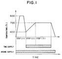
- Fig. 1 is a graph illustrating a temperature change of a susceptor and a supply of source materials according to the first embodiment of a method of manufacturing a compound semiconductor of the present invention.
- the term "temperature” is intended to mean the temperature of a susceptor.
- a silicon wafer having the surface tilted by 3 degrees in the direction ⁇ 1 1 0> from the plane (0 0 1) is subjected to a surface cleaning process for 5 minutes at a temperature of 800 °C or higher under a hydrogen carrier gas.
- one of the source materials trimethylgallium (TMG)
- TMG trimethylgallium
- the temperature is thereafter raised to 600 to 750 ° in 4 to 8 minutes.
- the temperature range from 600 to 750 °C is suitable for a single crystal growth temperature.
- a buffer layer is formed to a thickness from 100 nm or more to 250 nm or less (the buffer layer formed during this temperature raising period is called hereinafter a temperature raising growth layer).
- the source material is continuously supplied (Step (3)) until a desired film thickness is obtained when the supply of the source material is stopped.
- Another source material, arsine is preferably supplied at all Steps in order to prevent attachment of impurities from the susceptor, and re-vaporization of As.
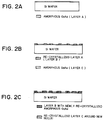
- Step (2) provides both the growth of the amorphous buffer layer mainly at the lower temperature and the re-crystallization of the amorphous material during the temperature raising period. Accordingly, not only a single crystal of compound semiconductor with a single domain can be grown, but also a silicon wafer fully covered with the temperature raising growth layer can be obtained. Because the source material is continuously supplied in the temperature range within which both the re-crystallization of already deposited amorphous material (layer B shown in Fig. 2B) and the growth of new amorphous material (layer C in Fig. 2B) are carried out, the surface of the silicon wafer not completely covered with the single crystal layer shown in Fig. 8B is covered with the newly supplied source material (layer C) as shown in Fig. 2B.
- a single crystal growth layer formed on the temperature raising growth layer has an excellent surface as small as a root mean square roughness of 3 nm or less measured by AFM, which allows electronic devices at an LSI level to be manufactured.
- an independent process of growing a buffer layer at the low temperature is not needed.
- an as-grown wafer has a surface morphology comparable with an LSI level.
- the conventional re-growth after polishing is not necessary.
- With a very simple growth method it is possible to provide a silicon wafer with a compound semiconductor epitaxial layer having an excellent surface flatness suitable for manufacturing LSIs.
- a GaAs/Si heteroepitaxial wafer having an excellent surface flatness (3 nm of a root mean square roughness measured by AFM) can be manufactured easily by the embodiment growth method having a smaller number of processes than a conventional method.
- the crystal property of the epitaxial growth layer having a thickness of 3 ⁇ m was evaluated as having a half-value width of 200 seconds measured by X ray.
- the half-value width of a growth film formed by a conventional two-step growth method is 230 seconds. It was verified accordingly that also the crystal property was improved by the embodiment growth method.
- a silicon wafer having the surface tilted by three degrees in the direction ⁇ 1 1 0> from the plane (0 0 1) is annealed at a temperature of 1100 °C under a hydrogen atmosphere in an apparatus other than an MOCVD growth apparatus, and etched by hydrofluoric acid. Thereafter, the silicon wafer is placed on a susceptor of the MOCVD apparatus, taking care of the silicon wafer so as not to be contaminated.
- a compound semiconductor is grown under the condition of a temperature change and a source material supply illustrated in Fig. 3. Specifically, at Step (2) where the temperature is continuously raised, one of the source materials, TMG, is supplied starting from a temperature of 400 °C.
- the other material, arsine, is preferably supplied at all Steps from the same reason described with the first embodiment.
- a GaAs/Si heteroepitaxial wafer having a desired excellent surface flatness was obtained with the number of processes less than a conventional method.
- the crystal property of the heteroepitaxial layer formed by the second embodiment was improved to the same extent as the first embodiment.
- the different points from the first embodiment reside in that at the temperature raising Step (2) from 400 °C to 700 °C, TMG is supplied for about one minute at the temperature range from 400 to 520 °C to form the temperature raising layer to a thickness of 40 nm, and thereafter, the supply of TMG is stopped. It is preferable to supply arsine continuously from the same reason described with the first embodiment.
- TMG is again supplied to continue the crystal growth.
- the other points are the same as in the first embodiment.
- a GaAs/Si heteroepitaxial wafer having a desired excellent surface flatness was obtained with the number of processes (steps) being less than in a conventional method.
- the crystal performance of the heteroepitaxial layer formed by the second embodiment was improved to the same extent as the first embodiment (2 to 3 nm of the root mean square roughness measured by AFM).
- the different points from the first embodiment reside in that at the temperature raising Step (2) from 400 °C to 700 °C, TMG is not supplied in the temperature range from 520 to 560 °C. It is preferable to supply arsine continuously for the same reason described with the first embodiment. The other points are the same as the first embodiment. In this manner, a GaAs/Si heteroepitaxial wafer having the desired excellent surface flatness was obtained with the number of processes (steps) being less than in a conventional method. The crystal performance of the heteroepitaxial layer formed by the second embodiment was improved to the same extent as the first embodiment (2 to 3 nm of the root mean square roughness measured by AFM).
- both the complicated growth processes and the poor surface morphology which have been the problem associated with the conventional two-stage growth method as a technique of heteroepitaxially growing a compound semiconductor on a silicon wafer, can be improved, with an improved productivity of GaAs/Si wafers and an improved wafer flatness necessary for IC processes.
- the crystal property as evaluated from a half-value width of an X-ray can be improved by about 10%, allowing applications not only for electronic devices such as ICs, but also for optoelectronic devices requiring good crystal properties.
Applications Claiming Priority (4)
| Application Number | Priority Date | Filing Date | Title |
|---|---|---|---|
| JP35720892 | 1992-12-21 | ||
| JP35720992A JPH06188164A (ja) | 1992-12-21 | 1992-12-21 | エピタキシャル成長用基板及びエピタキシャル成長方法 |
| JP357208/92 | 1992-12-21 | ||
| JP357209/92 | 1992-12-21 |
Publications (3)
| Publication Number | Publication Date |
|---|---|
| EP0603780A2 true EP0603780A2 (fr) | 1994-06-29 |
| EP0603780A3 EP0603780A3 (fr) | 1995-03-22 |
| EP0603780B1 EP0603780B1 (fr) | 1998-04-29 |
Family
ID=26580570
Family Applications (1)
| Application Number | Title | Priority Date | Filing Date |
|---|---|---|---|
| EP93120495A Expired - Lifetime EP0603780B1 (fr) | 1992-12-21 | 1993-12-19 | Procédé de croissance d'un semi-conducteur composé sur une pastille de silicium |
Country Status (3)
| Country | Link |
|---|---|
| US (1) | US5438951A (fr) |
| EP (1) | EP0603780B1 (fr) |
| DE (1) | DE69318271T2 (fr) |
Cited By (1)
| Publication number | Priority date | Publication date | Assignee | Title |
|---|---|---|---|---|
| GB2351841A (en) * | 1999-07-06 | 2001-01-10 | Sharp Kk | A semiconductor laser device |
Families Citing this family (5)
| Publication number | Priority date | Publication date | Assignee | Title |
|---|---|---|---|---|
| WO1999019546A1 (fr) | 1997-10-10 | 1999-04-22 | Cornell Research Foundation, Inc. | Procedes de croissance de couches heteroepitaxiales sans defaut |
| US6274463B1 (en) | 2000-07-31 | 2001-08-14 | Hewlett-Packard Company | Fabrication of a photoconductive or a cathoconductive device using lateral solid overgrowth method |
| JP4567251B2 (ja) * | 2001-09-14 | 2010-10-20 | シルトロニック・ジャパン株式会社 | シリコン半導体基板およびその製造方法 |
| JP4241051B2 (ja) * | 2003-01-08 | 2009-03-18 | シャープ株式会社 | Iii−v族化合物半導体層の成長方法および半導体発光素子の製造方法 |
| US7259084B2 (en) * | 2003-07-28 | 2007-08-21 | National Chiao-Tung University | Growth of GaAs epitaxial layers on Si substrate by using a novel GeSi buffer layer |
Family Cites Families (7)
| Publication number | Priority date | Publication date | Assignee | Title |
|---|---|---|---|---|
| JPS6126216A (ja) * | 1984-07-16 | 1986-02-05 | Agency Of Ind Science & Technol | 化合物半導体の成長方法 |
| JPS6170715A (ja) * | 1984-09-14 | 1986-04-11 | Agency Of Ind Science & Technol | 化合物半導体の成長方法 |
| JPS62189720A (ja) * | 1986-02-17 | 1987-08-19 | Matsushita Electric Ind Co Ltd | 半導体装置の製造方法 |
| US4910167A (en) * | 1987-11-13 | 1990-03-20 | Kopin Corporation | III-V Semiconductor growth initiation on silicon using TMG and TEG |
| JP2691721B2 (ja) * | 1988-03-04 | 1997-12-17 | 富士通株式会社 | 半導体薄膜の製造方法 |
| US5244820A (en) * | 1990-03-09 | 1993-09-14 | Tadashi Kamata | Semiconductor integrated circuit device, method for producing the same, and ion implanter for use in the method |
| JP2817995B2 (ja) * | 1990-03-15 | 1998-10-30 | 富士通株式会社 | ▲iii▼―▲v▼族化合物半導体ヘテロ構造基板および▲iii▼―▲v▼族化合物ヘテロ構造半導体装置 |
-
1993
- 1993-12-19 EP EP93120495A patent/EP0603780B1/fr not_active Expired - Lifetime
- 1993-12-19 DE DE69318271T patent/DE69318271T2/de not_active Expired - Fee Related
- 1993-12-20 US US08/169,204 patent/US5438951A/en not_active Expired - Fee Related
Cited By (3)
| Publication number | Priority date | Publication date | Assignee | Title |
|---|---|---|---|---|
| GB2351841A (en) * | 1999-07-06 | 2001-01-10 | Sharp Kk | A semiconductor laser device |
| EP1067594A3 (fr) * | 1999-07-06 | 2002-07-10 | Sharp Kabushiki Kaisha | Dispositif à semiconducteur |
| US6631150B1 (en) | 1999-07-06 | 2003-10-07 | Sharp Kabushiki Kaisha | Semiconductor device |
Also Published As
| Publication number | Publication date |
|---|---|
| EP0603780A3 (fr) | 1995-03-22 |
| EP0603780B1 (fr) | 1998-04-29 |
| US5438951A (en) | 1995-08-08 |
| DE69318271T2 (de) | 1998-12-17 |
| DE69318271D1 (de) | 1998-06-04 |
Similar Documents
| Publication | Publication Date | Title |
|---|---|---|
| EP0846791B1 (fr) | Procédé de croissance de couches de semiconducteur du type nitrure III-V et procédé de préparation d'un substrat de ce matériau | |
| EP1107296B1 (fr) | Procédé de fabrication d'une couche nitrure III-V composée et procédé de fabrication d'un substrat | |
| EP1997125B1 (fr) | Procédé de croissance au moyen de couches conformes nanocolonaires et de hvpe pour la production de matériaux semi-conducteurs composés de haute qualité | |
| US6943095B2 (en) | Low defect density (Ga, A1, In) N and HVPE process for making same | |
| US5760426A (en) | Heteroepitaxial semiconductor device including silicon substrate, GaAs layer and GaN layer #13 | |
| EP0342937B1 (fr) | Fabrication d'une plaquette semi-conductrice ayant une couche d'un composé semi-conducteur du groupe III-V sur un substrat en silicium | |
| US5399522A (en) | Method of growing compound semiconductor | |
| US6442184B1 (en) | Nitride-based semiconductor light emitting device and manufacturing method therefor | |
| JP2016029008A (ja) | 高品質ホモエピタキシ用微傾斜窒化ガリウム基板 | |
| EP1029368A1 (fr) | Substrat de semiconducteur et procede de fabrication | |
| EP1724378B1 (fr) | Procédé pour la fabrication d'un substrat épitaxial et procédé pour la distribution irrégulière des dislocations dans un cristal du type groupe III-nitrure | |
| JP2004111848A (ja) | サファイア基板とそれを用いたエピタキシャル基板およびその製造方法 | |
| EP0603780B1 (fr) | Procédé de croissance d'un semi-conducteur composé sur une pastille de silicium | |
| US6339014B1 (en) | Method for growing nitride compound semiconductor | |
| JPH03132016A (ja) | 結晶の形成方法 | |
| Gehrke et al. | Pendeo-epitaxial growth of gallium nitride on silicon substrates | |
| JP2004051446A (ja) | 酸化物単結晶薄膜形成方法および半導体薄膜形成方法 | |
| JPH06244122A (ja) | シリコン基板上の化合物半導体の成長方法 | |
| US20050066885A1 (en) | Group III-nitride semiconductor substrate and its manufacturing method | |
| JP2845464B2 (ja) | 化合物半導体の成長方法 | |
| JPH0822800B2 (ja) | ▲iii▼―v族化合物半導体薄膜の形成方法 | |
| Ramer et al. | A study of the effect of growth rate and annealing on GaN buffer layers on sapphire | |
| Grundmann et al. | Antiphase-domain-free InP on Si (001): Optimization of MOCVD process | |
| JP3005281B2 (ja) | 半導体素子の製造方法 | |
| JP3853942B2 (ja) | エピタキシャルウェハ |
Legal Events
| Date | Code | Title | Description |
|---|---|---|---|
| PUAI | Public reference made under article 153(3) epc to a published international application that has entered the european phase |
Free format text: ORIGINAL CODE: 0009012 |
|
| AK | Designated contracting states |
Kind code of ref document: A2 Designated state(s): DE FR GB |
|
| 17P | Request for examination filed |
Effective date: 19941102 |
|
| PUAL | Search report despatched |
Free format text: ORIGINAL CODE: 0009013 |
|
| AK | Designated contracting states |
Kind code of ref document: A3 Designated state(s): DE FR GB |
|
| 17Q | First examination report despatched |
Effective date: 19950707 |
|
| GRAG | Despatch of communication of intention to grant |
Free format text: ORIGINAL CODE: EPIDOS AGRA |
|
| GRAG | Despatch of communication of intention to grant |
Free format text: ORIGINAL CODE: EPIDOS AGRA |
|
| GRAH | Despatch of communication of intention to grant a patent |
Free format text: ORIGINAL CODE: EPIDOS IGRA |
|
| GRAH | Despatch of communication of intention to grant a patent |
Free format text: ORIGINAL CODE: EPIDOS IGRA |
|
| GRAA | (expected) grant |
Free format text: ORIGINAL CODE: 0009210 |
|
| AK | Designated contracting states |
Kind code of ref document: B1 Designated state(s): DE FR GB |
|
| REF | Corresponds to: |
Ref document number: 69318271 Country of ref document: DE Date of ref document: 19980604 |
|
| ET | Fr: translation filed | ||
| PGFP | Annual fee paid to national office [announced via postgrant information from national office to epo] |
Ref country code: FR Payment date: 19980930 Year of fee payment: 6 |
|
| PGFP | Annual fee paid to national office [announced via postgrant information from national office to epo] |
Ref country code: DE Payment date: 19981205 Year of fee payment: 6 |
|
| PGFP | Annual fee paid to national office [announced via postgrant information from national office to epo] |
Ref country code: GB Payment date: 19981211 Year of fee payment: 6 |
|
| PLBE | No opposition filed within time limit |
Free format text: ORIGINAL CODE: 0009261 |
|
| STAA | Information on the status of an ep patent application or granted ep patent |
Free format text: STATUS: NO OPPOSITION FILED WITHIN TIME LIMIT |
|
| 26N | No opposition filed | ||
| PG25 | Lapsed in a contracting state [announced via postgrant information from national office to epo] |
Ref country code: GB Free format text: LAPSE BECAUSE OF NON-PAYMENT OF DUE FEES Effective date: 19991219 |
|
| GBPC | Gb: european patent ceased through non-payment of renewal fee |
Effective date: 19991219 |
|
| PG25 | Lapsed in a contracting state [announced via postgrant information from national office to epo] |
Ref country code: FR Free format text: LAPSE BECAUSE OF NON-PAYMENT OF DUE FEES Effective date: 20000831 |
|
| PG25 | Lapsed in a contracting state [announced via postgrant information from national office to epo] |
Ref country code: DE Free format text: LAPSE BECAUSE OF NON-PAYMENT OF DUE FEES Effective date: 20001003 |
|
| REG | Reference to a national code |
Ref country code: FR Ref legal event code: ST |