EP0604030A2 - Mémoire d'étiquettes pour antémémoire à post-mémorisation - Google Patents
Mémoire d'étiquettes pour antémémoire à post-mémorisation Download PDFInfo
- Publication number
- EP0604030A2 EP0604030A2 EP93309498A EP93309498A EP0604030A2 EP 0604030 A2 EP0604030 A2 EP 0604030A2 EP 93309498 A EP93309498 A EP 93309498A EP 93309498 A EP93309498 A EP 93309498A EP 0604030 A2 EP0604030 A2 EP 0604030A2
- Authority
- EP
- European Patent Office
- Prior art keywords
- cache
- data
- memory
- status bit
- tag
- Prior art date
- Legal status (The legal status is an assumption and is not a legal conclusion. Google has not performed a legal analysis and makes no representation as to the accuracy of the status listed.)
- Withdrawn
Links
Images

Classifications
-
- G—PHYSICS
- G06—COMPUTING OR CALCULATING; COUNTING
- G06F—ELECTRIC DIGITAL DATA PROCESSING
- G06F12/00—Accessing, addressing or allocating within memory systems or architectures
- G06F12/02—Addressing or allocation; Relocation
- G06F12/08—Addressing or allocation; Relocation in hierarchically structured memory systems, e.g. virtual memory systems
- G06F12/0802—Addressing of a memory level in which the access to the desired data or data block requires associative addressing means, e.g. caches
- G06F12/0804—Addressing of a memory level in which the access to the desired data or data block requires associative addressing means, e.g. caches with main memory updating
-
- G—PHYSICS
- G06—COMPUTING OR CALCULATING; COUNTING
- G06F—ELECTRIC DIGITAL DATA PROCESSING
- G06F12/00—Accessing, addressing or allocating within memory systems or architectures
- G06F12/02—Addressing or allocation; Relocation
- G06F12/08—Addressing or allocation; Relocation in hierarchically structured memory systems, e.g. virtual memory systems
- G06F12/0802—Addressing of a memory level in which the access to the desired data or data block requires associative addressing means, e.g. caches
- G06F12/0893—Caches characterised by their organisation or structure
- G06F12/0895—Caches characterised by their organisation or structure of parts of caches, e.g. directory or tag array
Definitions
- the present invention relates in general to digital computer systems, and more particularly to cache memory systems.
- Cache memories are used in many computer systems to improve system performance.
- a cache memory is a relatively small, fast memory which resides between a central processor and main system memory. Whenever the processor reads the contents of a memory location which is stored in the cache memory, the time required to access such location is drastically reduced.
- a good cache technique can provide a "hit ratio" of well over ninety percent, meaning that no main memory access is necessary for over ninety percent of the read operations performed. Access of data which is stored in the cache can improve access times by factors of three to ten times.
- a cache performs functions requiring two different types of memory.
- the first type is the data memory, in which the data is actually stored.
- the second type is known as a tag memory, or tag RAM, which is used to determine which memory locations are actually stored in the cache.
- the cache tag RAM contains a plurality of entries corresponding to the entries of the data cache. Each entry is indexed by some number of least significant bits of the address generated by the central processor, with the tag entry itself containing the most significant bits of the memory location which is stored in the corresponding data cache entry.
- each processor in a system with its own cache memory.
- Each local processor accesses its own cache whenever possible, and accesses main system memory through a system bus only when necessary.
- the copy back cache format introduces an important problem of coherency.
- a local processor writes data into its cache memory, the corresponding data in main memory is now invalid.
- a status bit is typically utilized to indicate whether or not data in a cache memory has also been updated in main memory. This status bit is known in the art as a "dirty bit.” Typically, the status bit is set to signify that main memory has not been updated.
- the cache controller will monitor the data in the cache to determine if the status bit has been set. If the status bit has been set, the data in the cache memory must be written to main memory before the new data is written into the cache memory.
- One technique utilized in dealing with this coherency problem is to store the status bit in a separate memory from the cache tag memory. Using a separate memory for the status bit, however, results in an area penalty on the board, since a separate RAM is needed to store the status bit. Additionally, the cache memory operates less efficiently, because information about the data in the cache memory is stored in several memory arrays. This forces the system to access these several memory arrays to retrieve the data and ascertain its integrity.
- a cache tag memory array which includes a bit position for a status bit corresponding to each entry in the cache tag memory array.
- the status bit is included in each tag for a tag RAM.
- the status bit indicates whether or not updated data in the cache memory has been updated in main memory.
- the status bit is set to a first state.
- the status bit is then set to a second state when a local processor updates data in the cache memory and the data is not immediately updated in main memory.
- a cache controller monitors whether or not the status bit is set to the second state. If the status bit is set to the second state, the data in the cache memory must be written into the main memory before the new data can be written into the cache memory. If the status bit is not set to a second state, the new data is written immediately into the cache memory. Including the status bit in each of the tags results in a savings of board space and allows the cache memory to operate more efficiently.
- a multi-processor computer system is illustrated and referred to generally with the reference number 10 .
- Local processors 12, 14, 16 are each provided with a local cache memory 18, 20, 22 , respectively.
- the processors 12, 14, 16 communicate with each other and with a main system memory 24 through a system bus 26 .
- a plurality of input/output devices 28, 30 are also attached to the system bus 26 . Input/output devices 28, 30 typically do not contain local cache memories.
- the multi-processor computer system 10 utilizes a copy back cache technique.
- a copy back cache data written into a memory location in local cache 18 is retained in local cache 18 , and is not written to main memory 24 at that time. The data is written to main memory 24 at a later time, typically when a cache miss requires that new data be loaded into the cache.
- the copy back cache approach introduces an important problem of coherency.
- One example of a coherency problem occurs when local processor 12 alters data in its cache memory 18 , thereby rendering the corresponding data in main memory 24 invalid.
- FIG. 2 is a high level block diagram showing a cache memory utilizing a cache tag memory according to the prior art.
- a cache tag RAM 32 and a data cache 34 communicate with system bus 26 and local processor 36 .
- Cache controller 38 performs the usual cache control functions found in caches which are suitable for use with single processor systems.
- Data cache 34 exchanges data with the local processor 36 and system bus 26 under the control of cache controller 38 .
- Various control signals are exchanged by the local processor 36 and cache controller 38 , and between the cache controller 38 and the system bus 26 .
- Address and control signals are communicated from local processor 36 to cache tag RAM 32 .
- Address and control signals are also communicated between cache tag RAM 32 and system bus 26 .
- Tag RAM 32 also passes a signal MATCH to cache controller 38 .
- MATCH indicates that the memory location currently being addressed by local processor 36 resides in the data cache 34 , and that the entry is currently valid.
- Cache controller 38 then causes the location being accessed by local processor 36 to be read directly from data cache 34 . If MATCH indicates a miss, cache controller 38 causes the requested address to be loaded into the data cache 34 and tag RAM 32 prior to completing the local processor memory request.
- tag RAM 32 is used to determine which memory locations are actually stored in data cache 34 .
- cache tag RAM 32 contains a plurality of entries corresponding to the entries of data cache 34 . Each entry is indexed by some number of least significant bits of the address generated by a central processor, with the tag entry itself containing the most significant bits of the memory location which is stored in the corresponding data cache entry. If the most significant bits stored in tag RAM 32 match the most significant bits of the address currently being generated, with the least significant bits of this address acting as an index to the tag RAM 32 , a cache "hit" has occurred and the data to be read may be taken from the corresponding data cache entry.
- the tag entry will not match the most significant bits of the address, and a "miss" occurs. This indicates that the data must be retrieved from main system memory (not shown) and placed into data cache 34 . At this time, the current contents of the cache tag entry are overwritten with the most significant bits of the newly retrieved address, and the corresponding data cache entry is overwritten with a new data cache entry.
- Local processor 36 typically alters data locally. This means local processor 36 alters data in data cache 34 only. When this is done, a status bit, or "dirty" bit, is set to signify that the data has been altered in data cache 34 but not in the main memory. The status bit is stored in a separate memory 40 which is the same depth as tag RAM 32 . When new data is to be added into the data cache 34 , cache controller 38 must monitor the status bit for the data which is to be overwritten to see if the status bit has been set. If the status bit is set, the data to be overwritten must first be written to main memory before loading the new data into data cache 34 .
- the cache memory 40 operates less efficiently, because information about the data in the cache memory is stored in several memory arrays. This forces the system to access these several memory arrays to retrieve the data and ascertain its integrity.
- FIG. 3 is a high level block diagram showing a cache memory utilizing a cache tag memory according to the present invention.
- a cache tag RAM 42 and a data cache 44 communicate with system bus 26 and local processor 46 .
- Cache controller 48 performs the usual cache control functions found in caches which are suitable for use with single processor systems.
- the cache memory in Figure 3 operates in a similar manner described above with reference to Figure 2 , with the exception of storing the status bits in the tag RAM 42 .
- the status bits are set to a first state, preferably a 0. This may be accomplished by utilizing a status bit bus 43 between tag RAM 42 and cache controller 48 and a separate data in/data out pin 45 in tag RAM 42 .
- the cache controller 48 can drive the status bit bus to the first state, thereby setting the status bits to the first state.
- the status bit which corresponds to the entry being updated is set to a second state, preferably a 1.
- the separate data in/data out pin 45 is used to set the status bits to a second state when data is altered by local processor 46 . Setting the status bit to a second state indicates that the entry has been updated in data cache 44 but not in the main memory.
- cache controller 48 monitors the status bit which corresponds to the entry which will be overwritten to see if the status bit has been set to a 1. If the status bit is set to a 1, the entry to be overwritten is written into its corresponding location in main memory before the new entry is stored in data cache 44 . If the status bit has not been set to a 1, the entry to be overwritten may be immediately replaced with the new entry.
- processor 46 During a processor write hit, local processor 46 updates an entry in data cache 44 . Processor 46 , or an external circuit, will determine that the write request from processor 46 resulted in a hit and enable a tag to be written into tag RAM 42 . The same tag is then rewritten into tag RAM 42 with the status bit set to the second state.
- the status bits are not controlled by output enable.
- output enable disables the outputs when an entry in the tag RAM 42 is compared with an address to determine the existence of a match. If the status bits are controlled by output enable, the status bit output is disabled as well. This is undesirable because the state of the status bits needs to be able to be monitored. A dirty bit, however, is not included in the comparison to determine if a match has occurred. Generally the most significant bits in the tag entry are compared with an address generated by a processor to see if a match exists.
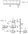
- Figure 4 illustrates an entry in a cache tag memory which is utilized by the present invention.
- a plurality of bits 50 labeled "Tag” correspond to the most significant bits of a memory location stored in a data cache entry.
- a bit 52 labeled "Status bit” is included in the tag and indicates whether or not an entry has been updated by a local processor.
- Other bits not shown in Figure 4 may also be included in the tag, examples being a snoop bit, a parity bit, and a valid bit.
- FIG. 5 an alternative high level block diagram illustrates a cache memory utilizing a cache tag memory according to the present invention.
- a cache tag RAM 54 and a data cache 56 communicate with system bus 26 and local processor 58 .
- Cache controller 60 performs the usual cache control functions found in caches which are suitable for use with single processor systems.
- a write enable signal (WE) in tag RAM 54 is utilized when data is transferred from main memory 62 into tag RAM 54 .
- a processor write enable signal (WE P ) in tag RAM 54 is used by local processor 58 to only alter the status bits stored in tag RAM 54 .
- the bits which make up the tag portion of the tag in other words the bits which are compared to determine a match, are controlled by the WE signal, while the status bit is controlled by both the WE signal and the WE P signal.
- Tag RAM 54 determines the correct first state of the status bit when the tag is initially written into tag RAM 54 , since the WE signal is enabled in order to set the status bit to the first state.
- the status bit may be altered during cache operations when the WE P signal is enabled by local processor 58 .
- the status bit is set to the second state only if a cache hit occurred while WE P is activated.
- only a data out pin is required for the status bits since the proper state of the status bits may be determined internally from the state of the WE signal, WE P signal, and the match pin.
- a input/output pin may be utilized for the status bits, however, and cache controller 60 can control the state of the status bits.
- cache controller 60 monitors the state of the status bit which corresponds to the entry which will be overwritten to see if the status bit has been set to a 1. If the status bit is set to a 1, the entry to be overwritten is written back to main memory before the new entry is stored in data cache 56 . If the status bit is set to a 0, the entry to be overwritten may be immediately replaced with the new entry.
- the approach described above requires cache controller 60 to monitor the status bits before altering data in data cache 56 .
- the status bits may be used as status flags.
- tag RAM 54 outputs a status flag. The status flag is set high only when the status bit is set to the second state and a cache miss occurs. The status flag indicates that data in data cache 56 must be written back to main memory 62 before it is replaced. This reduces the amount of logic required in cache controller 60 , because cache controller 60 is not required to monitor the status bits.
- Applicant has provided a cache tag memory for use in a copy back cache system which utilizes an internal status bit to indicate whether data has been altered in the cache memory but not in main memory. This results in a savings of board space because a separate memory for the status bits does not have to be provided in the cache memory. Additionally, the cache memory operates more efficiently, since information about the data in the cache memory is not stored in several memory arrays. This eliminates the need for the system to access several memory arrays to retrieve data and ascertain its integrity. Although the present invention has been described with reference to multi-processor systems, it is equally applicable to single processor systems.
Landscapes
- Engineering & Computer Science (AREA)
- Theoretical Computer Science (AREA)
- Physics & Mathematics (AREA)
- General Engineering & Computer Science (AREA)
- General Physics & Mathematics (AREA)
- Memory System Of A Hierarchy Structure (AREA)
Applications Claiming Priority (2)
| Application Number | Priority Date | Filing Date | Title |
|---|---|---|---|
| US98286292A | 1992-11-30 | 1992-11-30 | |
| US982862 | 1992-11-30 |
Publications (2)
| Publication Number | Publication Date |
|---|---|
| EP0604030A2 true EP0604030A2 (fr) | 1994-06-29 |
| EP0604030A3 EP0604030A3 (fr) | 1995-03-22 |
Family
ID=25529579
Family Applications (1)
| Application Number | Title | Priority Date | Filing Date |
|---|---|---|---|
| EP93309498A Withdrawn EP0604030A3 (fr) | 1992-11-30 | 1993-11-29 | Mémoire d'étiquettes pour antémémoire à post-mémorisation. |
Country Status (2)
| Country | Link |
|---|---|
| EP (1) | EP0604030A3 (fr) |
| JP (1) | JPH06222989A (fr) |
Cited By (2)
| Publication number | Priority date | Publication date | Assignee | Title |
|---|---|---|---|---|
| CN109478164A (zh) * | 2016-07-14 | 2019-03-15 | 超威半导体公司 | 用于存储用于高速缓存条目传输的高速缓存位置信息的系统和方法 |
| CN118349280A (zh) * | 2024-06-14 | 2024-07-16 | 北京微核芯科技有限公司 | 存数指令调度方法、装置、设备和存储介质 |
Families Citing this family (1)
| Publication number | Priority date | Publication date | Assignee | Title |
|---|---|---|---|---|
| CN113268384B (zh) * | 2021-04-30 | 2022-05-13 | 瑞芯微电子股份有限公司 | 一种标记空间异常检测方法及存储介质 |
-
1993
- 1993-11-29 EP EP93309498A patent/EP0604030A3/fr not_active Withdrawn
- 1993-11-29 JP JP5298443A patent/JPH06222989A/ja active Pending
Non-Patent Citations (2)
| Title |
|---|
| ELECTRICAL DESIGN NEWS vol. 37, no. 8 , May 1992 , NEWTON, MA, US page 74 XP000288050 R. QUINNELL 'Cache tag RAMs offer 12-nsec validated match with extras' * |
| ELECTRONIC DESIGN vol. 40, no. 7 , April 1992 , CLEVELAND, OH, US page 114 XP000329626 D. BURSKY 'Highly Integrated Cache-Tag RAMs Perform Matches In 12 NS' * |
Cited By (3)
| Publication number | Priority date | Publication date | Assignee | Title |
|---|---|---|---|---|
| CN109478164A (zh) * | 2016-07-14 | 2019-03-15 | 超威半导体公司 | 用于存储用于高速缓存条目传输的高速缓存位置信息的系统和方法 |
| CN109478164B (zh) * | 2016-07-14 | 2024-04-16 | 超威半导体公司 | 用于存储用于高速缓存条目传输的高速缓存位置信息的系统和方法 |
| CN118349280A (zh) * | 2024-06-14 | 2024-07-16 | 北京微核芯科技有限公司 | 存数指令调度方法、装置、设备和存储介质 |
Also Published As
| Publication number | Publication date |
|---|---|
| EP0604030A3 (fr) | 1995-03-22 |
| JPH06222989A (ja) | 1994-08-12 |
Similar Documents
| Publication | Publication Date | Title |
|---|---|---|
| US5513335A (en) | Cache tag memory having first and second single-port arrays and a dual-port array | |
| EP0347040B1 (fr) | Système de mémoire de données | |
| US5056002A (en) | Cache memory for use with multiprocessor systems | |
| US6047357A (en) | High speed method for maintaining cache coherency in a multi-level, set associative cache hierarchy | |
| US4847804A (en) | Apparatus and method for data copy consistency in a multi-cache data processing unit | |
| US5249284A (en) | Method and system for maintaining data coherency between main and cache memories | |
| EP0777183B1 (fr) | Système d'ordinateur à antémémoire | |
| US6981106B1 (en) | System and method for accelerating ownership within a directory-based memory system | |
| KR100273039B1 (ko) | 멀티프로세서 데이터 처리 시스템의 캐쉬 일관성을 유지하기위한 캐쉬 일관성 프로토콜 제공 방법 및시스템 | |
| US5530833A (en) | Apparatus and method for updating LRU pointer in a controller for two-way set associative cache | |
| US6065099A (en) | System and method for updating the data stored in a cache memory attached to an input/output system | |
| US5590307A (en) | Dual-port data cache memory | |
| US7325102B1 (en) | Mechanism and method for cache snoop filtering | |
| US4419725A (en) | Cache/disk subsystem with tagalong copy | |
| EP0474450A2 (fr) | Système de processeur avec des moyens de transfert de mémoire | |
| US6151661A (en) | Cache memory storage space management system and method | |
| EP0533427B1 (fr) | Système de commande de mémoire d'ordinateur | |
| US5367659A (en) | Tag initialization in a controller for two-way set associative cache | |
| US5737568A (en) | Method and apparatus to control cache memory in multiprocessor system utilizing a shared memory | |
| US6000017A (en) | Hybrid tag architecture for a cache memory | |
| EP0439952A2 (fr) | Mémoire d'étiquettes d'antémémoire à double porte | |
| US6256710B1 (en) | Cache management during cache inhibited transactions for increasing cache efficiency | |
| US6594732B1 (en) | Computer system with memory system in which cache memory is kept clean | |
| JPH04336641A (ja) | 処理システムにおける使用のためのデータキャッシュおよび方法 | |
| EP0604030A2 (fr) | Mémoire d'étiquettes pour antémémoire à post-mémorisation |
Legal Events
| Date | Code | Title | Description |
|---|---|---|---|
| PUAI | Public reference made under article 153(3) epc to a published international application that has entered the european phase |
Free format text: ORIGINAL CODE: 0009012 |
|
| AK | Designated contracting states |
Kind code of ref document: A2 Designated state(s): DE FR GB IT |
|
| PUAL | Search report despatched |
Free format text: ORIGINAL CODE: 0009013 |
|
| AK | Designated contracting states |
Kind code of ref document: A3 Designated state(s): DE FR GB IT |
|
| 17P | Request for examination filed |
Effective date: 19950922 |
|
| 18W | Application withdrawn |
Withdrawal date: 19970806 |