EP0604040A1 - Optisches Signalidentifikationsverfahren - Google Patents
Optisches Signalidentifikationsverfahren Download PDFInfo
- Publication number
- EP0604040A1 EP0604040A1 EP93309694A EP93309694A EP0604040A1 EP 0604040 A1 EP0604040 A1 EP 0604040A1 EP 93309694 A EP93309694 A EP 93309694A EP 93309694 A EP93309694 A EP 93309694A EP 0604040 A1 EP0604040 A1 EP 0604040A1
- Authority
- EP
- European Patent Office
- Prior art keywords
- optical
- wavelength
- signal
- optical signal
- individual
- Prior art date
- Legal status (The legal status is an assumption and is not a legal conclusion. Google has not performed a legal analysis and makes no representation as to the accuracy of the status listed.)
- Withdrawn
Links
- 230000003287 optical effect Effects 0.000 title claims abstract description 97
- 238000000034 method Methods 0.000 title claims abstract description 12
- 238000001514 detection method Methods 0.000 claims 3
- 230000005540 biological transmission Effects 0.000 abstract description 7
- 238000010586 diagram Methods 0.000 description 4
- 239000013307 optical fiber Substances 0.000 description 4
- 238000012544 monitoring process Methods 0.000 description 2
- 230000037361 pathway Effects 0.000 description 2
- 238000004891 communication Methods 0.000 description 1
- 230000007812 deficiency Effects 0.000 description 1
- 230000003111 delayed effect Effects 0.000 description 1
- 230000000694 effects Effects 0.000 description 1
- 230000007613 environmental effect Effects 0.000 description 1
- 238000000926 separation method Methods 0.000 description 1
- 230000007704 transition Effects 0.000 description 1
Images


Classifications
-
- H—ELECTRICITY
- H04—ELECTRIC COMMUNICATION TECHNIQUE
- H04B—TRANSMISSION
- H04B10/00—Transmission systems employing electromagnetic waves other than radio-waves, e.g. infrared, visible or ultraviolet light, or employing corpuscular radiation, e.g. quantum communication
- H04B10/60—Receivers
- H04B10/66—Non-coherent receivers, e.g. using direct detection
- H04B10/67—Optical arrangements in the receiver
-
- H—ELECTRICITY
- H04—ELECTRIC COMMUNICATION TECHNIQUE
- H04J—MULTIPLEX COMMUNICATION
- H04J14/00—Optical multiplex systems
- H04J14/02—Wavelength-division multiplex systems
-
- H—ELECTRICITY
- H04—ELECTRIC COMMUNICATION TECHNIQUE
- H04B—TRANSMISSION
- H04B10/00—Transmission systems employing electromagnetic waves other than radio-waves, e.g. infrared, visible or ultraviolet light, or employing corpuscular radiation, e.g. quantum communication
- H04B10/60—Receivers
- H04B10/66—Non-coherent receivers, e.g. using direct detection
- H04B10/67—Optical arrangements in the receiver
- H04B10/671—Optical arrangements in the receiver for controlling the input optical signal
- H04B10/675—Optical arrangements in the receiver for controlling the input optical signal for controlling the optical bandwidth of the input signal, e.g. spectral filtering
Definitions
- the invention relates to the optical transmission of information and, more particularly, to improving signal demultiplexing within a wavelength-multiplexed optical transmission system.
- optical signals within wavelength-multiplexed optical transmission systems several encoded optical signals (referred to as "channels"), each having a different wavelength, are transmitted simultaneously along a single optical path (typically an optical fiber). At the receiving end of such a system, the optical signals are separated (“demultiplexed”), and individually decoded.
- the above problem of drift can be corrected for by continually monitoring and adjusting the optical sources and receiving filters.
- correction measures prove expensive as a result of labor costs (if they are manually implemented), or as a result of increased hardware costs (if they are automatically implemented via active feedback loops).
- the monitoring and adjusting of the sources and filters does not offer a practical solution to the problems associated with wavelength drift within a wavelength-multiplexed optical transmission system.
- the present invention overcomes the deficiencies of prior wavelength-multiplexed optical signal identification techniques by modulating each of the individual channels within a multiplexed signal at a unique low-frequency. This modulation is performed at the transmission site of the optical signal, and the specific frequencies of modulation are chosen to be very much lower than the low-frequency cut-off of any other information encoded upon the optical signals.
- the invention directs each of the individual optical signals, as a function of the particular low-frequency modulation evident upon each signal, to a particular tunable Fabry-Perot ("FP") optical filter.
- FP filters have the ability to track the frequency of an individual channel, problems associated with wavelength drift are eliminated.
- FP filters offer a very narrow optical passband, allowing inter-channel cross-talk and noise levels to be minimized within wavelength-multiplexed optical systems employing the signal identification technique.
- a wavelength-multiplexed optical signal comprised of three individual optical component signals having wavelengths of ⁇ i, x 2 , and ⁇ 3 , is transmitted from a source to a receiver via an optical fiber.
- Each of these individual component signals, within the wavelength-multiplexed optical signal is amplitude modulated at a unique low-frequency -- f 1 , f 2 , and f 3 , respectively.
- This low-frequency amplitude modulation is independent of, and in addition to, any other modulation of the optical signals (such as high-frequency digital or analog information encoding). Any one of a number of well-known techniques for amplitude modulating an optical signal may be employed to effect the low-frequency modulation of the individual component optical signals.
- One such technique employs alternating waveforms of frequencies f 1 , f 2 and f 3 to modulate the bias current of each of the lasers producing the individual optical signals. While the specific low-frequency modulation technique is immaterial, the modulation frequencies must be very much lower than the low-frequency cut-off of any receiver coupled to the optical fiber for purposes of decoding high-frequency digital or analog information. This ensures that the reception of any high-frequency information carried by the optical component signals will not be interfered with as a result of the low-frequency modulation.
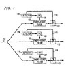
- FIG. 1 shows a simplified block diagram of a receiver which employs the invention to demultiplex a wavelength-multiplexed optical signal, in which each of the individual optical signals are low-frequency modulated as described above.
- the pathways illustrated as dotted lines in FIG. 1 carry optical signals, and the pathways illustrated as solid lines carry electrical signals.
- the wavelength-multiplexed optical signal traveling along optical fiber 101 is split, and input to three independently tunable FP filters (102, 103, and 104). Each FP filter is scanned over range of wavelengths, including ⁇ 1 , X 2 , and ⁇ 3 . This scanning is accomplished via associated FP filter controllers ("FPCs”), labeled as 105, 106, and 107 in FIG. 1.
- FPCs FP filter controllers
- the optical output of the tunable FP filters fluctuate as the passband of each FP filter is scanned over the range of wavelengths, with each optical output peaking as the passband of a given FP filter is tuned to the fundamental wavelength of any one the three component signals of the input optical signal.
- Optical splitter/sensors 111, 112, and 113 are shown to be coupled to the output of each FP filter. These splitter/sensors each produce an electrical signal proportional to the optical output of an associated FP filter. These electrical signals are each transmitted (via lines 114, 115, and 116) to a detector circuit (108, 109, and 110). Each of these detector circuits serves to detect a particular one of the three component optical signals, and cause the associated FPC and FP filter to phase-lock onto that optical signal.
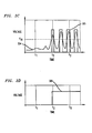
- FIG. 2 shows, in simplified form, a schematic diagram of detector circuit 109 (see FIG. 1).
- the circuit detects the presence of one particular multiplexed optical signal which is modulated at the specific low-frequency f 2 , and enables FP filter 103 to phase-lock onto the optical component signal having the fundamental wavelength of X 2 .
- the circuit of FIG. 2 includes bandpass filter 201, amplifier 202, comparators 203 and 204, buffer 205, and flip-flop 206.
- the positive input of comparator 204 receives an electrical signal from line 115. This signal is proportional to the optical output of FP filter 103 (FIG. 1). The output of comparator 204 attains a positive value when the amplitude of the signal upon line 115 exceeds that of reference voltage V R1 .
- the value of V R1 is fixed at a level which allows the output of comparator 203 to attain a positive value whenever the electrical input signal upon line 115 increases in response to the FP filter 103 (FIG. 1) peaking as FP filter 103 is scanned across wavelengths ⁇ 1 , x 2 , and ⁇ 3 .
- FIG. 3A provides a graphical illustration (amplitude versus time) of the signal which would be evident upon line 115 if FP filter 103 (FIG. 1) were freely scanned across a band including wavelengths ⁇ 1 , X 2 , and ⁇ 3 .
- FP filter 103 is tuned to wavelength ⁇ 1 at t 1 , to wavelength X 2 at t 2 , and to wavelength X 3 at t 3 .
- FIG. 3B provides a graphical illustration (amplitude versus time) of the signal upon line 115 (waveform 302), the output of comparator 204 (waveform 303), and the level of reference voltage V R1 , when FP filter 103 (FIG.
- bandpass filter 201 is adapted to pass electrical signals having a frequency of f 2 to amplifier 202.
- the amplified bandpass filtered signal output from amplifier 202 is then fed to the positive input of comparator 203.
- the output of comparator 203 attains a positive value when the amplitude of the input bandpass filtered signal exceeds that of reference voltage V R2 .
- the value of V R2 is fixed at sufficiently high level to cause the output of comparator 203 to attain a positive value only when a signal having a fundamental frequency of f 2 is being passed by filter 201.
- 3C provides a graphical illustration (amplitude versus time) of the signal output by bandpass filter 201 (waveform 304), the output of comparator 203 (waveform 305), and the level of reference voltage V R2 , and as FP filter 103 (FIG. 1) is scanned and phase-locked. As with FIG. 3B, the waveforms in FIG. 3C are not drawn to the same scale.
- the output of comparator 203 is a TTL signal on the order of 4 to 5 volts, while the level of V R2 is typically no more than several hundred millivolts.
- FIG. 2 the output of comparator 203 is fed to the data input of flip-flop 206, and to buffer 205.
- the signal from comparator 203 evident at the flip-flop data input serves to trigger the flip-flop, while the delayed pulse provided by buffer 205 serves as clock signal, thereby ensuring a stable transition by flip-flop 206.
- FIG. 3D provides a graphical illustration (amplitude versus time) of the signal 306 which is output by flip-flop 206. This output is fed to FPC 106 (FIG. 1).
- FPC 106 In response to receiving the output pulse from flip-flop 206 (FIG. 2), FPC 106 (FIG. 1) halts the wavelength scanning of FP filter 103, and places that FP filter into a phase-lock mode. Since detector circuit 109 ensures that the pulse output by flip-flop 206 coincides with passband of FP filter 103 being centered upon X 2 , FP filter 103 is locked onto the optical component signal having a wavelength of x 2 .
- Detector circuits 108 and 110 have configurations similar to that of detector circuit 109. However, the bandpass filter within detector circuit 108 is tuned to the frequency f 1 , and the bandpass filter within detector circuit 110 is tuned to the frequency f 3 . As a result, FPC 105 places FP filter 102 into a phase-lock mode when the passband of FP filter 102 is centered upon ⁇ 1 (as the component optical signal of wavelength ⁇ 1 is modulated at frequency f 1 ). Similarly, FPC 107 places FP filter 104 into a phase-lock mode when the passband of FP filter 104 is centered upon X 3 (as the component optical signal of wavelength X 3 is modulated at frequency f 3 ).
Landscapes
- Engineering & Computer Science (AREA)
- Computer Networks & Wireless Communication (AREA)
- Signal Processing (AREA)
- Physics & Mathematics (AREA)
- Electromagnetism (AREA)
- Spectroscopy & Molecular Physics (AREA)
- Optical Communication System (AREA)
Applications Claiming Priority (2)
| Application Number | Priority Date | Filing Date | Title |
|---|---|---|---|
| US99230892A | 1992-12-21 | 1992-12-21 | |
| US992308 | 1992-12-21 |
Publications (1)
| Publication Number | Publication Date |
|---|---|
| EP0604040A1 true EP0604040A1 (de) | 1994-06-29 |
Family
ID=25538167
Family Applications (1)
| Application Number | Title | Priority Date | Filing Date |
|---|---|---|---|
| EP93309694A Withdrawn EP0604040A1 (de) | 1992-12-21 | 1993-12-03 | Optisches Signalidentifikationsverfahren |
Country Status (3)
| Country | Link |
|---|---|
| EP (1) | EP0604040A1 (de) |
| JP (1) | JPH06222237A (de) |
| CA (1) | CA2104189A1 (de) |
Cited By (7)
| Publication number | Priority date | Publication date | Assignee | Title |
|---|---|---|---|---|
| EP0714182A3 (de) * | 1994-11-25 | 1996-11-27 | Pirelli Cavi Spa | Telekommunikationssystem und Verfahren zur Wellenlängenmultiplexübertragung mit geregelten Trennen von abgehenden Kanälen und zur Bestimmung des Signal-Rauschverhältnis |
| EP0763907A1 (de) * | 1995-07-31 | 1997-03-19 | PIRELLI CAVI S.p.A. | Wellenlängenmultiplex-Telekommunikationssystem mit geregelter Trennung abgehender Kanäle |
| US5917627A (en) * | 1995-06-17 | 1999-06-29 | Northern Telecom Limited | Optical TDM transmission system |
| EP0773640A3 (de) * | 1995-11-07 | 2000-05-10 | AT&T Corp. | Optisches Übertragungssystem mit hintereinander angeordneten Fabry-Perot Etalons zur Wellenlängenauswahl |
| WO2001054319A1 (en) * | 2000-01-17 | 2001-07-26 | The University Of Sydney | Method and apparatus for monitoring of data channels |
| AU781588B2 (en) * | 2000-01-17 | 2005-06-02 | University Of Sydney, The | Method and apparatus for monitoring of data channels |
| US8200091B2 (en) | 2007-07-02 | 2012-06-12 | Fujitsu Limited | Wavelength division multiplexing device and method of detecting input break of optical signal |
Citations (4)
| Publication number | Priority date | Publication date | Assignee | Title |
|---|---|---|---|---|
| US4841519A (en) * | 1987-06-26 | 1989-06-20 | Nec Corporation | Apparatus for discriminating an optical signal from others and an apparatus for tuning an optical wavelength filter used in the same |
| EP0381341A2 (de) * | 1989-01-27 | 1990-08-08 | AT&T Corp. | Frequenzumtastungsmoduliertes optisches System |
| US4989201A (en) * | 1987-06-09 | 1991-01-29 | At&T Bell Laboratories | Optical communication system with a stabilized "comb" of frequencies |
| US5144467A (en) * | 1989-07-28 | 1992-09-01 | Hitachi, Ltd. | Optical tuning method and apparatus suitable for selective reception of optical frequency division multiplex signals |
-
1993
- 1993-08-16 CA CA002104189A patent/CA2104189A1/en not_active Abandoned
- 1993-12-03 EP EP93309694A patent/EP0604040A1/de not_active Withdrawn
- 1993-12-20 JP JP5344606A patent/JPH06222237A/ja active Pending
Patent Citations (4)
| Publication number | Priority date | Publication date | Assignee | Title |
|---|---|---|---|---|
| US4989201A (en) * | 1987-06-09 | 1991-01-29 | At&T Bell Laboratories | Optical communication system with a stabilized "comb" of frequencies |
| US4841519A (en) * | 1987-06-26 | 1989-06-20 | Nec Corporation | Apparatus for discriminating an optical signal from others and an apparatus for tuning an optical wavelength filter used in the same |
| EP0381341A2 (de) * | 1989-01-27 | 1990-08-08 | AT&T Corp. | Frequenzumtastungsmoduliertes optisches System |
| US5144467A (en) * | 1989-07-28 | 1992-09-01 | Hitachi, Ltd. | Optical tuning method and apparatus suitable for selective reception of optical frequency division multiplex signals |
Cited By (13)
| Publication number | Priority date | Publication date | Assignee | Title |
|---|---|---|---|---|
| US5943147A (en) * | 1994-11-25 | 1999-08-24 | Pirelli Cavi S.P.A. | Telecommunication system and method for wavelength-division multiplexing transmissions with a controlled separation of the outgoing channels and capable of determining the optical signal/noise ratio |
| US5712716A (en) * | 1994-11-25 | 1998-01-27 | Pirelli Cavi S.P.A. | Telecommunication system and method for wavelength-division multiplexing transmissions with a controlled separation of the outgoing channels and capable of determining the optical signal/noise ratio |
| EP0714182A3 (de) * | 1994-11-25 | 1996-11-27 | Pirelli Cavi Spa | Telekommunikationssystem und Verfahren zur Wellenlängenmultiplexübertragung mit geregelten Trennen von abgehenden Kanälen und zur Bestimmung des Signal-Rauschverhältnis |
| US5808762A (en) * | 1994-11-25 | 1998-09-15 | Pirelli Cavi S.P.A. | Telecommunication system and method for wavelength-division multiplexing transmissions with a controlled separation of the outgoing channels and capable of determining the optical signal/noise ratio |
| GB2302484B (en) * | 1995-06-17 | 1999-08-04 | Northern Telecom Ltd | Optical tdm transmission system |
| US5917627A (en) * | 1995-06-17 | 1999-06-29 | Northern Telecom Limited | Optical TDM transmission system |
| US5793508A (en) * | 1995-07-31 | 1998-08-11 | Pirelli Cavi S.P.A. | Wavelength-division multiplexing telecommunication system and method providing a controlled separation of the output channels |
| EP0763907A1 (de) * | 1995-07-31 | 1997-03-19 | PIRELLI CAVI S.p.A. | Wellenlängenmultiplex-Telekommunikationssystem mit geregelter Trennung abgehender Kanäle |
| CN1078784C (zh) * | 1995-07-31 | 2002-01-30 | 光学技术美国公司 | 波分复用通信系统和提供输出信道可控制分离的方法 |
| EP0773640A3 (de) * | 1995-11-07 | 2000-05-10 | AT&T Corp. | Optisches Übertragungssystem mit hintereinander angeordneten Fabry-Perot Etalons zur Wellenlängenauswahl |
| WO2001054319A1 (en) * | 2000-01-17 | 2001-07-26 | The University Of Sydney | Method and apparatus for monitoring of data channels |
| AU781588B2 (en) * | 2000-01-17 | 2005-06-02 | University Of Sydney, The | Method and apparatus for monitoring of data channels |
| US8200091B2 (en) | 2007-07-02 | 2012-06-12 | Fujitsu Limited | Wavelength division multiplexing device and method of detecting input break of optical signal |
Also Published As
| Publication number | Publication date |
|---|---|
| JPH06222237A (ja) | 1994-08-12 |
| CA2104189A1 (en) | 1994-06-22 |
Similar Documents
| Publication | Publication Date | Title |
|---|---|---|
| EP0521514B1 (de) | Optisches Übertragungssystem mit Frequenzmultiplexierung | |
| US5239400A (en) | Technique for accurate carrier frequency generation in of DM system | |
| KR100247484B1 (ko) | 다채널 광원의 파장 및 광 세기를 안정화 시키기 위한 장치 및방법 | |
| EP0577036A1 (de) | Verfahren und Vorrichtung eines abstimmbaren Filters und optisches Kommunikationssystem unter Verwendung dieser Vorrichtung | |
| US20050002675A1 (en) | Method and apparatus for controlling modulator phase alignment in a transmitter of an optical communications system | |
| JPH08163097A (ja) | 光周波数多重用ロック装置 | |
| US20060056849A1 (en) | Long-distance synchronous transmission method using optical fibre | |
| US6512865B1 (en) | Cross-traffic suppression in wavelength division multiplexed systems | |
| EP0604040A1 (de) | Optisches Signalidentifikationsverfahren | |
| KR20030080251A (ko) | 광학적으로 증폭된 백업 수신기 | |
| GB1584317A (en) | Electronic time base error correction methods and arrangements | |
| CA1281367C (en) | Method and device for automatic frequency control of semiconductor lasers | |
| US20040114149A1 (en) | WDM channel monitor and wavelength locker | |
| US7212748B2 (en) | Frequency detection circuit, optical receiver and optical transmission system using the same | |
| US20060088321A1 (en) | Closed loop RZ-DPSK alignment for optical communications | |
| KR20010093388A (ko) | 고밀도 파장분할다중화 광통신 시스템의 광파장 제어 장치 | |
| US5491577A (en) | Tunable optical filter tuning device suitable for use in the receive part of an optical transmission system | |
| JP3720537B2 (ja) | 光伝送システムにおいて補助チャンネルを伝送するための方法 | |
| US5739937A (en) | Optical unit for restoring a pulse pattern, receiver suitable for use in a transmission system comprising such a unit | |
| EP0622913B1 (de) | Vorrichtung für optische Übertragung mit direkter Modulation des Senders und optischer Filterung beim Empfänger | |
| US4963744A (en) | Method and apparatus for providing accurate low noise demodulation | |
| US9203522B2 (en) | Phase lock loop control for digital communication systems | |
| JPH0685783A (ja) | 光fdm送信装置 | |
| JP2000092001A (ja) | 光送信装置 | |
| US20050175348A1 (en) | Synchronizer for rz-wdm signals and method for synchronization |
Legal Events
| Date | Code | Title | Description |
|---|---|---|---|
| PUAI | Public reference made under article 153(3) epc to a published international application that has entered the european phase |
Free format text: ORIGINAL CODE: 0009012 |
|
| AK | Designated contracting states |
Kind code of ref document: A1 Designated state(s): DE FR GB |
|
| STAA | Information on the status of an ep patent application or granted ep patent |
Free format text: STATUS: THE APPLICATION IS DEEMED TO BE WITHDRAWN |
|
| 18D | Application deemed to be withdrawn |
Effective date: 19941230 |