EP0604168A1 - Convertisseurs analogique-numeriques simultanés cascadables - Google Patents
Convertisseurs analogique-numeriques simultanés cascadables Download PDFInfo
- Publication number
- EP0604168A1 EP0604168A1 EP93310323A EP93310323A EP0604168A1 EP 0604168 A1 EP0604168 A1 EP 0604168A1 EP 93310323 A EP93310323 A EP 93310323A EP 93310323 A EP93310323 A EP 93310323A EP 0604168 A1 EP0604168 A1 EP 0604168A1
- Authority
- EP
- European Patent Office
- Prior art keywords
- analogue
- subreference
- signal
- digital
- signals
- Prior art date
- Legal status (The legal status is an assumption and is not a legal conclusion. Google has not performed a legal analysis and makes no representation as to the accuracy of the status listed.)
- Withdrawn
Links
- 239000002131 composite material Substances 0.000 claims 1
- 230000001419 dependent effect Effects 0.000 claims 1
- 230000000694 effects Effects 0.000 claims 1
- 239000003990 capacitor Substances 0.000 description 14
- 238000006243 chemical reaction Methods 0.000 description 13
- 238000010586 diagram Methods 0.000 description 3
- 238000005516 engineering process Methods 0.000 description 3
- 238000000034 method Methods 0.000 description 3
- 238000011144 upstream manufacturing Methods 0.000 description 2
- 230000000052 comparative effect Effects 0.000 description 1
- 230000001934 delay Effects 0.000 description 1
- 230000007704 transition Effects 0.000 description 1
- 238000009966 trimming Methods 0.000 description 1
Images


Classifications
-
- H—ELECTRICITY
- H03—ELECTRONIC CIRCUITRY
- H03M—CODING; DECODING; CODE CONVERSION IN GENERAL
- H03M1/00—Analogue/digital conversion; Digital/analogue conversion
- H03M1/12—Analogue/digital converters
- H03M1/14—Conversion in steps with each step involving the same or a different conversion means and delivering more than one bit
- H03M1/16—Conversion in steps with each step involving the same or a different conversion means and delivering more than one bit with scale factor modification, i.e. by changing the amplification between the steps
- H03M1/164—Conversion in steps with each step involving the same or a different conversion means and delivering more than one bit with scale factor modification, i.e. by changing the amplification between the steps the steps being performed sequentially in series-connected stages
- H03M1/165—Conversion in steps with each step involving the same or a different conversion means and delivering more than one bit with scale factor modification, i.e. by changing the amplification between the steps the steps being performed sequentially in series-connected stages in which two or more residues with respect to different reference levels in a stage are used as input signals for the next stage, i.e. multi-residue type
-
- H—ELECTRICITY
- H03—ELECTRONIC CIRCUITRY
- H03M—CODING; DECODING; CODE CONVERSION IN GENERAL
- H03M1/00—Analogue/digital conversion; Digital/analogue conversion
- H03M1/12—Analogue/digital converters
- H03M1/34—Analogue value compared with reference values
- H03M1/36—Analogue value compared with reference values simultaneously only, i.e. parallel type
- H03M1/361—Analogue value compared with reference values simultaneously only, i.e. parallel type having a separate comparator and reference value for each quantisation level, i.e. full flash converter type
- H03M1/362—Analogue value compared with reference values simultaneously only, i.e. parallel type having a separate comparator and reference value for each quantisation level, i.e. full flash converter type the reference values being generated by a resistive voltage divider
- H03M1/365—Analogue value compared with reference values simultaneously only, i.e. parallel type having a separate comparator and reference value for each quantisation level, i.e. full flash converter type the reference values being generated by a resistive voltage divider the voltage divider being a single resistor string
Definitions
- This invention relates to analogue to digital converters and in particular but not exclusively to cascadable flash analogue to digital converters.
- this invention provides an analogue to digital converter for converting an analogue input signal which lies within an analogue input range, characterised in that said converter comprises a stack of comparator circuits each corresponding to a subrange of said analogue input range, wherein said converter is operable to provide a digital output signal defining the subrange containing said analogue input signal, and an analogue output signal or signals defining the position of said analogue input signal within said subrange, said analogue output signal or signals being derived from the inputs to said comparator circuits.
- this invention provides an analogue to digital converter for converting an analogue input signal which lies within an analogue input range, characterised in that said converter comprises:- a stack of comparator circuits each including two inputs and an output; input means for supplying said analogue input signal to said comparator circuits for comparison; subreference generating means for providing a scale of subreference signals defining a plurality of subranges of said analogue input range and for supplying said subreference signals to corresponding comparator circuits; digital output means responsive to the output stages of said comparator circuits for providing a digital number corresponding to the subrange containing the analogue input signal, and analogue output means responsive to the states of the comparator circuits for providing an analogue output signal or set of signals which is or are derived from at least one of the subreference signals defining the subrange containing said analogue input signal, and which indicates the position of said analogue signal within said subrange.
- the analogue output signals for further conversion by the downstream converter are derived in analogue fashion from the analogue signals employed in the upstream converter and there is no back conversion of the digital output. Furthermore, the downstream converter is supplied with a signal or signals representing the position of the analogue input within the subrange rather than a comparison of the analogue input signal and the digital to analogue converted result of the first digitisation.
- the analogue output signals may be in a variety of forms, depending in particular on how the subreference signals are derived.
- the analogue output signals may include one or more of the following; a signal representing the lower limit of the analogue input range, and a signal representing the upper limit of the analogue input range.
- the analogue to digital converter preferably includes means for receiving reference signals defining the upper and lower limits of the analogue input range.
- the subreference generating means preferably responds to the upper and lower limits to provide said subreference signals which divide the input range into a number of subranges corresponding to the number of comparator circuits. This division may be achieved in different ways.
- a voltage signal corresponding to the analogue input range is applied across a chain of resistive elements and a voltage signal from between each adjacent two resistive elements is supplied to a corresponding comparator circuit.
- each comparator circuit receives an upper and a lower subreference signal taken from either side of the corresponding resistive element and defining the bounds of the associated subrange.
- the comparator circuits preferably include logic circuitry which supplies to said analogue output means the upper and lower subreference signals of the active comparator circuit immediately above the highest comparative circuit "set".
- the logic circuitry preferably also flags said active comparator circuit for identifying the appropriate digital number to the output by said output means.
- the reference chain may be a chain of capacitive elements preferably with a switching arrangement for charging the capacitative elements in parallel and then connecting the elements in series.
- the capacitive elements are preferably charged with a divided input reference signal.
- the total voltage across the capacitors when in series should be kept close to the input reference voltage. This may be achieved by using an accurate voltage divider or using closed loop successive approximation during non-conversion time.
- the technique however is generic in that, for example, a 15 bit conversion could be produced using three 5-bit converters.
- the converter provides an 8 bit number which defines the position of the analogue signal within the analogue range, in terms of the subrange or quantum occupied by the analogue signal.
- the converter also provides a set of analogue output signals which indicates the position of the analogue signal within the subrange. This set of analogue output signals is amplified and then supplied to a further analogue to digital converter where it is converted to form the remaining 8 bits of the 16 bit word.
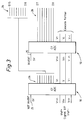
- the converter 10 comprises a stack of 255 comparator circuits 12 each comprising a differential amplifier 14.
- the non-inverting input of each amplifier 14 receives a common buffered input analogue signal (V in ), whilst the inverting input receives a respective subreference signal which is tapped from a reference chain 16 of resistors (R) connected between the top voltage reference (V +in ) and the bottom voltage reference (V -in ).
- the reference chain provides a scale of subreference signals which defines 255 equal subranges.
- each comparator circuit 12 is identified with a particular subrange of the analogue input range.
- the upper and lower subreference values defining the subrange of a particular comparator circuit are connected to upper and lower subreference rails 18, 20 via switching arrangements 22.
- the switching arrangements are operated by a logic circuit so that only the upper and lower subreference values of the subrange occupied by the signal are switched to the upper and lower subreference rails 18, 20. In other words, only the subreference values of the comparator circuit 12 immediately above the highest comparator circuit set are switched.
- the outputs 21 of all the comparator circuits 12 are supplied to corresponding input terminals 23 of an inverting priority encoder 24.
- the encoder 24 monitors those input terminals which are high and thereby provides at 26 an 8 bit word corresponding to the level of the analogue signal relative to the input range. This digital output indicates the eight most significant bits.
- an output set of three signals is provided as follows:
- V +out An output voltage (V +out ) equal to 256 times the difference between the upper active comparator element voltage and the lower active comparator element voltage.
- V out An output voltage (V out ) equal to 256 times the difference between the upper active comparator element voltage and the input signal.
- V -out A negative reference (V -out ) equal to the input negative reference voltage (buffered).
- V out goes down as the input volts (V in ) increase then the second cascade needs to invert the digital priority encoder, and this is done by applying an invert signal to the encoder 24 via invert terminal 25.
- invert signal to the encoder 24 via invert terminal 25.
- the analogue input signal supplied to the converter is fed to all the comparator circuits in parallel and each comparator compares the input signal with its subrange. If the analogue input is above the subrange the comparator sends to the encoder a high signal. Thus all the comparators in the stack corresponding to subranges below the analogue input will output high signals, and the comparator corresponding to the subrange containing the analogue input will output a low signal, as will all the comparators above that one.
- the low signal from the comparator whose subrange embraces the analogue input, and the high signal from the next lower comparator will make the logic circuitry close the transistor switches to supply analogue voltage levels corresponding to the upper and lower limits of the subrange to the analogue output stage for processing as detailed above.
- a resistor chain is used to generate the subreference voltages for each comparator.
- this reference chain could also be a series of capacitors, with a switching arrangement for charging to the subreferences in parallel from an accurately divided input reference. This arrangement is shown in Figure 2.
- the comparator circuits 42 are of similar form except that the subreference voltage is obtained from the capacitor chain 44 and also only the lower subreference value, i.e. that defining the lower limit of the subrange is supplied to the analogue output stage 46.
- the reference chain 44 includes a series of capacitors 47 disposed alternately with switching transistors 48. Across each capacitor 47 is applied a reference voltage via switching transistors 49. The switching transistors 48 are made conducting alternately with transistors 49 so that, during a calibration phase, the same reference is applied across each capacitor 47 in parallel. During a conversion phase, the transistors 48 are conducting so that they are in series.
- the common reference voltage applied across the capacitors is obtained by dividing the input reference voltage V ref+in by the number of comparator circuits, by adjusting the gain of buffer amplifier 50.
- each comparator is supplied via the common input 52 with the analogue input voltage. All those comparator circuits corresponding to subranges below the analogue input provide an output signal to the inverting priority encoder 54. As before, this provides a digital signal corresponding to the eight most significant bits.
- the comparator circuit immediately above the highest circuit “set” supplies via the logic switching circuit 56 its lower subreference value to the analogue output stage 46 via a lower subreference rail 58.
- the lower subreference value is subtracted from the analogue input signal to provide an analogue output signal V out to the next converter in the cascade.
- the analogue input reference signal defining the lower limit of the analogue input range (V ref-out ).
- This second embodiment does not require the generation of a reference output since the voltage on each capacitor is guaranteed to be equal, as they were all charged up in parallel. Instead the input reference could be used for all cascades.
- a possible disadvantage with this method is that some of the conversion cycle is required to switch the reference chain from serial to parallel to charge the subreference and then switch back to serial again.
- This could be overcome by the addition of a second bank of capacitors which would be regularly charged in parallel and then switched into series and connected to the main reference chain to equalise their voltages with the main reference chain so that the main reference chain could be used continuously, with only top up charging.
- the advantage with the capacitor version is that it would be more linear, since variations in capacitor values would not affect their charged voltage.
- the reference total should be kept as near as possible to the input reference. This can either be achieved by using an accurate voltage divider to generate the subreferences or by generating the subreferences as a closed loop successive approximation during non-convert time.
- two analogue to digital converters of the type shown in Figure 1 are cascaded together to provide an 16 bit converter.
- the output of the second 8 bit converter may be cascaded further if greater resolution is required.
- an analogue reference output set of signals (V +out and V -out ) is generated by measuring and amplifying the analogue voltages directly across the input resistor in the resistor chain relevant to the comparator immediately above the highest comparator set.
- an amplified analogue voltage (V out ) is generated which indicates the position of the analogue signal within the subrange defined by the particular comparator.
- the capacitor reference version uses as a cascade reference, the sum of the subreferences.
- an effective wide bit flash analogue digital converter design may be achieved using several orders of magnitude fewer circuit elements than conventional designs, and in so doing making the circuit a practical proposition with current technology.
Landscapes
- Engineering & Computer Science (AREA)
- Theoretical Computer Science (AREA)
- Analogue/Digital Conversion (AREA)
Applications Claiming Priority (2)
| Application Number | Priority Date | Filing Date | Title |
|---|---|---|---|
| GB9226608 | 1992-12-19 | ||
| GB929226608A GB9226608D0 (en) | 1992-12-19 | 1992-12-19 | Analogue to digital converters |
Publications (1)
| Publication Number | Publication Date |
|---|---|
| EP0604168A1 true EP0604168A1 (fr) | 1994-06-29 |
Family
ID=10726960
Family Applications (1)
| Application Number | Title | Priority Date | Filing Date |
|---|---|---|---|
| EP93310323A Withdrawn EP0604168A1 (fr) | 1992-12-19 | 1993-12-20 | Convertisseurs analogique-numeriques simultanés cascadables |
Country Status (2)
| Country | Link |
|---|---|
| EP (1) | EP0604168A1 (fr) |
| GB (1) | GB9226608D0 (fr) |
Cited By (3)
| Publication number | Priority date | Publication date | Assignee | Title |
|---|---|---|---|---|
| EP0741460A3 (fr) * | 1995-05-01 | 1998-01-07 | Thomson Consumer Electronics, Inc. | Circuit de référence pour les comparateurs dans un convertisseur analogique-numérique |
| DE10129013A1 (de) * | 2001-06-15 | 2003-01-02 | Infineon Technologies Ag | Schneller A/D-Wandler mit hoher Auflösung |
| US9081396B2 (en) | 2013-03-14 | 2015-07-14 | Qualcomm Incorporated | Low power and dynamic voltage divider and monitoring circuit |
Citations (4)
| Publication number | Priority date | Publication date | Assignee | Title |
|---|---|---|---|---|
| EP0262664A2 (fr) * | 1986-09-30 | 1988-04-06 | Kabushiki Kaisha Toshiba | Convertisseur analogique numérique |
| US4745393A (en) * | 1985-09-25 | 1988-05-17 | Hitachi, Ltd | Analog-to-digital converter |
| US4857931A (en) * | 1987-07-20 | 1989-08-15 | Zdzislaw Gulczynski | Dual flash analog-to-digital converter |
| US4929848A (en) * | 1989-01-31 | 1990-05-29 | Zdzislaw Gulczynski | High accuracy reference ladder |
-
1992
- 1992-12-19 GB GB929226608A patent/GB9226608D0/en active Pending
-
1993
- 1993-12-20 EP EP93310323A patent/EP0604168A1/fr not_active Withdrawn
Patent Citations (4)
| Publication number | Priority date | Publication date | Assignee | Title |
|---|---|---|---|---|
| US4745393A (en) * | 1985-09-25 | 1988-05-17 | Hitachi, Ltd | Analog-to-digital converter |
| EP0262664A2 (fr) * | 1986-09-30 | 1988-04-06 | Kabushiki Kaisha Toshiba | Convertisseur analogique numérique |
| US4857931A (en) * | 1987-07-20 | 1989-08-15 | Zdzislaw Gulczynski | Dual flash analog-to-digital converter |
| US4929848A (en) * | 1989-01-31 | 1990-05-29 | Zdzislaw Gulczynski | High accuracy reference ladder |
Cited By (4)
| Publication number | Priority date | Publication date | Assignee | Title |
|---|---|---|---|---|
| EP0741460A3 (fr) * | 1995-05-01 | 1998-01-07 | Thomson Consumer Electronics, Inc. | Circuit de référence pour les comparateurs dans un convertisseur analogique-numérique |
| AU713606B2 (en) * | 1995-05-01 | 1999-12-09 | Thomson Consumer Electronics, Inc | Analog-to-digital converter comparator reference arrangement |
| DE10129013A1 (de) * | 2001-06-15 | 2003-01-02 | Infineon Technologies Ag | Schneller A/D-Wandler mit hoher Auflösung |
| US9081396B2 (en) | 2013-03-14 | 2015-07-14 | Qualcomm Incorporated | Low power and dynamic voltage divider and monitoring circuit |
Also Published As
| Publication number | Publication date |
|---|---|
| GB9226608D0 (en) | 1993-02-17 |
Similar Documents
| Publication | Publication Date | Title |
|---|---|---|
| US4875048A (en) | Two-step parallel analog to digital converter | |
| US6600437B1 (en) | High resolution, high speed, low power switched capacitor digital to analog converter | |
| EP1917719B1 (fr) | Circuit de condensateur commute a tension de reference echelonnee | |
| US4533903A (en) | Analog-to-digital converter | |
| US5426431A (en) | Analog/digital converter | |
| US5184130A (en) | Multi-stage A/D converter | |
| US4647903A (en) | Successive approximation analog-to-digital converter | |
| US5210537A (en) | Multi-stage A/D converter | |
| US6229472B1 (en) | A/D converter | |
| US5572212A (en) | Pipelined analog to digital converter | |
| US7002507B2 (en) | Pipelined and cyclic analog-to-digital converters | |
| US5394148A (en) | AD converter | |
| JPH01136420A (ja) | 平衡入力を有するフラッシュコンバータによるサブレンジングa/dコンバータ | |
| Petschacher et al. | A 10-b 75-MSPS subranging A/D converter with integrated sample and hold | |
| JPH01136421A (ja) | 誤り補正を改良したサブレンジングa/dコンバータ | |
| US4559522A (en) | Latched comparator circuit | |
| US5313206A (en) | Sub-ranging analogue to digital converter using differential signals and direct current subtraction | |
| JPH0681048B2 (ja) | A/d変換器 | |
| US6288662B1 (en) | A/D converter circuit having ladder resistor network with alternating first and second resistors of different resistance values | |
| JP2995599B2 (ja) | アナログデジタル変換方法 | |
| EP0604168A1 (fr) | Convertisseurs analogique-numeriques simultanés cascadables | |
| EP0782790B1 (fr) | Convertisseur analogique/numerique permettant de generer un code de gray numerique a n bits | |
| US4633219A (en) | Integrable analog-to-digital converter | |
| US5629702A (en) | Analog to digital converter | |
| KR950010209B1 (ko) | 병렬형 a/d 콘버터의 직선성 보상회로 |
Legal Events
| Date | Code | Title | Description |
|---|---|---|---|
| PUAI | Public reference made under article 153(3) epc to a published international application that has entered the european phase |
Free format text: ORIGINAL CODE: 0009012 |
|
| AK | Designated contracting states |
Kind code of ref document: A1 Designated state(s): BE DE ES FR GB IT SE |
|
| RAP1 | Party data changed (applicant data changed or rights of an application transferred) |
Owner name: MMS SPACE SYSTEMS LIMITED |
|
| STAA | Information on the status of an ep patent application or granted ep patent |
Free format text: STATUS: THE APPLICATION IS DEEMED TO BE WITHDRAWN |
|
| RAP1 | Party data changed (applicant data changed or rights of an application transferred) |
Owner name: MMS SPACE SYSTEMS LIMITED |
|
| 18D | Application deemed to be withdrawn |
Effective date: 19941230 |