EP0605401B1 - Système à calculateur parallèle utilisant une méthode SIMD - Google Patents
Système à calculateur parallèle utilisant une méthode SIMD Download PDFInfo
- Publication number
- EP0605401B1 EP0605401B1 EP94104303A EP94104303A EP0605401B1 EP 0605401 B1 EP0605401 B1 EP 0605401B1 EP 94104303 A EP94104303 A EP 94104303A EP 94104303 A EP94104303 A EP 94104303A EP 0605401 B1 EP0605401 B1 EP 0605401B1
- Authority
- EP
- European Patent Office
- Prior art keywords
- address
- data
- signal
- processor
- controller
- Prior art date
- Legal status (The legal status is an assumption and is not a legal conclusion. Google has not performed a legal analysis and makes no representation as to the accuracy of the status listed.)
- Expired - Lifetime
Links
Images


Classifications
-
- G—PHYSICS
- G06—COMPUTING OR CALCULATING; COUNTING
- G06F—ELECTRIC DIGITAL DATA PROCESSING
- G06F15/00—Digital computers in general; Data processing equipment in general
- G06F15/76—Architectures of general purpose stored program computers
- G06F15/80—Architectures of general purpose stored program computers comprising an array of processing units with common control, e.g. single instruction multiple data processors
- G06F15/8007—Architectures of general purpose stored program computers comprising an array of processing units with common control, e.g. single instruction multiple data processors single instruction multiple data [SIMD] multiprocessors
- G06F15/8023—Two dimensional arrays, e.g. mesh, torus
Definitions
- the present invention relates to a parallel computer system using a SIMD method constituted by a controller and a plurality of processor elements connected to each other in a lattice configuration.
- Parallel computer systems are widely used, particularly, in the field of CAD (Computer Aided Design) which necessitates high speed calculation for a LSI (large scale integrated) circuit design. Accordingly, it is necessary to improve techniques to make these processor elements operate more efficiently in accordance with requirements of high density and high speed LSI.
- CAD Computer Aided Design
- MIMD multiple instruction stream multiple data stream
- processor elements are connected to a corresponding controller, respectively. Accordingly, it is necessary to provide the same number of controllers as there are processors.
- controllers are necessary in accordance with the number of processors, which can be from several tens to several hundreds of processors.
- the other method is called an SIMD (single instruction stream multiple data stream) method which is constituted by a plurality of processor elements and one controller.
- the controller is connected in parallel to all processor elements. Accordingly, it is possible to constitute a large scale parallel computer which has a large number of processor elements, for example, tens of thousands of processors.
- WO-A-88/04076 by Thinking Machines Corporation discloses a parallel computer system according to the preamble of accompanying claim 1.
- a parallel computer system using a SIMD method constituted by a controller and a plurality of processor elements, each of said processor elements having an internal storage means to store data to be processed and an external memory to store read and write data, said controller controlling operation of said processor elements, and said parallel computer system performing processing of said data based on a calculation control signal transmitted from said controller, characterised in that said parallel computer system comprises: a plurality of control groups, each of said control groups being constituted by a number of processor elements divided from a plurality of said processor elements, for use as an address control unit; a plurality of scheduling means, each of said scheduling means provided for one of said control groups and operatively connected to said controller, and for receiving and managing an event signal designating an address signal for data to be processed and transmitted from an adjacent control group, wherein a memory space of said external memory is divided into a plurality of windows of virtual processor elements each comprising a virtual processing element address as a relative address, and each window having a window number as a base address, and where
- a parallel computer system can control all processor elements so as to effectively and uniformly distribute the processor elements as a load.
- Embodiments of the present invention may provide a parallel computer system using a SIMD method enabling high efficiency data processing and high load distribution capability.
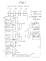
- Figure 1 is a basic block diagram of one type of parallel computer system useful for understanding the invention, as background information.
- reference number 10 denotes a controller, 11 a control memory for storing a micro-code including output control signals, and 12 a global data register for performing an input/output operation of the data processed or to be processed.
- the control memory 11 and the global data register 12 are provided in the controller 10.
- Reference number 13 denotes a data collection circuit for collecting output data from processor elements (PE) 14.
- 15A to 15D denote control registers CR constituting a calculation control circuit and connected to each other using a pipe-line method for applying various calculation control signals to the collection circuit 13.
- 16A to 16D denote gathering logic units (GLU) constituting the collection circuit 13 and each constituted by a tree configuration.
- Reference number 17 denotes a signal line for the calculation control signal to the GLU, 18 a signal line for controlling processor elements, and 19 a data line for broadcasting global data.
- Each of the processor elements comprises a data register for storing the data to be processed and an arithmetic logic unit ALU as shown in Fig. 3.
- the arithmetic logic unit ALU calculates the data stored in the register in response to the order transmitted from the controller 10 through the signal line 18.
- Each gathering logic unit GLU 16A to 16D collects the output data transmitted from the processor elements.
- the gathering logic units 16A to 16D are connected in the form of a tree configuration having several stages. That is, in Fig. 1, the units 16A are the first stage, the units 16B are the second stage, and the unit 16D is the final stage.
- the outputs of the processor elements 14 are input to the gathering logic units 16A.
- the resultant calculation data obtained in the GLU's 16A are output to the GLU's 16B.
- the resultant data obtained in the GLU's 16B are output to the next stage.
- the final stage 16D gathers all resultant data obtained in the previous stages and the data calculated in the final stage 16D is output to the global data register 12 in the controller 10.
- Each of the calculation control registers CR 15A to 15D are connected in series with each other using the pipe-line method.
- the number of registers is equal to the number of stages in the gathering logic unit GLU.
- the calculation in each stage is performed in response to the calculation control signals, for example, an "ADD" calculation signal, transmitted through the signal line 17. That is, when the calculation signal "ADD" is input to the first stage 16A, the calculation suggested by the calculation signal is performed in the first stage 16A regarding the data output from the processor elements. This calculation signal is transmitted to the next stage in response to the clock signal from the controller 10 and the same calculation suggested by the calculation signal is performed in the second stage 16B.
- the above calculation is performed using the pipe-line method. That is, when the first calculation signal "ADD" is input to the first stage, the next calculation signal, for example, "MAX" is input to the first stage.
- the synchronization of all processor elements is performed in accordance with a synchronization signal from the controller 10.
- the controller 10 sends the synchronization signal to all processor elements through the control line 18 to output the value "1" when each processor element completes the predetermined processing.
- the signal "AND" is transmitted to the control register 15A through the control line 17.
- the GLU 16A of the first stage performs an "AND” calculation regarding all output from the processor element in response to the first clock.
- the same “AND” calculation is performed in the GLU 16B of the next stage in response to the next clock.
- the controller 10 can recognize that all processor elements output the value "1".
- the essential processor element having the essential data is extracted as follows.
- a proper processor number is previously attached to each processor element.
- the controller 10 commands the essential processor element to output the proper number.
- the controller 10 commands another processor element to output a suitable signal, for example, the value "11---1" or "00---0".
- the controller 10 then sends the control signal "MAX” or "MIN" to the control register 15A.
- the essential processor element can be selected in response to "MAX" or "MIN" of the number in the collection circuit 13.
- a next essential processor element can be selected from the remaining processor elements excluding the first essential processor element in the same manner as the above. Accordingly, it is possible to use this circuit to select the priority order of use of a bus line.
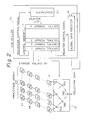
- Figure 2 illustrates one particular version of the system shown in Fig. 1.
- reference number 20 denotes a processor array the elements of which are connected to each other in a lattice configuration.
- the processor array and the collection circuit are controlled by the control signals from the controller 10.
- the control memory 11 in the controller 10 comprises a plurality of control formats 1 to n.
- the controller 10 further comprises a sequencer 21 which determines the sequence for reading out the control information from the control memory 11.
- the global data register 12 is a register for holding the data transmitted in common to all processor elements and to receive the output data from the collection circuit 13.
- FIG. 3 is a schematic block of a processor element.
- reference number 30 denotes a data register for holding the data to be processed.
- 31 denotes an arithmetic logic unit ALU for calculating the data stored in the register 30.
- the processor element 14 is controlled by the same control signal transmitted from the controller 10. This control signal includes an address of the data register 30 and an operation code for the arithmetic logic unit 31.
- the processor element 14 further comprises four ports, i.e., east port (E), west port (W), north port (N) and south port (S) for communicating between adjacent processor elements.
- the processor element 14 further comprises an input terminal GT for inputting the data from the global data register 12, and a collection terminal CT for outputting the data.
- the processor element 14 is a one-bit type and the input/output operation to the data register 30 is basically performed for each bit. Data larger than one bit is processed from the most significant bit (MSB) or the least significant bit (LSB) for each bit.
- MSB most significant bit
- LSB least significant bit
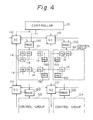
- FIG. 4 is a basic block diagram showing a type of parallel computer system embodying the present invention.
- reference number 110 denotes a scheduling circuit SC, 120 a real address generation circuit RAGC, and 150 a pseudo processor element.
- G1 to G4 denote control groups to be used as a control unit for accessing the address. Accordingly processor elements are divided into several control groups.
- the scheduling circuit 110 and the real address generation circuit 120 are provided for each control group.
- the scheduling circuit 110 is a circuit for receiving an event signal to designate the address and for managing the address designated by the event signal by using a queue.
- the real address generation circuit 120 is a circuit for generating a real address of the data to be processed by the processor element belonging to that control group. This generation is performed based on a base address determined by the event signal and an address signal applied from the controller 10.
- the pseudo processor element 150 is provided in the boundary portion of each control group.
- the pseudo processor element 150 has a function of sending the data corresponding to the address of the processor element when the processor element located to the boundary portion gives and takes the data between the adjacent processor elements belonging to the adjacent control group. This circuit is provided to ensure consecutiveness between the processor elements.
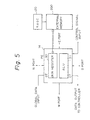
- FIG. 5 is a schematic block diagram of a processor element shown in Fig. 4. This drawing is the same as Figure 3 except that an external memory 200 is added between the data register 30 and the real address generation circuit 120. The address of the external memory 200 is applied from the real address generation circuit 120 provided in every control group.
- This type of parallel computer system embodying the invention mainly relates to the address control for the external memory 200.
- Figure 6 is a view for explaining the concept of the type of system shown in Fig. 4.
- Reference number 301 denotes an actual processor element group, 302 a first memory space corresponding to the actual processor element group 301, and 300 a second memory space (virtual area) corresponding to a virtual processor element group.
- the first memory space 302 coincides with an object area to be processed by the actual processor element group 301.
- the object area to be processed (for example, a wire pattern area) coincides with the size of the actual processor element group.
- the object area can be widened up to the second memory space.
- the actual processor element group 301 moves to the second memory space 300 so that it is possible to process data regarding the larger object area exceeding the first memory space. Therefore, although the virtual processor element group does not actually exist it is possible to obtain the same performance as the processor element group having the second memory space 300 by moving the actual processor element group 301.
- Figure 7 is a view for explaining division of the virtual area shown in Fig. 6.
- the second memory space 300 is divided into a plurality of windows (m x n window). Accordingly, one window corresponds to the first memory space 302 processed by the actual processor element group 301.
- the window number is attached to each window from 0 to nm-1, respectively.
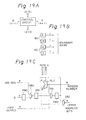
- Figures 8A and 8B are views for explaining addresses of memory spaces.
- the external memory 200 of one processor element 14 is divided into sixteen memory spaces for the virtual processor element. That is, "0000" to "FFFF” are addresses for the external memory each having sixteen bits, while “000” to “FFF” are addresses for the virtual area each having twelve bits. Accordingly, one actual processor element functions as sixteen virtual processor elements.
- the window number denotes the base address indicating the head of each memory space of the virtual PE (processor element) and constituted by eight bits "aaaa 0000" since a maximum of 256 windows can be provided. Since the external memory 200 is divided into sixteen blocks in this embodiment, the lower four bits are set to "0000".
- the virtual PE address "0000 bbbbbbbbbbb” denotes the relative address of each memory space of the virtual PE.
- the virtual PE address is transmitted in common to all processor elements from the controller 10.
- the virtual PE address has "0000" in the upper bits in accordance with the number of the window.
- the virtual PE address is constituted by twelve bits.
- the real address "aaaabbbbbbbbbbbbbbbb” having sixteen bits of the external memory 200 can be obtained by adding (or performing an OR operation) the base address and the virtual PE address.
- the processing of the data in the virtual PE is performed in such a way that the real PE sequentially processes the corresponding data in the virtual memory space divided from the real external memory 200.
- the real PE always sequentially processes all virtual PE's including its own external memory.
- this method is not efficient because the virtual PE's in which the processing is not necessary are included. Accordingly, the present invention selects the virtual PE's in which the processing is necessary so that the efficiency of the processing can be raised. Therefore, the concept of the "event" is employed to realize this method in the invention.
- the event is started when the conditions to be processed to the virtual PE are realized.
- the virtual PE which received the event is handled as the object to be processed by the real PE.
- the controller determines the content of the event in accordance with a program.
- FIG. 9 is a view for explaining control groups shown in Fig. 4.
- the processor elements (PE) 14 are divided into the control groups G1, G2, ---.
- the PE's of 128 x 128 are divided into sixteen control groups G1 to G16 each having 32 x 32 PE's.
- FIG. 10 is a block diagram of control groups and peripheral circuits.
- G1 to G16 are control groups
- 110 (SC) is the scheduling circuit provided for each control group
- 120 is a real address generation circuit also provided for each control group.
- the scheduling circuit 110 receives the event from the PE and manages the virtual PE to be processed.
- the virtual PE number to be processed i.e., the window number, is queued in the scheduling circuit 110 and sequentially processed from the head of the queue.
- the scheduling circuit 110 sends the base address corresponding to the virtual PE to the real address generation circuit 120. Accordingly, the scheduling circuit 110 performs the queueing and assigns the real PE.
- the real address generation circuit 120 generates the real address based on the relative address of the virtual PE and the base address.
- the relative address indicates a kind of control signal transmitted in common from the controller to all PE's, and the base address is determined by the scheduling circuit 110.
- the real address is transmitted to the real PE's in each control group.
- the scheduling circuit 110 is connected to four adjacent scheduling circuits. Each input/output signal is explained below.
- Event signal (as input signal)
- This event signal is obtained by the OR logic among the event signals transmitted from all PE's (32 PE's in this embodiment) located on the boundary of the control group, and is used as the input signal.
- This signal is one bit for four directions of E, W, N, and S.
- the window number signal of the adjacent scheduling circuit 110 is input as the input signal.
- the window number signal has eight bits as shown in Fig. 8B for four directions of E, W, N, and S.
- the scheduling circuit inputs the corresponding window number to the event signal when that event signal is activated, and performs the queuing.
- This signal is obtained by the OR logic among all event signals of the PE's included in its own control group, and has one bit.
- This signal is the window number signal output to the adjacent scheduling circuit 110, and has eight bits for four directions of E, W, N, and S.
- This signal is an output signal to the real address generation circuit 120 indicating the corresponding address to the window number of the virtual PE read-out from the head of the queue.
- control signal NEXT is a signal to indicator reading out a next virtual PE from the queue
- control signal DIR is a signal to indicate the direction of the data flow in four directions E, W, N, and S.
- the control signal EMPTY is a signal to indicate vacancy of the input signal, the clock signal, and the queue.
- Figure 11 is a block diagram for explaining the pseudo processor element (PE) shown in Fig. 4.
- the boundary BD of the control group is provided between the processor elements 8A and 8B. That is, the PE 14A is adjacent to the PE 14B.
- the pseudo PE (PS-PE) 150A is provided adjacent to the PE 14A, and the pseudo PE 150B is provided adjacent to the PE 14B, respectively.
- the pseudo PE is provided for ensuring the consecutiveness of the processing between adjacent control groups. This is because the adjacent control group can not receive the necessary value of the window when the object window between the adjacent control groups is different. Accordingly, as shown in Figs. 4 and 11, the pseudo PE is provided to each end of the row of the PE's in each control group. Therefore, when the object window is consecutive between adjacent control groups, the pseudo PE's are not used and the PE 14A directly accesses the PE 14B by switching the selectors S1 and S2.
- the write data is simultaneously written to the external memory 200a belonging to the pseudo PE 150A.
- the pseudo PE 150A read the data from the external memory 200a and transmits that data to the PE 14B through the selector S1 instead of the PE 14A.
- the address of the external memory 200a is the window address of the PE 14B side. The same operation as the above is performed in case of the data transmission from the PE 14B to the PE 14A.
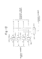
- Figure 12 is a detailed block diagram of the scheduling circuit shown in Fig. 4 and Figures 13 to 19 are detailed circuits of the diagram in Fig. 12.
- reference number 500 denotes an input circuit for the window number
- 510 a registration table
- 520 a consecutiveness detection circuit
- 530 an input circuit for the event
- 540 an event interpretation circuit
- 550 a first-in/first-out (FIFO) circuit
- 560 a registration flag circuit
- 570 an address holding circuit
- 580 an address calculation circuit.
- R1 to R4 denote registers for the pipe-line control.
- the input circuit 500 inputs the window number determined from the four adjacent directions E, W, N, and S, where DIR is the control signal for indicating the data flow. This circuit is shown in detail in Fig. 13.
- R10 denotes a register for holding the window numbers input from four directions E, W, N and S.
- S10 denotes a selector for selecting the window number in response to the control signal DIR and outputting the selected window number having eight bits.
- the registration table 510 is a table for storing flags indicating whether or not the window number is registered. One bit is assigned to each window in a maximum of 256 windows. Accordingly, the window number from the input circuit 500 becomes the address in the table 510. Therefore, double registration of a window number is prevented by this method.
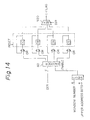
- the consecutiveness detection circuit 520 determines the consecutiveness between the present area and the adjacent area.
- the detailed circuit is shown in Fig. 14.
- COMP denotes a comparator, 600 an encoder (ECD), OR an OR circuit, and S20 a selector (SEL).
- CE, CW, CN and CS denote registers for storing the resultant data of the detection of the consecutiveness until the reset signal is input.
- the comparator COMP compares the upper bits of the address of its own control group with the window number input from the input circuit 500. When the former coincides with the latter, the encoder 600 outputs an enable signal in response to the direction control signal DIR.
- the enable signal is stored in the registers CE, CW, CN and CS as consecutiveness data and the consecutiveness data C-FLAG is output from the selector S20 in response to the control signal DIR.
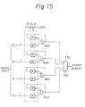
- the event input circuit 530 receives the event signals from four directions. The detailed circuit is shown in Fig. 15.
- EVCLR denotes an event clear signal to clear each register R.
- S30 denotes a selector circuit. The register R is cleared by the event clear signal EVCLR. When the event signal is loaded in the register R, the event signal is output from the selector S30 through the AND circuit.
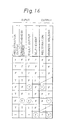
- the event interpretation circuit 540 judges whether or not the queuing of the window number should be performed, or whether or not the present address should be held.
- the detailed logic table for determining the output from this circuit 540 is shown in Fig. 16.
- T denotes an active state of the signals.
- the registration signal REG indicating the queuing of the window number is output from the circuit 540 only when the output of the input circuit 530 is active.
- the address holding signal AHS is output when the consecutiveness signal C-FLAG and the event signal are active. Further, the address holding circuit is output when the self-event signal is active.
- the FIFO 550 stores the window number to be processed in accordance with the event signal.
- the detailed circuit is shown in Fig. 17.
- MEM denotes a memory having the capacity of 8 x 256 bits, R40 to R43 registers, S40 a selector, WCNT a write counter to output the write address, RCNT a read counter to output the read address, and COMP a comparator.
- the registration signal is set in the register R41
- the window number stored in the register R40 is written to the address indicated by the write counter WCNT in the memory MEM.
- the content of the address of the memory MEM is read out in response to the control signal NEXT through the register R42 and the AND circuit, and output through the register R43.
- the comparator detects coincidence between the content of the write counter WCNT and the content of the read counter RCNT, a signal EMPTY indicating the vacant state is output.
- the registration flag circuit 560 is shown in detail in Fig. 18.
- 700 denotes an encoder, and R a register.
- the direction of the registered window number is stored in the register R after being encoded by the encoder 700 in accordance with the direction control signal DIR.
- the address calculation circuit 580 outputs the window number to be informed to the adjacent control group and the upper address bits used for generation of the real address based on the window number read out from the FIFO 550.
- the detailed circuit is shown in Figs. 19A to 19C.
- the control group sends the window numbers (A + 1) and (A - 1) for the horizontal direction, and sends the window numbers (A + B) and (A - B) for the normal direction, where B denotes the number of the window for the transverse direction when the virtual area is divided into the plural windows.
- the boundary of the window is distinguished by the boundary marks (E, W, N, S) 80.
- the value of each boundary mark is set by the controller 10 in the initial stage.
- ALU denotes calculation circuit, R80 to R82 registers, and S80 to S82 selectors.
- the calculation circuit ALU calculates any of the window numbers A, A ⁇ 1, and A ⁇ B in accordance with the boundary mark E, W, N, S shown in Fig. 19B.
- An address designation value ADD-DEG indicates a mode using the address transmitted from the controller 10 as an absolute address regardless of the present window number. When this mode is designated, the address designation value ADD-DEG is transmitted to the real address generation circuit 120 through the selectors S80 and S82.
- FIG. 20 is a detailed block diagram of the real address generation circuit.
- R100 to R105 denote registers, S100 to 103 selectors, and OR denotes OR circuits.
- the input signals to this circuit are the relative address of the virtual PE transmitted from the controller 10, the upper address bits output from the address calculation circuit 580, and the adjacent window numbers input from the input circuit 500.
- the real address to the PE belonging to its own control group is generated by adding the relative address set in the register R100 to the upper address bits set in the register R101 as shown in Fig. 8B. As shown in Fig. 8B, in the upper eight bits, when the base address and the relative address overlap, one side is set to "0".
- the real address is obtained by the logic OR calculation. In this case, the lower eight bits of the real address are the same bits as transmitted from the controller 10.
- the window number of the adjacent PE is set in the registers R102 to R105. Further, the window numbers are controlled by the selectors S100 to S103 to be the address of the adjacent control group when loading (L), and to be the self-address when saving (S).
- the multi-processor is constituted by lattice coupling, it is possible to constitute it by hyper-cubic coupling in accordance with the application.
Landscapes
- Engineering & Computer Science (AREA)
- Computer Hardware Design (AREA)
- Theoretical Computer Science (AREA)
- Computing Systems (AREA)
- Physics & Mathematics (AREA)
- General Engineering & Computer Science (AREA)
- General Physics & Mathematics (AREA)
- Multi Processors (AREA)
- Complex Calculations (AREA)
- Image Processing (AREA)
Claims (4)
- Système d'ordinateurs parallèles utilisant un procédé SIMD constitué par un dispositif de commande (10) et une pluralité d'éléments de processeur (14), chacun desdits éléments de processeur ayant un moyen de stockage interne (30) pour stocker des données à traiter et une mémoire externe (200) pour stocker des données de lecture et d'écriture, ledit dispositif de commande commandant le fonctionnement desdits éléments de processeur, et ledit système d'ordinateur parallèle réalisant le traitement desdites données sur la base d'un signal de commande de calcul transmis par ledit dispositif de commande, caractérisé en ce que ledit système d'ordinateur parallèle comprend :une pluralité de groupes de commande (G1, G2,...), chacun desdits groupes de commande étant constitué par un nombre d'éléments de processeur (14) divisé à partir d'une pluralité desdits éléments de processeur à utiliser comme une unité de commande d'adresse ;une pluralité de moyens de planification (110), chacun desdits moyens de planification prévus pour un desdits groupes de commande (G1, G2,...) et raccordé fonctionnellement audit dispositif de commande (10), et pour recevoir et contrôler un signal d'événement désignant une adresse relative pour des données à traiter et à transmettre à partir d'un groupe de commande adjacent, où un espace de mémoire de ladite mémoire interne (200) est divisée en une pluralité de fenêtres d'éléments de processeur virtuel comprenant chacun une adresse d'élément de traitement virtuel comme ladite adresse relative, et chaque fenêtre ayant un nombre de fenêtres comme adresse de base, et dans lequel ledit moyen de planification (110) détermine un élément de processeur virtuel dans lequel un traitement est nécessaire, sur la base de son numéro de fenêtre, en réponse audit signal d'événement ; etune pluralité de moyens de génération d'adresse réelle (120), chacun desdits moyen de génération d'adresse réelle prévu pour un desdits groupes de commande (G1, G2,...) et raccordé entre ledit dispositif de commande (10), ledit moyen de programmation (110), et ledit groupe de commande, pour générer un signal d'adresse réelle pour des données à traiter par un dit élément de processeur (14) appartenant audit groupe de commande sur la base de ladite adresse de base déterminée par ledit moyen de planification (110) et une dite adresse relative appliquée à partir dudit dispositif de commande (10).
- Système d'ordinateurs parallèles selon la revendication 1, dans lequel chacun desdits groupes de commande (G1, G2,...) comprend en outre une pluralité de pseudo éléments de processeur (150), chaque pseudo élément de processeur étant raccordé à chaque élément de processeur situé dans une limite d'un groupe de commande adjacent, et pour transmettre des données à une adresse de données à gérer par ledit élément de processeur (14) à l'élément de processeur appartenant audit groupe de commande adjacent.
- Système d'ordinateurs parallèles selon la revendication 1 ou 2, dans lequel ladite mémoire externe (200) est aussi prévue pour lesdits pseudo éléments de processeur (150) et dans lequel des données d'écriture sont simultanément écrites dans ladite mémoire externe (200) dudit pseudo élément de processeur (150) lorsque ledit élément de processeur (14) écrit des données dans sa propre mémoire externe.
- Système d'ordinateurs parallèles selon la revendication 1, 2 ou 3 dans lequel ledit moyen de génération d'adresse réelle (120) génère ladite adresse réelle dudit élément de processeur (14) en ajoutant ladite adresse de base à ladite adresse relative ou en réalisant une opération OU logique entre ladite adresse de base et ladite adresse relative.
Applications Claiming Priority (5)
| Application Number | Priority Date | Filing Date | Title |
|---|---|---|---|
| JP234546/88 | 1988-09-19 | ||
| JP63234545A JPH0814816B2 (ja) | 1988-09-19 | 1988-09-19 | 並列計算機 |
| JP63234546A JP2518902B2 (ja) | 1988-09-19 | 1988-09-19 | 並列計算機におけるイベントスケジュ―リング処理方式 |
| JP234545/88 | 1988-09-19 | ||
| EP89309445A EP0360527B1 (fr) | 1988-09-19 | 1989-09-18 | Système à calculateur parallèle utilisant une méthode SIMD |
Related Parent Applications (2)
| Application Number | Title | Priority Date | Filing Date |
|---|---|---|---|
| EP89309445A Division EP0360527B1 (fr) | 1988-09-19 | 1989-09-18 | Système à calculateur parallèle utilisant une méthode SIMD |
| EP89309445.8 Division | 1989-09-18 |
Publications (3)
| Publication Number | Publication Date |
|---|---|
| EP0605401A2 EP0605401A2 (fr) | 1994-07-06 |
| EP0605401A3 EP0605401A3 (en) | 1994-09-28 |
| EP0605401B1 true EP0605401B1 (fr) | 1998-04-22 |
Family
ID=26531623
Family Applications (2)
| Application Number | Title | Priority Date | Filing Date |
|---|---|---|---|
| EP89309445A Expired - Lifetime EP0360527B1 (fr) | 1988-09-19 | 1989-09-18 | Système à calculateur parallèle utilisant une méthode SIMD |
| EP94104303A Expired - Lifetime EP0605401B1 (fr) | 1988-09-19 | 1989-09-18 | Système à calculateur parallèle utilisant une méthode SIMD |
Family Applications Before (1)
| Application Number | Title | Priority Date | Filing Date |
|---|---|---|---|
| EP89309445A Expired - Lifetime EP0360527B1 (fr) | 1988-09-19 | 1989-09-18 | Système à calculateur parallèle utilisant une méthode SIMD |
Country Status (3)
| Country | Link |
|---|---|
| US (2) | US5230057A (fr) |
| EP (2) | EP0360527B1 (fr) |
| DE (1) | DE68920388T2 (fr) |
Families Citing this family (43)
| Publication number | Priority date | Publication date | Assignee | Title |
|---|---|---|---|---|
| US5581778A (en) * | 1992-08-05 | 1996-12-03 | David Sarnoff Researach Center | Advanced massively parallel computer using a field of the instruction to selectively enable the profiling counter to increase its value in response to the system clock |
| WO1994003852A1 (fr) * | 1992-08-05 | 1994-02-17 | David Sarnoff Research Center, Inc. | Ordinateur massivement parallele |
| US5717947A (en) * | 1993-03-31 | 1998-02-10 | Motorola, Inc. | Data processing system and method thereof |
| WO1995028686A1 (fr) * | 1994-04-15 | 1995-10-26 | David Sarnoff Research Center, Inc. | Ordinateur de traitement parallele contenant une architecture de traitement d'une suite d'instructions multiples |
| US5956518A (en) | 1996-04-11 | 1999-09-21 | Massachusetts Institute Of Technology | Intermediate-grain reconfigurable processing device |
| US7373440B2 (en) * | 1997-12-17 | 2008-05-13 | Src Computers, Inc. | Switch/network adapter port for clustered computers employing a chain of multi-adaptive processors in a dual in-line memory module format |
| US7565461B2 (en) * | 1997-12-17 | 2009-07-21 | Src Computers, Inc. | Switch/network adapter port coupling a reconfigurable processing element to one or more microprocessors for use with interleaved memory controllers |
| US20040236877A1 (en) * | 1997-12-17 | 2004-11-25 | Lee A. Burton | Switch/network adapter port incorporating shared memory resources selectively accessible by a direct execution logic element and one or more dense logic devices in a fully buffered dual in-line memory module format (FB-DIMM) |
| US6076152A (en) * | 1997-12-17 | 2000-06-13 | Src Computers, Inc. | Multiprocessor computer architecture incorporating a plurality of memory algorithm processors in the memory subsystem |
| US7003593B2 (en) * | 1997-12-17 | 2006-02-21 | Src Computers, Inc. | Computer system architecture and memory controller for close-coupling within a hybrid processing system utilizing an adaptive processor interface port |
| US7424552B2 (en) * | 1997-12-17 | 2008-09-09 | Src Computers, Inc. | Switch/network adapter port incorporating shared memory resources selectively accessible by a direct execution logic element and one or more dense logic devices |
| US7197575B2 (en) * | 1997-12-17 | 2007-03-27 | Src Computers, Inc. | Switch/network adapter port coupling a reconfigurable processing element to one or more microprocessors for use with interleaved memory controllers |
| US6996656B2 (en) * | 2002-10-31 | 2006-02-07 | Src Computers, Inc. | System and method for providing an arbitrated memory bus in a hybrid computing system |
| WO1999048025A2 (fr) | 1998-03-18 | 1999-09-23 | Koninklijke Philips Electronics N.V. | Dispositif de traitement de donnees et procede de calcul de la transformee en cosinus discrets d'une matrice |
| US7100020B1 (en) * | 1998-05-08 | 2006-08-29 | Freescale Semiconductor, Inc. | Digital communications processor |
| US6311262B1 (en) * | 1999-01-18 | 2001-10-30 | Infineon Technologies Ag | Apparatus for the hierarchical and distributed control of programmable modules in large-scale integrated systems |
| US20030005264A1 (en) * | 1999-12-29 | 2003-01-02 | Wolfram Drescher | Device and method for control of the data stream |
| US6438737B1 (en) | 2000-02-15 | 2002-08-20 | Intel Corporation | Reconfigurable logic for a computer |
| JP3426223B2 (ja) * | 2000-09-27 | 2003-07-14 | 株式会社ソニー・コンピュータエンタテインメント | マルチプロセッサシステム、データ処理システム、データ処理方法、コンピュータプログラム |
| NO20004869D0 (no) * | 2000-09-28 | 2000-09-28 | Torbjoern Rognes | Metode for hurtig optimal lokal sekvensjustering ved bruk av parallell prosessering |
| US6834337B1 (en) | 2000-09-29 | 2004-12-21 | International Business Machines Corporation | System and method for enabling multiple signed independent data elements per register |
| US7039906B1 (en) | 2000-09-29 | 2006-05-02 | International Business Machines Corporation | Compiler for enabling multiple signed independent data elements per register |
| MXPA04004117A (es) * | 2001-11-01 | 2004-09-10 | Mattel Inc | Juego de tablero por medio de tejos. |
| US20030212853A1 (en) * | 2002-05-09 | 2003-11-13 | Huppenthal Jon M. | Adaptive processor architecture incorporating a field programmable gate array control element having at least one embedded microprocessor core |
| US7406573B2 (en) * | 2002-05-09 | 2008-07-29 | Src Computers, Inc. | Reconfigurable processor element utilizing both coarse and fine grained reconfigurable elements |
| JP3987783B2 (ja) | 2002-10-11 | 2007-10-10 | Necエレクトロニクス株式会社 | アレイ型プロセッサ |
| JP3987782B2 (ja) * | 2002-10-11 | 2007-10-10 | Necエレクトロニクス株式会社 | アレイ型プロセッサ |
| US7124211B2 (en) | 2002-10-23 | 2006-10-17 | Src Computers, Inc. | System and method for explicit communication of messages between processes running on different nodes in a clustered multiprocessor system |
| JP3987784B2 (ja) | 2002-10-30 | 2007-10-10 | Necエレクトロニクス株式会社 | アレイ型プロセッサ |
| US6941539B2 (en) * | 2002-10-31 | 2005-09-06 | Src Computers, Inc. | Efficiency of reconfigurable hardware |
| US7225324B2 (en) * | 2002-10-31 | 2007-05-29 | Src Computers, Inc. | Multi-adaptive processing systems and techniques for enhancing parallelism and performance of computational functions |
| US6964029B2 (en) * | 2002-10-31 | 2005-11-08 | Src Computers, Inc. | System and method for partitioning control-dataflow graph representations |
| US6983456B2 (en) * | 2002-10-31 | 2006-01-03 | Src Computers, Inc. | Process for converting programs in high-level programming languages to a unified executable for hybrid computing platforms |
| US7299458B2 (en) | 2002-10-31 | 2007-11-20 | Src Computers, Inc. | System and method for converting control flow graph representations to control-dataflow graph representations |
| US7155708B2 (en) * | 2002-10-31 | 2006-12-26 | Src Computers, Inc. | Debugging and performance profiling using control-dataflow graph representations with reconfigurable hardware emulation |
| DE502004009010D1 (de) * | 2003-03-05 | 2009-04-02 | Bridgeco Ag | Prozessor mit verschiedenartigen steuerwerken für gemeinsam genutzte ressourcen |
| JP4818920B2 (ja) * | 2003-09-09 | 2011-11-16 | シリコン ハイブ ビー・ヴィー | 複数のプログラム可能なプロセッサを有する集積データ処理回路 |
| US7890686B2 (en) * | 2005-10-17 | 2011-02-15 | Src Computers, Inc. | Dynamic priority conflict resolution in a multi-processor computer system having shared resources |
| US7716100B2 (en) * | 2005-12-02 | 2010-05-11 | Kuberre Systems, Inc. | Methods and systems for computing platform |
| JP4913685B2 (ja) * | 2007-07-04 | 2012-04-11 | 株式会社リコー | Simd型マイクロプロセッサおよびsimd型マイクロプロセッサの制御方法 |
| JP2011159165A (ja) * | 2010-02-02 | 2011-08-18 | Fujitsu Ltd | 並列計算機システム、並列計算機システムの制御方法及び制御プログラム |
| DE102018115902A1 (de) | 2018-07-01 | 2020-01-02 | Oliver Bartels | SIMD-Prozessor mit CAM zur Operandenauswahl nach Mustererkennung |
| US11940945B2 (en) * | 2021-12-31 | 2024-03-26 | Ceremorphic, Inc. | Reconfigurable SIMD engine |
Family Cites Families (20)
| Publication number | Priority date | Publication date | Assignee | Title |
|---|---|---|---|---|
| US4541048A (en) * | 1978-10-06 | 1985-09-10 | Hughes Aircraft Company | Modular programmable signal processor |
| US4304002A (en) * | 1978-11-23 | 1981-12-01 | International Computers Limited | Data processing system with error checking |
| FR2457521B1 (fr) * | 1979-05-23 | 1985-12-27 | Thomson Csf | Systeme multiprocesseur de traitement de signal |
| US4574345A (en) * | 1981-04-01 | 1986-03-04 | Advanced Parallel Systems, Inc. | Multiprocessor computer system utilizing a tapped delay line instruction bus |
| US4644496A (en) * | 1983-01-11 | 1987-02-17 | Iowa State University Research Foundation, Inc. | Apparatus, methods, and systems for computer information transfer |
| US4621339A (en) * | 1983-06-13 | 1986-11-04 | Duke University | SIMD machine using cube connected cycles network architecture for vector processing |
| EP0131658B1 (fr) * | 1983-07-08 | 1987-10-28 | International Business Machines Corporation | Dispositif de synchronisation pour un système de multiprocesseurs |
| NL192637C (nl) * | 1984-02-27 | 1997-11-04 | Nippon Telegraph & Telephone | Stelselprocessor. |
| US4720780A (en) * | 1985-09-17 | 1988-01-19 | The Johns Hopkins University | Memory-linked wavefront array processor |
| JPH0740252B2 (ja) * | 1986-03-08 | 1995-05-01 | 株式会社日立製作所 | マルチプロセツサシステム |
| US4775952A (en) * | 1986-05-29 | 1988-10-04 | General Electric Company | Parallel processing system apparatus |
| GB8618943D0 (en) * | 1986-08-02 | 1986-09-10 | Int Computers Ltd | Data processing apparatus |
| CA1293819C (fr) * | 1986-08-29 | 1991-12-31 | Thinking Machines Corporation | Ordinateur a tres grande echelle |
| US4888721A (en) * | 1986-09-09 | 1989-12-19 | Hitachi, Ltd. | Elementary function arithmetic unit |
| US4985832A (en) * | 1986-09-18 | 1991-01-15 | Digital Equipment Corporation | SIMD array processing system with routing networks having plurality of switching stages to transfer messages among processors |
| US4827403A (en) * | 1986-11-24 | 1989-05-02 | Thinking Machines Corporation | Virtual processor techniques in a SIMD multiprocessor array |
| US5129092A (en) * | 1987-06-01 | 1992-07-07 | Applied Intelligent Systems,Inc. | Linear chain of parallel processors and method of using same |
| US4908751A (en) * | 1987-10-15 | 1990-03-13 | Smith Harry F | Parallel data processor |
| US5088048A (en) * | 1988-06-10 | 1992-02-11 | Xerox Corporation | Massively parallel propositional reasoning |
| US4939642A (en) * | 1989-02-01 | 1990-07-03 | The Board Of Trustees Of The Leland Stanford Jr. University | Virtual bit map processor |
-
1989
- 1989-09-18 DE DE68920388T patent/DE68920388T2/de not_active Expired - Fee Related
- 1989-09-18 EP EP89309445A patent/EP0360527B1/fr not_active Expired - Lifetime
- 1989-09-18 EP EP94104303A patent/EP0605401B1/fr not_active Expired - Lifetime
- 1989-09-19 US US07/409,613 patent/US5230057A/en not_active Ceased
-
1995
- 1995-07-19 US US08/503,595 patent/USRE36954E/en not_active Expired - Lifetime
Also Published As
| Publication number | Publication date |
|---|---|
| EP0360527A2 (fr) | 1990-03-28 |
| US5230057A (en) | 1993-07-20 |
| EP0605401A2 (fr) | 1994-07-06 |
| USRE36954E (en) | 2000-11-14 |
| EP0360527A3 (fr) | 1991-01-16 |
| EP0360527B1 (fr) | 1995-01-04 |
| DE68920388T2 (de) | 1995-05-11 |
| DE68920388D1 (de) | 1995-02-16 |
| EP0605401A3 (en) | 1994-09-28 |
Similar Documents
| Publication | Publication Date | Title |
|---|---|---|
| EP0605401B1 (fr) | Système à calculateur parallèle utilisant une méthode SIMD | |
| EP0535821B1 (fr) | Procédé et appareil d'attribution dynamique d'interruptions non-dirigées | |
| US4685076A (en) | Vector processor for processing one vector instruction with a plurality of vector processing units | |
| EP0186150B1 (fr) | Ordinateur à traitement parallèle | |
| CA1184311A (fr) | Circuit d'adaptation d'interface peripherique pour carte de controleur d'entree-sortie a plusieurs modes de fonctionnement | |
| EP0456201B1 (fr) | Processeur massivement parallèle comprenant un dispositif de communication en tranche | |
| US5418970A (en) | Parallel processing system with processor array with processing elements addressing associated memories using host supplied address value and base register content | |
| CA1089107A (fr) | Controleur de bus de canal | |
| EP0112885B1 (fr) | Plan d'interconnexion pour processeur a reseau modulaire | |
| US5887182A (en) | Multiprocessor system with vector pipelines | |
| US3680058A (en) | Information processing system having free field storage for nested processes | |
| EP0549248A2 (fr) | Système et méthode d'arbitrage | |
| US7581080B2 (en) | Method for manipulating data in a group of processing elements according to locally maintained counts | |
| CA1272295A (fr) | Processeur multicanal de ressources partagees | |
| EP0375401A1 (fr) | Processeur en réseau | |
| US5642523A (en) | Microprocessor with variable size register windowing | |
| JP2518902B2 (ja) | 並列計算機におけるイベントスケジュ―リング処理方式 | |
| US5355463A (en) | Circuit configuration for transforming the logical address space of a processor unit to the physical address space of a memory | |
| US8135940B2 (en) | Method of rotating data in a plurality of processing elements | |
| EP0376003A2 (fr) | Système multiprocesseur avec un dispositif de communication interprocesseurs | |
| Siegel et al. | Parallel memory system for a partitionable SIMD/MIMD machine | |
| JP2505021B2 (ja) | 主記憶制御装置 | |
| GB2393277A (en) | Generating the reflection of data in a plurality of processing elements | |
| JPS644218B2 (fr) | ||
| GB2393279A (en) | Manipulating data in a plurality of processing elements |
Legal Events
| Date | Code | Title | Description |
|---|---|---|---|
| PUAI | Public reference made under article 153(3) epc to a published international application that has entered the european phase |
Free format text: ORIGINAL CODE: 0009012 |
|
| AC | Divisional application: reference to earlier application |
Ref document number: 360527 Country of ref document: EP |
|
| AK | Designated contracting states |
Kind code of ref document: A2 Designated state(s): GB |
|
| PUAL | Search report despatched |
Free format text: ORIGINAL CODE: 0009013 |
|
| AK | Designated contracting states |
Kind code of ref document: A3 Designated state(s): DE FR GB |
|
| 17P | Request for examination filed |
Effective date: 19941123 |
|
| 17Q | First examination report despatched |
Effective date: 19961210 |
|
| GRAG | Despatch of communication of intention to grant |
Free format text: ORIGINAL CODE: EPIDOS AGRA |
|
| GRAG | Despatch of communication of intention to grant |
Free format text: ORIGINAL CODE: EPIDOS AGRA |
|
| GRAH | Despatch of communication of intention to grant a patent |
Free format text: ORIGINAL CODE: EPIDOS IGRA |
|
| RBV | Designated contracting states (corrected) |
Designated state(s): GB |
|
| REG | Reference to a national code |
Ref country code: DE Ref legal event code: 8566 |
|
| GRAH | Despatch of communication of intention to grant a patent |
Free format text: ORIGINAL CODE: EPIDOS IGRA |
|
| GRAA | (expected) grant |
Free format text: ORIGINAL CODE: 0009210 |
|
| AC | Divisional application: reference to earlier application |
Ref document number: 360527 Country of ref document: EP |
|
| AK | Designated contracting states |
Kind code of ref document: B1 Designated state(s): GB |
|
| PLBE | No opposition filed within time limit |
Free format text: ORIGINAL CODE: 0009261 |
|
| STAA | Information on the status of an ep patent application or granted ep patent |
Free format text: STATUS: NO OPPOSITION FILED WITHIN TIME LIMIT |
|
| 26N | No opposition filed | ||
| REG | Reference to a national code |
Ref country code: GB Ref legal event code: IF02 |
|
| PGFP | Annual fee paid to national office [announced via postgrant information from national office to epo] |
Ref country code: GB Payment date: 20030917 Year of fee payment: 15 |
|
| PG25 | Lapsed in a contracting state [announced via postgrant information from national office to epo] |
Ref country code: GB Free format text: LAPSE BECAUSE OF NON-PAYMENT OF DUE FEES Effective date: 20040918 |
|
| GBPC | Gb: european patent ceased through non-payment of renewal fee |
Effective date: 20040918 |