EP0605814A1 - Films de carbone diamantin fabriqués à l'aide d'un plasma à base d'hélium et d'hydrocarbure - Google Patents
Films de carbone diamantin fabriqués à l'aide d'un plasma à base d'hélium et d'hydrocarbure Download PDFInfo
- Publication number
- EP0605814A1 EP0605814A1 EP93120065A EP93120065A EP0605814A1 EP 0605814 A1 EP0605814 A1 EP 0605814A1 EP 93120065 A EP93120065 A EP 93120065A EP 93120065 A EP93120065 A EP 93120065A EP 0605814 A1 EP0605814 A1 EP 0605814A1
- Authority
- EP
- European Patent Office
- Prior art keywords
- diamond
- substrate
- carbon film
- hydrocarbon
- carbon
- Prior art date
- Legal status (The legal status is an assumption and is not a legal conclusion. Google has not performed a legal analysis and makes no representation as to the accuracy of the status listed.)
- Granted
Links
- 229910052799 carbon Inorganic materials 0.000 title claims abstract description 108
- OKTJSMMVPCPJKN-UHFFFAOYSA-N Carbon Chemical compound [C] OKTJSMMVPCPJKN-UHFFFAOYSA-N 0.000 title claims abstract description 107
- 150000002430 hydrocarbons Chemical class 0.000 title claims abstract description 49
- 229930195733 hydrocarbon Natural products 0.000 title claims abstract description 46
- 239000004215 Carbon black (E152) Substances 0.000 title claims abstract description 41
- 239000001307 helium Substances 0.000 title claims abstract description 38
- 229910052734 helium Inorganic materials 0.000 title claims abstract description 38
- SWQJXJOGLNCZEY-UHFFFAOYSA-N helium atom Chemical compound [He] SWQJXJOGLNCZEY-UHFFFAOYSA-N 0.000 title claims abstract description 38
- 238000000034 method Methods 0.000 claims abstract description 79
- 239000000758 substrate Substances 0.000 claims abstract description 68
- 239000007789 gas Substances 0.000 claims abstract description 51
- 238000000623 plasma-assisted chemical vapour deposition Methods 0.000 claims abstract description 38
- HSFWRNGVRCDJHI-UHFFFAOYSA-N alpha-acetylene Natural products C#C HSFWRNGVRCDJHI-UHFFFAOYSA-N 0.000 claims abstract description 29
- 238000000151 deposition Methods 0.000 claims abstract description 27
- 125000002534 ethynyl group Chemical group [H]C#C* 0.000 claims abstract description 19
- 239000000203 mixture Substances 0.000 claims description 27
- 239000006117 anti-reflective coating Substances 0.000 claims description 24
- 239000004033 plastic Substances 0.000 claims description 16
- 229920003023 plastic Polymers 0.000 claims description 16
- 229920002120 photoresistant polymer Polymers 0.000 claims description 14
- VNWKTOKETHGBQD-UHFFFAOYSA-N methane Chemical compound C VNWKTOKETHGBQD-UHFFFAOYSA-N 0.000 claims description 12
- 230000003287 optical effect Effects 0.000 claims description 11
- 150000001875 compounds Chemical class 0.000 claims description 9
- -1 alkane compound Chemical class 0.000 claims description 8
- 238000001020 plasma etching Methods 0.000 claims description 8
- 230000003678 scratch resistant effect Effects 0.000 claims description 8
- 239000004065 semiconductor Substances 0.000 claims description 8
- QVGXLLKOCUKJST-UHFFFAOYSA-N atomic oxygen Chemical compound [O] QVGXLLKOCUKJST-UHFFFAOYSA-N 0.000 claims description 7
- 230000008021 deposition Effects 0.000 claims description 7
- 239000001301 oxygen Substances 0.000 claims description 7
- 229910052760 oxygen Inorganic materials 0.000 claims description 7
- 230000002401 inhibitory effect Effects 0.000 claims description 6
- QQONPFPTGQHPMA-UHFFFAOYSA-N Propene Chemical compound CC=C QQONPFPTGQHPMA-UHFFFAOYSA-N 0.000 claims description 5
- ATUOYWHBWRKTHZ-UHFFFAOYSA-N Propane Chemical compound CCC ATUOYWHBWRKTHZ-UHFFFAOYSA-N 0.000 claims description 4
- 229910052751 metal Inorganic materials 0.000 claims description 4
- 239000002184 metal Substances 0.000 claims description 4
- 239000006120 scratch resistant coating Substances 0.000 claims description 4
- OTMSDBZUPAUEDD-UHFFFAOYSA-N Ethane Chemical compound CC OTMSDBZUPAUEDD-UHFFFAOYSA-N 0.000 claims description 3
- 239000010410 layer Substances 0.000 claims description 3
- IJDNQMDRQITEOD-UHFFFAOYSA-N n-butane Chemical compound CCCC IJDNQMDRQITEOD-UHFFFAOYSA-N 0.000 claims description 3
- 230000036961 partial effect Effects 0.000 claims description 3
- 230000010363 phase shift Effects 0.000 claims description 3
- 239000010453 quartz Substances 0.000 claims description 3
- 229930195734 saturated hydrocarbon Natural products 0.000 claims description 3
- VYPSYNLAJGMNEJ-UHFFFAOYSA-N silicon dioxide Inorganic materials O=[Si]=O VYPSYNLAJGMNEJ-UHFFFAOYSA-N 0.000 claims description 3
- 239000002356 single layer Substances 0.000 claims description 3
- 230000002238 attenuated effect Effects 0.000 claims description 2
- 239000001273 butane Substances 0.000 claims description 2
- 239000011521 glass Substances 0.000 claims description 2
- OFBQJSOFQDEBGM-UHFFFAOYSA-N n-pentane Natural products CCCCC OFBQJSOFQDEBGM-UHFFFAOYSA-N 0.000 claims description 2
- 239000001294 propane Substances 0.000 claims description 2
- 229920006395 saturated elastomer Polymers 0.000 claims description 2
- 229930195735 unsaturated hydrocarbon Natural products 0.000 claims description 2
- XNMQEEKYCVKGBD-UHFFFAOYSA-N 2-butyne Chemical compound CC#CC XNMQEEKYCVKGBD-UHFFFAOYSA-N 0.000 claims 2
- KDKYADYSIPSCCQ-UHFFFAOYSA-N but-1-yne Chemical compound CCC#C KDKYADYSIPSCCQ-UHFFFAOYSA-N 0.000 claims 2
- 230000003667 anti-reflective effect Effects 0.000 claims 1
- 239000013078 crystal Substances 0.000 claims 1
- 238000010790 dilution Methods 0.000 claims 1
- 239000012895 dilution Substances 0.000 claims 1
- MWWATHDPGQKSAR-UHFFFAOYSA-N propyne Chemical compound CC#C MWWATHDPGQKSAR-UHFFFAOYSA-N 0.000 claims 1
- 230000008569 process Effects 0.000 abstract description 32
- 229910003460 diamond Inorganic materials 0.000 abstract description 12
- 239000010432 diamond Substances 0.000 abstract description 12
- 230000002745 absorbent Effects 0.000 abstract 1
- 239000002250 absorbent Substances 0.000 abstract 1
- 238000000576 coating method Methods 0.000 description 20
- 239000000463 material Substances 0.000 description 18
- 229910003481 amorphous carbon Inorganic materials 0.000 description 16
- 239000011248 coating agent Substances 0.000 description 13
- 238000006243 chemical reaction Methods 0.000 description 10
- 230000015556 catabolic process Effects 0.000 description 7
- 238000000137 annealing Methods 0.000 description 6
- 238000001228 spectrum Methods 0.000 description 6
- XLYOFNOQVPJJNP-UHFFFAOYSA-N water Chemical compound O XLYOFNOQVPJJNP-UHFFFAOYSA-N 0.000 description 6
- UFHFLCQGNIYNRP-UHFFFAOYSA-N Hydrogen Chemical compound [H][H] UFHFLCQGNIYNRP-UHFFFAOYSA-N 0.000 description 5
- 229910021417 amorphous silicon Inorganic materials 0.000 description 5
- 238000004140 cleaning Methods 0.000 description 5
- 229910052739 hydrogen Inorganic materials 0.000 description 5
- 239000001257 hydrogen Substances 0.000 description 5
- 238000000059 patterning Methods 0.000 description 5
- 230000002441 reversible effect Effects 0.000 description 5
- VYZAMTAEIAYCRO-UHFFFAOYSA-N Chromium Chemical compound [Cr] VYZAMTAEIAYCRO-UHFFFAOYSA-N 0.000 description 4
- 230000006750 UV protection Effects 0.000 description 4
- 239000006096 absorbing agent Substances 0.000 description 4
- 150000001335 aliphatic alkanes Chemical class 0.000 description 4
- 230000004888 barrier function Effects 0.000 description 4
- 238000005137 deposition process Methods 0.000 description 4
- 238000010586 diagram Methods 0.000 description 4
- 238000002474 experimental method Methods 0.000 description 4
- 229920003229 poly(methyl methacrylate) Polymers 0.000 description 4
- 239000004926 polymethyl methacrylate Substances 0.000 description 4
- 238000004544 sputter deposition Methods 0.000 description 4
- KFZMGEQAYNKOFK-UHFFFAOYSA-N Isopropanol Chemical compound CC(C)O KFZMGEQAYNKOFK-UHFFFAOYSA-N 0.000 description 3
- 150000001345 alkine derivatives Chemical class 0.000 description 3
- 125000004432 carbon atom Chemical group C* 0.000 description 3
- 239000011203 carbon fibre reinforced carbon Substances 0.000 description 3
- 238000005229 chemical vapour deposition Methods 0.000 description 3
- 125000004435 hydrogen atom Chemical group [H]* 0.000 description 3
- 238000004519 manufacturing process Methods 0.000 description 3
- 238000005259 measurement Methods 0.000 description 3
- 239000011253 protective coating Substances 0.000 description 3
- 229910052710 silicon Inorganic materials 0.000 description 3
- MHAJPDPJQMAIIY-UHFFFAOYSA-N Hydrogen peroxide Chemical compound OO MHAJPDPJQMAIIY-UHFFFAOYSA-N 0.000 description 2
- XUIMIQQOPSSXEZ-UHFFFAOYSA-N Silicon Chemical compound [Si] XUIMIQQOPSSXEZ-UHFFFAOYSA-N 0.000 description 2
- 150000001336 alkenes Chemical class 0.000 description 2
- 230000015572 biosynthetic process Effects 0.000 description 2
- 230000000052 comparative effect Effects 0.000 description 2
- 230000007797 corrosion Effects 0.000 description 2
- 238000005260 corrosion Methods 0.000 description 2
- 230000003247 decreasing effect Effects 0.000 description 2
- 238000001514 detection method Methods 0.000 description 2
- 230000000694 effects Effects 0.000 description 2
- 229910002804 graphite Inorganic materials 0.000 description 2
- 239000010439 graphite Substances 0.000 description 2
- CRSOQBOWXPBRES-UHFFFAOYSA-N neopentane Chemical compound CC(C)(C)C CRSOQBOWXPBRES-UHFFFAOYSA-N 0.000 description 2
- 230000006911 nucleation Effects 0.000 description 2
- 238000010899 nucleation Methods 0.000 description 2
- 238000002310 reflectometry Methods 0.000 description 2
- 239000010703 silicon Substances 0.000 description 2
- 230000000087 stabilizing effect Effects 0.000 description 2
- 230000008646 thermal stress Effects 0.000 description 2
- VXNZUUAINFGPBY-UHFFFAOYSA-N 1-Butene Chemical compound CCC=C VXNZUUAINFGPBY-UHFFFAOYSA-N 0.000 description 1
- VHUUQVKOLVNVRT-UHFFFAOYSA-N Ammonium hydroxide Chemical compound [NH4+].[OH-] VHUUQVKOLVNVRT-UHFFFAOYSA-N 0.000 description 1
- IJGRMHOSHXDMSA-UHFFFAOYSA-N Atomic nitrogen Chemical compound N#N IJGRMHOSHXDMSA-UHFFFAOYSA-N 0.000 description 1
- VGGSQFUCUMXWEO-UHFFFAOYSA-N Ethene Chemical compound C=C VGGSQFUCUMXWEO-UHFFFAOYSA-N 0.000 description 1
- VEXZGXHMUGYJMC-UHFFFAOYSA-N Hydrochloric acid Chemical compound Cl VEXZGXHMUGYJMC-UHFFFAOYSA-N 0.000 description 1
- 238000004566 IR spectroscopy Methods 0.000 description 1
- 229910017974 NH40H Inorganic materials 0.000 description 1
- 229910000831 Steel Inorganic materials 0.000 description 1
- 238000010521 absorption reaction Methods 0.000 description 1
- 239000000908 ammonium hydroxide Substances 0.000 description 1
- 230000008901 benefit Effects 0.000 description 1
- IAQRGUVFOMOMEM-UHFFFAOYSA-N butene Natural products CC=CC IAQRGUVFOMOMEM-UHFFFAOYSA-N 0.000 description 1
- CREMABGTGYGIQB-UHFFFAOYSA-N carbon carbon Chemical compound C.C CREMABGTGYGIQB-UHFFFAOYSA-N 0.000 description 1
- 230000008859 change Effects 0.000 description 1
- 230000000593 degrading effect Effects 0.000 description 1
- 230000006866 deterioration Effects 0.000 description 1
- 238000007865 diluting Methods 0.000 description 1
- 239000003085 diluting agent Substances 0.000 description 1
- 229910001873 dinitrogen Inorganic materials 0.000 description 1
- 238000005566 electron beam evaporation Methods 0.000 description 1
- 238000005516 engineering process Methods 0.000 description 1
- 238000001704 evaporation Methods 0.000 description 1
- 230000001747 exhibiting effect Effects 0.000 description 1
- 230000006870 function Effects 0.000 description 1
- 231100001261 hazardous Toxicity 0.000 description 1
- 238000010438 heat treatment Methods 0.000 description 1
- 230000002209 hydrophobic effect Effects 0.000 description 1
- 230000006872 improvement Effects 0.000 description 1
- 238000011065 in-situ storage Methods 0.000 description 1
- 239000011261 inert gas Substances 0.000 description 1
- 238000011850 initial investigation Methods 0.000 description 1
- 238000002347 injection Methods 0.000 description 1
- 239000007924 injection Substances 0.000 description 1
- 238000001659 ion-beam spectroscopy Methods 0.000 description 1
- 150000002500 ions Chemical class 0.000 description 1
- 230000001788 irregular Effects 0.000 description 1
- 230000007246 mechanism Effects 0.000 description 1
- 150000002739 metals Chemical class 0.000 description 1
- 238000004377 microelectronic Methods 0.000 description 1
- 238000004806 packaging method and process Methods 0.000 description 1
- 238000002161 passivation Methods 0.000 description 1
- 230000000704 physical effect Effects 0.000 description 1
- 238000009832 plasma treatment Methods 0.000 description 1
- 229920000642 polymer Polymers 0.000 description 1
- 238000004886 process control Methods 0.000 description 1
- 125000004805 propylene group Chemical group [H]C([H])([H])C([H])([*:1])C([H])([H])[*:2] 0.000 description 1
- 230000004224 protection Effects 0.000 description 1
- 230000001681 protective effect Effects 0.000 description 1
- 239000000376 reactant Substances 0.000 description 1
- 230000001105 regulatory effect Effects 0.000 description 1
- 238000011160 research Methods 0.000 description 1
- 238000007788 roughening Methods 0.000 description 1
- 238000005001 rutherford backscattering spectroscopy Methods 0.000 description 1
- 238000007789 sealing Methods 0.000 description 1
- 239000007787 solid Substances 0.000 description 1
- 239000000243 solution Substances 0.000 description 1
- 238000001179 sorption measurement Methods 0.000 description 1
- 125000006850 spacer group Chemical group 0.000 description 1
- 238000000992 sputter etching Methods 0.000 description 1
- 239000010959 steel Substances 0.000 description 1
- 230000035882 stress Effects 0.000 description 1
- 239000000126 substance Substances 0.000 description 1
- 125000000383 tetramethylene group Chemical group [H]C([H])([*:1])C([H])([H])C([H])([H])C([H])([H])[*:2] 0.000 description 1
- 239000010891 toxic waste Substances 0.000 description 1
- 238000007740 vapor deposition Methods 0.000 description 1
- 210000002268 wool Anatomy 0.000 description 1
Images




Classifications
-
- C—CHEMISTRY; METALLURGY
- C23—COATING METALLIC MATERIAL; COATING MATERIAL WITH METALLIC MATERIAL; CHEMICAL SURFACE TREATMENT; DIFFUSION TREATMENT OF METALLIC MATERIAL; COATING BY VACUUM EVAPORATION, BY SPUTTERING, BY ION IMPLANTATION OR BY CHEMICAL VAPOUR DEPOSITION, IN GENERAL; INHIBITING CORROSION OF METALLIC MATERIAL OR INCRUSTATION IN GENERAL
- C23C—COATING METALLIC MATERIAL; COATING MATERIAL WITH METALLIC MATERIAL; SURFACE TREATMENT OF METALLIC MATERIAL BY DIFFUSION INTO THE SURFACE, BY CHEMICAL CONVERSION OR SUBSTITUTION; COATING BY VACUUM EVAPORATION, BY SPUTTERING, BY ION IMPLANTATION OR BY CHEMICAL VAPOUR DEPOSITION, IN GENERAL
- C23C16/00—Chemical coating by decomposition of gaseous compounds, without leaving reaction products of surface material in the coating, i.e. chemical vapour deposition [CVD] processes
- C23C16/22—Chemical coating by decomposition of gaseous compounds, without leaving reaction products of surface material in the coating, i.e. chemical vapour deposition [CVD] processes characterised by the deposition of inorganic material, other than metallic material
- C23C16/26—Deposition of carbon only
-
- G02B1/105—
-
- G—PHYSICS
- G02—OPTICS
- G02B—OPTICAL ELEMENTS, SYSTEMS OR APPARATUS
- G02B1/00—Optical elements characterised by the material of which they are made; Optical coatings for optical elements
- G02B1/10—Optical coatings produced by application to, or surface treatment of, optical elements
- G02B1/11—Anti-reflection coatings
- G02B1/111—Anti-reflection coatings using layers comprising organic materials
-
- G—PHYSICS
- G02—OPTICS
- G02B—OPTICAL ELEMENTS, SYSTEMS OR APPARATUS
- G02B1/00—Optical elements characterised by the material of which they are made; Optical coatings for optical elements
- G02B1/10—Optical coatings produced by application to, or surface treatment of, optical elements
- G02B1/14—Protective coatings, e.g. hard coatings
-
- G—PHYSICS
- G11—INFORMATION STORAGE
- G11B—INFORMATION STORAGE BASED ON RELATIVE MOVEMENT BETWEEN RECORD CARRIER AND TRANSDUCER
- G11B5/00—Recording by magnetisation or demagnetisation of a record carrier; Reproducing by magnetic means; Record carriers therefor
- G11B5/127—Structure or manufacture of heads, e.g. inductive
- G11B5/187—Structure or manufacture of the surface of the head in physical contact with, or immediately adjacent to the recording medium; Pole pieces; Gap features
- G11B5/255—Structure or manufacture of the surface of the head in physical contact with, or immediately adjacent to the recording medium; Pole pieces; Gap features comprising means for protection against wear
-
- Y—GENERAL TAGGING OF NEW TECHNOLOGICAL DEVELOPMENTS; GENERAL TAGGING OF CROSS-SECTIONAL TECHNOLOGIES SPANNING OVER SEVERAL SECTIONS OF THE IPC; TECHNICAL SUBJECTS COVERED BY FORMER USPC CROSS-REFERENCE ART COLLECTIONS [XRACs] AND DIGESTS
- Y10—TECHNICAL SUBJECTS COVERED BY FORMER USPC
- Y10S—TECHNICAL SUBJECTS COVERED BY FORMER USPC CROSS-REFERENCE ART COLLECTIONS [XRACs] AND DIGESTS
- Y10S427/00—Coating processes
- Y10S427/103—Diamond-like carbon coating, i.e. DLC
- Y10S427/104—Utilizing low energy electromagnetic radiation, e.g. microwave, radio wave, IR, UV, visible, actinic laser
-
- Y—GENERAL TAGGING OF NEW TECHNOLOGICAL DEVELOPMENTS; GENERAL TAGGING OF CROSS-SECTIONAL TECHNOLOGIES SPANNING OVER SEVERAL SECTIONS OF THE IPC; TECHNICAL SUBJECTS COVERED BY FORMER USPC CROSS-REFERENCE ART COLLECTIONS [XRACs] AND DIGESTS
- Y10—TECHNICAL SUBJECTS COVERED BY FORMER USPC
- Y10S—TECHNICAL SUBJECTS COVERED BY FORMER USPC CROSS-REFERENCE ART COLLECTIONS [XRACs] AND DIGESTS
- Y10S427/00—Coating processes
- Y10S427/103—Diamond-like carbon coating, i.e. DLC
- Y10S427/106—Utilizing plasma, e.g. corona, glow discharge, cold plasma
-
- Y—GENERAL TAGGING OF NEW TECHNOLOGICAL DEVELOPMENTS; GENERAL TAGGING OF CROSS-SECTIONAL TECHNOLOGIES SPANNING OVER SEVERAL SECTIONS OF THE IPC; TECHNICAL SUBJECTS COVERED BY FORMER USPC CROSS-REFERENCE ART COLLECTIONS [XRACs] AND DIGESTS
- Y10—TECHNICAL SUBJECTS COVERED BY FORMER USPC
- Y10T—TECHNICAL SUBJECTS COVERED BY FORMER US CLASSIFICATION
- Y10T428/00—Stock material or miscellaneous articles
- Y10T428/30—Self-sustaining carbon mass or layer with impregnant or other layer
Definitions
- the present invention relates to an improved method of plasma-enhanced chemical vapor deposition (PECVD) for depositing diamond-like carbon films from a hydrocarbon/ helium plasma, preferably an acetylene/helium plasma.
- PECVD plasma-enhanced chemical vapor deposition
- the films produced by the present invention are characterized as being thermally stable, optically transparent, hard and amorphous. Such films displaying these physical properties are extremely useful as deep ultraviolet (UV) antireflective coatings.
- the films produced by the present invention are useful as a scratch resistant and UV inhibiting coating for plastic materials, such as lenses.
- the amorphous films are etchable in oxygen reactive ion etch processes, the films can readily be etched to form an absorber for a deep UV conventional or phase shift mask.
- Hydrogenated amorphous carbon (a-C:H) films also called diamond-like carbon (DLC) films because of their hardness, have drawn a lot of attention because of their potential use in coatings and semiconductor devices.
- DLC diamond-like carbon
- Diamond-like carbon films are defined as metastable, amorphous material which may contain a microcrystalline phase. Diamond-like carbon films are differentiated from diamond layers, which are fabricated by using plasma-based or hot-filament deposition since the diamond layers are polycrystalline material with crystallites up to tens of microns in size.
- the diamond-like carbon films were first deposited by Aisenberg, et al., J. Appl. Phys. 42 , 2953 (1971). Since this first initial investigation of depositing diamond-like carbon films, a variety of different techniques such as dc or rf plasma-assisted carbon vapor deposition, sputtering, and ion-beam sputtering have been utilized.
- the reference relates to a method for depositing a diamond-like carbon film on a substrate by providing a source of carbon ions. These carbon ions are directed to the surface of the substrate, such as an optical lens, to form a film. Moreover, the carbon ions are produced by a glow discharge by employing at least one hydrocarbon gas and at least one other gas which removes graphite from the substrate film by chemical sputtering.
- the reference preferably uses a C2H2/CO2/Ar gas mixture or any combination of the three to deposit the diamond-like carbon film. It is well known in the art that films deposited using a C2H2/Ar gas mixture are not thermally stable above 400°C and therefore the films are quite limited in their application.
- U.S. Patent No. 4,663,183 to Ovshinsky et al. discloses a method of forming a hard, carbonaceous film on a substrate.
- the film is formed by decomposing a gaseous hydrocarbon having carbon atoms tetrahedrally coordinated to carbon nearest neighbors through carbon-carbon single bonds.
- Suitable gaseous hydrocarbons used in the process are x,x-dialkyls such as 2,2-dimethyl propane.
- the gaseous hydrocarbons are decomposed in a radio frequency maintained plasma.
- the film is said to be extremely useful as an antireflective coating on a photosensitive semi-conductor.
- U.S. Patent No. 4,717,622 to Kurokawa et al. relates to an rf plasma method for depositing amorphous diamond films in a CH4/Ar mixture.
- the deposition system employed in this process is a plasma injection chemical vapor deposition (CVD) technique.
- CVD plasma injection chemical vapor deposition
- the use of Ar as a gas component in CVD oftentimes results in a film which is not thermally stable above temperatures exceeding 400°C.
- the film formed from this technique is very limited in its commercial application.
- U.S. Patent No. 4,728,529 to Etzkorn et al. provides a diamond-like, transparent, clear and uncolored carbon coating with low internal stresses.
- the coating is generated on substrates using plasma discharge from a hydrocarbon gas or a mixture of hydrocarbon gas and pure hydrogen.
- the preferred gas mixture comprises C2H2/Ar/H2.
- the problem associated with this particular method is that the film obtained contains a high concentration of hydrogen. A high concentration of hydrogen in the film results in a decrease in the thermal stability of the coated article. Thus, films containing a high concentration of hydrogen are extremely limited in their overall use.
- U.S. Patent No. 4,915,977 to Okamoto et al. relates to a method of depositing a diamond film on a substrate by dc sputtering carbon from a carbon target while keeping a dc plasma at the substrate.
- the dc sputtering is conducted in any combination of inert gases (such as Ar and Ne), H2, and hydrocarbons at a temperature of several hundred degrees celsius.
- U.S. Patent No. 4,961,958 to Desphandey et al. relates to a process and apparatus for depositing diamond films on a substrate.
- the process basically comprises evaporating carbon in a H2 or CH4/H2 plasma atmosphere while maintaining the temperature of the substrate between 20°-600°C.
- the advantage of using this particular technique is that one is said to be able to control the plasma volume chemistry independent of the source and substrate reaction, making it possible to obtain high deposition rates and also better control over the film properties.
- the present invention is directed to an improved method of plasma-enhanced chemical vapor deposition of diamond-like carbon films onto a substrate from a hydrocarbon/helium plasma.
- the films produced by PECVD using He rather than Ar as a diluent are thermally stable at temperatures exceeding 590°C. Since the films have a strong adsorption in the deep UV they can be used as an antireflective coating (ARC). Due to their thermal stability the films can be left on chips or easily removed by O2 RIE depending on the application.
- the diamond-like carbon films produced in accordance with the present invention are extremely useful as a scratch resistant and UV inhibiting coating for plastic lenses. Additionally, the films are etchable in oxygen RIE, thus finding application as a mask material for use in the fabrication of semiconductor devices.
- the present invention relates to an improved method of depositing diamond-like carbon films onto a substrate by low temperature plasma-enhanced chemical vapor deposition (PECVD) from a hydrocarbon/helium plasma. More specifically, the diamond-like carbon films are deposited onto the substrate by employing acetylene which is heavily diluted with helium as the plasma gas.
- the films formed using the process of the present invention are characterized as being amorphous and having dielectric strengths comparable to those normally observed for diamond films. More importantly, however, the films produced herein are thermally stable, strongly adsorbing in the deep UV, optically transparent and hard thus making them extremely desirable for a wide variety of applications.
- the diamond-like carbon films of the present invention are useful as an ultraviolet (UV) antireflective coating.
- UV ultraviolet
- Another potential use of the films is as a scratch resistant and UV inhibiting coating for plastic materials, such as lenses or goggles.
- the films formed by the present invention are readily etched in oxygen reactive ion etching processes therefore they are also useful for forming a deep UV conventional or phase shift mask for semiconductor devices.
- Another potential application for the diamond-like carbon films produced by the present process is the passivation and sealing of microelectronic packaging parts, making them more robust to corrosion and wear.
- a method for depositing a diamond-like carbon film onto a substrate by PECVD which comprises the steps of: admixing a gas of a hydrocarbon and helium; providing a plasma chamber containing the substrate; and introducing the hydrocarbon/helium gas mixture into the chamber to deposit the film onto the substrate.
- the present invention provides a method of depositing a diamond-like carbon film by using a gas mixture which comprises acetylene heavily diluted with helium.
- the diamond-like carbon film produced is thermally stable at temperatures above 590°C and the film is characterized as being hard, amorphous and optically transparent.
- the present invention relates to the coated substrate produced by the process of the present invention.
- Fig. 1 is a schematic diagram of the plasma-enhanced chemical vapor deposition apparatus used for depositing the amorphous diamond-like carbon film of the present invention.
- Fig. 2 is a cross-sectional diagram of a plastic lens coated with an amorphous diamond-like carbon film of the present invention.
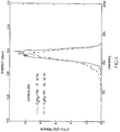
- Fig. 3 shows the Forward Recoil Detection (FRD) spectra of a He- and Ar-PECVD carbon film before annealing.
- Fig. 4 shows the FRD spectra of a He- and Ar-PECVD carbon film after annealing.
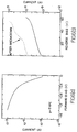
- Figs. 5(a) and (b) demonstrate the I-V characteristics of an amorphous carbon film/Si heterojunction, wherein Fig. 5(a) represents an n ⁇ and p ⁇ type Si heterojunction and Fig. 5(b) represents an n+ and p+ Si heterojunction.
- Figs. 6(a) and (b) demonstrate the I-V characteristics of a thin 32 nm amorphous carbon/Si (p ⁇ ) heterojunction wherein the reverse bias characteristics are shown (a) before and (b) after breakdown.
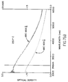
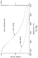
- Figs. 7(a) and (b) are two graphs showing the optical density vs. the wavelength for two quartz samples which were coated with a diamond-like carbon film by PECVD from acetylene/helium plasma wherein in Fig. 7(a) the dotted line (---) represents deposition at 250°C, and in Fig. 7(b) the solid line ( ⁇ ) represents deposition at room temperature (RT).
- Fig. 8 is a photograph showing the differences between patterning with (a) no ARC, (b) a spin on ARC, (c) an amorphous diamond-like carbon film ARC.
- the present invention relates to an improved method of producing extremely high quality hard amorphous diamond-like carbon films with the dielectric strength comparable to diamond by employing a low temperature plasma enhanced chemical vapor deposition from a hydrocarbon diluted in helium.
- the properties of the films produced by the present invention are vastly superior to those of plasma enhanced chemical vapor deposition films deposited from hydrocarbons which are either undiluted or diluted with other gases such as Ar, H2, etc.
- materials coated with the diamond-like carbon films of the present invention are extremely useful in a wide variety of applications.
- Fig. 1 is a diagram of a plasma enhanced chemical vapor deposition (PECVD) apparatus 8 that can be used to deposit the diamond-like carbon film of the present invention.
- the apparatus includes a reactor chamber 10 having a throttle valve 11 which separates the reactor chamber 10 from a vacuum pump not shown.
- a cathode 19 is mounted to the reactor chamber 10 and is isolated therefrom by a dielectric spacer 20.
- the cathode 19 is provided with a heater 17, an exhaust system 16 and sufficient means for allowing the inlet of N2 gas 18.
- a substrate 15 is secured to the inner end of the cathode 19.
- the cathode is electrically connected to a radio frequency source 14 which may be regulated and the impedance between the cathode 19 and the radio frequency source 14 is matched by utilizing a match box 13.
- the reactor chamber 10 also contains conduits 21 and 22 for introducing various materials into the reactor chamber 10.
- the pre-mixed hydrocarbon helium gas mixture is introduced into the reactor chamber 10 through conduit 21 while Ar gas for cleaning the substrate is introduced through conduit 22.
- the hydrocarbon gas which may be used in the present invention may be any hydrocarbon compound which is first capable of being gaseous and then able to form a plasma at the reaction condition employed by the present process.
- hydrocarbon implies that the molecules which make up the compound contains only carbon and hydrogen atoms.
- saturated or unsaturated hydrocarbon compounds may be employed by the present process.
- a saturated hydrocarbon compound is a compound whose molecules contain only carbon single bonds while an unsaturated compound is a compound whose molecules contain carbon double or triple bonds.
- Suitable hydrocarbons contemplated by the present process include alkanes, alkenes and alkynes.
- alkane is defined herein as a compound whose molecules contain only single bonds between carbon atoms.
- Suitable alkanes which may be employed by the present process include compounds such as methane, ethane, propane, butane and the like thereof. Of these alkanes, methane is most particularly preferred.
- Alkenes are defined herein as compounds whose molecules contain a carbon-carbon double bond.
- Alkene compounds which may be employed by the present process include compounds such as ethene, propene, n-butene and the like thereof.
- alkyne compound is defined herein as a hydrocarbon whose molecules contain a carbon-carbon triple bond.
- Suitable alkynes employed by the present process include acetylene, propylene, 1-butylene, 2-butylene and the like thereof. Of these alkynes, acetylene is most particularly preferred.
- the preferred hydrocarbon gas which is employed in forming the diamond-like carbon film is acetylene. Additionally, it should be recognized that mixtures of hydrocarbon gases such as acetylene/methane may also be contemplated as the hydrocarbon gas of the present invention.
- the hydrocarbon gas utilized in the instant invention is heavily diluted with helium.
- the term heavily diluted is defined herein as an admixture of a hydrocarbon with helium such that the final concentration of helium in the admixture constitutes from about 99 to about 50% of the gas mixture. More preferably, the hydrocarbon is diluted with helium such that the final concentration of hydrocarbon in the admixture is from about 2 to about 10%. Most preferably, the hydrocarbon constitutes about 2% of the overall gas mixture.
- Gases employed by the present invention have a purity greater than about 95.5%.
- the gases have a purity in the range from about 98.5 to about 99.99%.
- the gases have a purity greater than 99.99%.
- the high purity gases are pre-mixed in the same gas cylinder before being introduced in the reaction chamber.
- the gas mixture is introduced into the chamber by first passing it through a flow controller at a sufficient flow to provide a total pressure of hydrocarbon and helium from about 1 mTorr to about 600 mTorr.
- the pressure of hydrocarbon helium mixture be about 20-200 mTorr.
- the above conditions can also be obtained by introducing each gas separately through flow controllers providing the desired partial pressures.
- Suitable substrates which may be coated with the diamond-like film include materials such as plastics; metals; glass plates; magnetic heads; electronic chips; electronic circuit boards; semiconductor devices and the likes thereof.
- the substrate to be coated may be any shape or size provided that the substrate may be placed into the reaction chamber of the PECVD device. Thus, regular or irregular shape objects having any dimension may be used in the present invention.
- the substrate is mounted on a rf cathode inside the reaction chamber of the PECVD device.
- the reaction chamber is then tightly sealed and evacuated until a pressure reading in the range of about 1 x 10 ⁇ 4 to about 1 x 10 ⁇ 7 Torr is obtained.
- the substrate is then heated to a temperature from about 25 to 400°C.
- the substrate is heated to a temperature from about 200 to 300°C.
- the substrate is heated to a temperature of about 270°C prior to introducing the gas mixture into the reaction chamber.
- the temperature of the substrate is then held constant throughout the entire deposition process.
- the material may or may not be subjected to in-situ plasma cleaning prior to depositing the diamond-like carbon film.
- Suitable cleaning techniques employed by the present invention include H2, Ar, O2 and N2 plasma sputter etching techniques.
- the admixed gas is introduced into the reaction chamber at a flow of about 10 to about 100 sccm. More preferably, the flow rate of the reactant gas is from about 30 to about 80 sccm. Most preferably, the flow rate of the admixture of hydrocarbon and helium is about 50 sccm.
- the mixture is introduced into the reaction chamber at a pressure of about 1 to about 1000 m Torr. It is another preferred aspect of the instant invention that the admixture be introduced at a pressure of about 20 m Torr.
- the cathode bias was held fixed at a voltage from about -90 to about -300 V throughout the deposition process. Most preferably, the cathode bias was maintained at -100 V throughout the experiment. This voltage is supplied to the rf cathode by using an rf choke-isolated dc power supply source. To minimize damage to the substrate material during the deposition process a low rf power density should be utilized. Typically this involves applying an rf power density from about 3 to about 10 mW/cm2. More preferably, the rf power density employed by the present invention is maintained at 6 mW/cm2 throughout the deposition process.
- the diamond-like carbon film is deposited onto the substrate at a rate such that an essentially continuous coating of the film on the substrate is obtained. More specifically, by employing the previously mentioned operation parameters, the diamond-like carbon film is deposited onto the substrate at a rate of about 0.5 to 5 nm/min (about 5 to 50 ⁇ /min). The most preferred rate of depositing the diamond-like carbon film onto the substrate is at a rate of about 2 nm/min (about 20 ⁇ /min).
- the diamond-like carbon films deposited on the substrate are from about 10 to about 1000 nm (about 100 to about 10,000 ⁇ ) thick. More preferably, the thickness of the diamond-like carbon coating is from about 40 to about 200 nm (about 400 to about 2000 ⁇ ). It should be noted that by changing the resultant film thickness the optical density of the film can be changed. Thus, it is quite possible to tailor make a substrate with a defined optical density by merely increasing or decreasing the thickness of the film.
- the preferred optical densities of the diamond-like carbon films prepared by the present process are in the range from about 1 to about 3 at a wavelength of 248 nm which corresponds to a film thickness of about 100 to about 300 nm (about 1000 to about 3000 ⁇ ).
- the coated material depending on its application may or may not be annealed.
- Annealing typically involves heating the substrate in an atmosphere of Ar/H2 at 590°C for a time period of about 3 to about 5 hours.
- the diamond-like carbon film deposited in accordance with the process of the present invention are characterized as being amorphous, hard, thermally stable and optically transparent. Additionally, the diamond-like carbon films deposited by PECVD from a hydrocarbon/helium gas mixture have dielectric strength comparable to those normally associated with diamond films. The diamond-like carbon film deposited from a hydrocarbon/helium gas mixture in accordance with the present invention has a dielectric strength close to 10 MV/cm.
- the diamond-like carbon films of the present invention also provide a substrate with an extremely hard protective coating.
- the films deposited by the instant invention have a Young modulus of about 213 GPa to about 278 GPa which corresponds to a hardness of about 22.8 GPa to about 38.4 GPa.
- the film hardness is measured herein by using a nanoindenter from Nano Instruments, Knoxville, TN.
- the diamond-like carbon films of the present invention formed on the substrate are also optically transparent.
- the films are optically transparent at wavelengths of about 450 to about 750 nm, preferably about 550 to about 750 nm. Films which are optically transparent are suitable for use as coatings for plastic lenses or goggles.
- the diamond-like carbon films deposited by the instant invention are thermally stable at temperatures exceeding 590°C.
- This high thermal stability of the resultant diamond-like carbon films exceeds those values previously reported for PECVD using undiluted hydrocarbon or a hydrocarbon/Ar gas mixture.
- the improved thermal stability of the film obtained using a hydrocarbon/He gas mixture indicates that helium may play an important role in stabilizing the sp3 coordination of the carbon atoms in the resultant film.
- thermal stability in this instance appears to be due to the properties of plasma excited helium.
- the diamond-like carbon films of the present invention are exceptionally hard having the hereinabove defined Young's modulus and hardness, the film when applied to a plastic surface results in a coating that is highly scratch resistant and UV protective. Highly scratch resistant and UV inhibiting coatings are extremely important aspects which one must take into consideration when developing a coating for plastic lenses, goggles, car windows, etc.
- Fig. 2 is a cross-sectional diagram of a plastic lens coated with an amorphous diamond-like carbon film of the present invention produced by PECVD from an acetylene/helium plasma.
- the plastic lens is made from a polymethylmethacrylate (PMMA) material (1) which is soft and easy to scratch.
- PMMA polymethylmethacrylate
- the amorphous diamond-like carbon film (2) is deposited onto the surface of the plastic lens in accordance with the present invention, an improved scratch resistant coating is obtained.
- the plastic lens coated with the film of the instant invention provides improved UV protection over prior art films.
- the diamond-like carbon films act as a deep UV antireflective coating (ARC) which are needed to fabricate memory chips or other devices.
- ARC deep UV antireflective coating
- Such coatings effectively reduce the reflectivity effects when exposing and patterning a single layer deep UV resist used in circuit fabrication on memory chips.
- an ARC is made of polymers spun on the wafer, however, this results in poor process control because the ARC material reacts with the photoresist (PR) degrading the ARC/PR interface.
- spin-on ARC are not suitable for coating fine lithographic features such as 0.5 ⁇ m (wide) x > 1 ⁇ m (deep) trenches.
- the films formed by the present invention readily etch in oxygen plasma at a rate comparable to those of photoresists.
- the film when coated onto a memory chip may be easily removed by O2 plasma treatments typically used for photoresist residue removal without damaging the photoresist profile.
- the index of refraction of the films is similar to that reported for organic photoresist thus reflections at the ARC/photoresist interface are minimized as opposed to inorganic ARC of higher index.
- the diamond-like carbon films formed by the present invention may be used as an ideal absorber for deep UV photomasks. Such photomasks will be used as an alternative to chrome mask blanks which are commonly employed in the art. This process will eliminate all of the environmentally hazardous aspects of the chrome deposition, wet and RIE processes. Furthermore, the carbon masks containing the film of the present invention brings with it the high thermal conductivity of diamond as well as the hardness. Thus, these films can also be used as a direct patterned mask material and be ablated using a 193 nm laser in a reticle generation machine.
- the carbon photomask absorber having the film formed from an acetylene/helium plasma are etched at the same rate as photoresist in an oxygen plasma RIE thus eliminating the chrome wet etch and RIE process which produce toxic waste products thus, patterning the mask is a simpler and environmentally more acceptable process.
- the carbon films of the present invention have a reflectivity of 13.5% at 248 nm as compared to antireflecting chrome at 27%. This nearly 2X difference will serve to reduce the unwanted flare reflected from the reticle/mask.
- the carbon films as a photomask absorber can be deposited at a thickness of about 200 nm (about 2000 ⁇ ) which corresponds to an optical density of about 2.3.
- the films can also be used as an attenuated phase mask. In this application a film thickness of 120 nm (1200 ⁇ ) would be required for a ⁇ phase change.
- the following example is given to illustrate the process of depositing a diamond-like carbon films onto a substrate by plasma-enhanced chemical vapor deposition from a hydrocarbon/helium gas mixture.
- the Si substrates were then loaded on to the rf cathode of the PECVD device in Fig. 1. Thereafter, the system was evacuated to a partial pressure reading of about 1 x 10 ⁇ 6 Torr. The substrates were then heated to a temperature of about 250°C. Upon obtaining the desired substrate temperature the amorphous diamond-like carbon films were deposited from a mixture of acetylene/helium at a pressure of about 20 mTorr.
- the gases employed by the present process have a purity of greater than about 99.99% and furthermore the admixture gas comprise 98% acetylene and 2% helium.
- a rf power density of about 6 mW/cm2 was utilized in this experiment.
- the admixture gas was introduced into the reactor chamber at a flow of about 50 sccm.
- the rf plasma was ignited such that a negative cathode self-bias of -100V was maintained throughout the process.
- the diamond-like carbon was deposited onto the substrates at a rate of about 1.8 nm/min (about 18 ⁇ /min). The process was stopped after a film thickness of about 90 nm (about 900 ⁇ ) was obtained.
- the following comparative example illustrates the importance of utilizing an acetylene/helium gas mixture in providing a diamond-like carbon film with improved thermal stability.
- Diamond-like carbon films in this example were deposited in accordance with the procedure described in Example 1 however the admixture contained an acetylene/Ar (2% Ar) mixture.
- the hydrogen content is a key parameter in defining the film properties because the hardness of the film is attributed to the formation of sp3 bonds which contain at least 1,2 or even 3 hydrogen atoms.
- the poor thermal stability of PECVD amorphous films is attributed to H loss leading to the formation of dehydrogenated sp2 bonds (graphite) after thermal stress.
- the H content for the Ar- and He-PECVD process before and after thermal stress by forward recoil detection (FRD) were measured. This technique gives a direct measurement of the number of H atoms contained in the film.
- Fig. 3 shows the FRD spectra of He- and Ar-PECVD carbon films.
- the H content is 26 and 22 at. %, respectively. These numbers are measured by comparison to a known calibrated reference.
- Fig. 4 shows the same spectra after annealing at about 590°C for 3 hrs in Ar/H2 ambient. The H content decreased to 17 and 15 at. %, respectively.
- the Ar-PECVD film became hazy and soft. A roughening of the film may explain the peak asymmetry i.e. the tail, in the spectra of the annealed sample.
- the He-PECVD sample also lost H but the film was still hard (i.e., it could not be scratched by a razor blade).
- thermo stability of a PECVD amorphous carbon film can be greatly enhanced by diluting hydrocarbon gases in He rather than Ar.
- An amorphous carbon film deposited by PECVD of C2H2/He preserved its hardness after annealing at 590°C. This stability appears to be related to a better film nucleation which helps to stabilize the sp3 tetrahedral coordination, rather than to the H content.
- the following example illustrates the electrical properties on the diamond-like carbon films formed by PECVD from an acetylene/helium gas mixture.
- the two materials employed in this example comprise an Al/amorphous carbon/Cr and Al/amorphous carbon/Si.
- the amorphous diamond-like carbon film was deposited onto the Cr and Si substrate in accordance with the procedure of Example I.
- Figs. 5(a) and (b) The I-V characteristics of the coated Al/Si structure for four different Si doping concentrations are shown in Figs. 5(a) and (b) wherein Fig. 5(a) represents an n ⁇ and p ⁇ type Si heterojunction and Fig. 5(b) represents an n+ and p+ type Si heterojunction.
- the silicon doping was ⁇ 1015cm ⁇ 3 for n ⁇ and p ⁇ and 1019cm ⁇ 3 for n+ and p+.
- the I-V characteristics have a strong dependence on the Si substrate doping and therefore they can be attributed to the amorphous carbon/Si heterojunction and not to the metal/carbon interface.
- Fig. 5b shows the I-V curves at high Si doping.
- Fig. 5a shows that the barrier heights for the amorphous diamond-like carbon film to n- and p- type Si are different.
- the p- type material gives a barrier height 0.2 eV higher than n- type.
- This difference can be measured by comparing the reverse bias saturation currents for the n and p materials assuming that the current density is, J, J ⁇ exp(- ⁇ b /kT)x[exp(qV/kT)-1] where ⁇ b is the barrier at the junction, k is the Boltzmann constant, T is the temperature, q is the charge and V is the applied voltage.
- the band-edge Fermi level energy differences are also about the same.
- the optical bandgap from absorption measurements is 1.1 eV for the amorphous carbon film which roughly matches the Si bandgap of 1.12 eV (at room temperature). Therefore the 0.2 eV difference can be attributed to an offset between the amorphous carbon film and the Si energy band edge; specifically, the electron affinity of the amorphous carbon film is less than that of Si by a few tenths of an eV. This would explain the higher barrier observed for the p- type heterostructure when compared to the n- type.
- Figs. 6 (a) and (b) show the I-V characteristic for a heterojunction with a very thin 32 nm amorphous diamond-like carbon film.
- the silicon is p- type.
- breakdown occurs at 60V or 19 MV/cm. After breakdown the reverse leakage current increases by approximately two orders of magnitude. The same effect was observed for heterojunctions with a 100 nm film thickness. This implies that breakdown occurs at the junction rather than in the carbon film since no film thickness dependence was observed. Thus, only a very high junction breakdown was obtained under reverse bias. This indicates that the amorphous carbon film breakdown is also very close to the diamond breakdown of approximately 10 MV/cm.
- the following example illustrates one important application for the diamond-like carbon films formed by PECVD from acetylene/helium plasma. More specifically, the example shows that the diamond-like carbon films of the present invention may be successfully used as a protective coating for PMMA plastic lenses.
- Plastic lenses made for PMMA are usually soft and easy to scratch thus protective coating for the lenses is highly desirable.
- Scratch resistant coating which can also provide UV protection are available in the art however these coating are not hard enough and do not provide sufficient shielding form the brightness of the sun.
- the plastic lens was first cleaned with an isopropyl alcohol solution and then loaded into the reactor chamber. Thereafter, the lens was sputter cleaned in Ar at 600 V, 5m Torr, for 5 min. This sputter cleaning process was conducted to assure good adhesion of the diamond-like carbon film onto the lens.
- the PECVD carbon film was deposited in accordance with the procedure described in Example I, however, the temperature of the substrate was kept at 25°C to prevent high temperature deterioration of the lens properties.
- a film having a thickness of 90 nm was deposited.
- the resultant film is amber in color and provides UV protection and shielding from the sun brightness.
- the film provides improved scratch-resistant protection for the lens as determined by rubbing steel wool on it.
- Fig. 7 (a) and (b) show the optical densities as a function of wavelength for two carbon coatings on quartz deposited at room temperature. Both films are hard, have an amber color and are transparent in the visible region of the electromagnetic spectrum. Note that thicker coatings give higher UV protection with optical densities >2.
- the following example illustrates the use of the amorphous diamond-like carbon film as an anti-reflective coating (ARC) for memory chip fabrication.
- the diamond-like carbon film was deposited onto the memory chip in accordance with the process described in Example I.
- a memory chip containing no ARC and one containing a spin-on ARC coating were also prepared for comparison.
- Figs. 8(a)-8(c) illustrate the differences between patterning with (a) no ARC, (b) a spin-on ARC and (c) an amorphous diamond-like carbon film.
- an improvement in the patterning of the single layer resist is obtained.
- the photoresist profile is not damaged by using the films of the present invention.
- Fig. 8(c) wherein the photoresist edge profile represented by the verticle lines in the figure are more clearly defined than the photoresist edge profiles of either Figs. 8(a) or 8(b).
- the line width of the photoresist edge profile in Fig. 8(c) is 0.35 ⁇ m.
Landscapes
- Chemical & Material Sciences (AREA)
- Physics & Mathematics (AREA)
- General Physics & Mathematics (AREA)
- Optics & Photonics (AREA)
- Materials Engineering (AREA)
- Organic Chemistry (AREA)
- Chemical Kinetics & Catalysis (AREA)
- Engineering & Computer Science (AREA)
- Inorganic Chemistry (AREA)
- Mechanical Engineering (AREA)
- Metallurgy (AREA)
- General Chemical & Material Sciences (AREA)
- Chemical Vapour Deposition (AREA)
- Crystals, And After-Treatments Of Crystals (AREA)
- Formation Of Insulating Films (AREA)
- Preparing Plates And Mask In Photomechanical Process (AREA)
- Coating Of Shaped Articles Made Of Macromolecular Substances (AREA)
- Solid-Phase Diffusion Into Metallic Material Surfaces (AREA)
- Carbon And Carbon Compounds (AREA)
Applications Claiming Priority (2)
| Application Number | Priority Date | Filing Date | Title |
|---|---|---|---|
| US08/001,374 US5470661A (en) | 1993-01-07 | 1993-01-07 | Diamond-like carbon films from a hydrocarbon helium plasma |
| US1374 | 1995-07-24 |
Publications (2)
| Publication Number | Publication Date |
|---|---|
| EP0605814A1 true EP0605814A1 (fr) | 1994-07-13 |
| EP0605814B1 EP0605814B1 (fr) | 1996-09-04 |
Family
ID=21695724
Family Applications (1)
| Application Number | Title | Priority Date | Filing Date |
|---|---|---|---|
| EP93120065A Expired - Lifetime EP0605814B1 (fr) | 1993-01-07 | 1993-12-13 | Films de carbone diamantin fabriqués à l'aide d'un plasma à base d'hélium et d'hydrocarbure |
Country Status (4)
| Country | Link |
|---|---|
| US (2) | US5470661A (fr) |
| EP (1) | EP0605814B1 (fr) |
| JP (1) | JP2553310B2 (fr) |
| DE (1) | DE69304503T2 (fr) |
Cited By (18)
| Publication number | Priority date | Publication date | Assignee | Title |
|---|---|---|---|---|
| EP0743375A3 (fr) * | 1995-03-31 | 1997-05-21 | Ceramoptec Gmbh | Procédé de fabrication de revêtements de carbone semblable à du diamant |
| EP0734059A3 (fr) * | 1995-03-24 | 1997-08-13 | Shinko Electric Ind Co | Dispositif semi-conducteur à dimensions de puce et procédé de fabrication |
| DE19651953A1 (de) * | 1996-12-13 | 1998-07-02 | Bayer Bitterfeld Gmbh | Vorrichtung zum Verpressen von fließfähigen Feststoffen oder halbfesten Stoffen |
| WO1998058097A1 (fr) * | 1997-06-18 | 1998-12-23 | Northeastern University | Procede permettant de revetir des aretes de carbone de type diamant |
| EP0773167A4 (fr) * | 1994-08-11 | 1999-08-18 | Kirin Brewery | Recipients de plastique a revetement mince de carbone, leur appareil de fabrication et procede associe |
| EP1022614A4 (fr) * | 1998-07-31 | 2001-08-29 | Hoya Corp | Ebauche pour photomasque, photomasque, ses procedes de fabrication et procede de formage de micromodeles |
| FR2809190A1 (fr) * | 2000-05-22 | 2001-11-23 | Centre Nat Rech Scient | Procede de fabrication d'un modulateur de transmission pour microlithographie en ultraviolet profond et modulateur obtenu par ce procede |
| EP0949663A3 (fr) * | 1998-04-08 | 2002-11-13 | Nec Corporation | Dépôt d'une couche isolante comprenant du carbon |
| WO2003068502A1 (fr) * | 2002-02-13 | 2003-08-21 | Guardian Indusries Corp. | Procede de fabrication d'un bloc-fenetre |
| WO2003076184A1 (fr) * | 2002-03-07 | 2003-09-18 | Guardian Industries Corp. | Procede de fabrication d'un bloc-fenetre comprenant une couche de carbone sous forme de diamant amorphe (dlc) |
| RU2244983C1 (ru) * | 2003-07-14 | 2005-01-20 | Физический институт им. П.Н. Лебедева Российской академии наук | Способ получения алмазоподобных пленок для инкапсуляции солнечных фотоэлектрических элементов |
| US7060322B2 (en) | 2003-09-02 | 2006-06-13 | Guardian Industries Corp. | Method of making heat treatable coated article with diamond-like carbon (DLC) coating |
| US7443097B2 (en) | 2001-02-21 | 2008-10-28 | Semiconductor Energy Laboratory Co., Ltd. | Light emitting device and electronic equipment |
| EP1520421A4 (fr) * | 2002-07-09 | 2011-08-17 | Gentex Corp | Systeme de vision d'un vehicule a plage dynamique elevee |
| EP2105953A4 (fr) * | 2006-12-01 | 2011-12-14 | Tokyo Electron Ltd | Film de carbone amorphe, dispositif semi-conducteur, procédé de formation de film, appareil de formation de film et support de stockage |
| CN109637926A (zh) * | 2015-10-09 | 2019-04-16 | 应用材料公司 | 超高模量与蚀刻选择性的硼-碳硬掩模膜 |
| WO2022055732A1 (fr) * | 2020-09-08 | 2022-03-17 | Applied Materials, Inc. | Carbone amorphe pour élément de remplissage d'espace |
| JP2023538528A (ja) * | 2020-08-07 | 2023-09-08 | アプライド マテリアルズ インコーポレイテッド | 低応力炭素含有層の堆積 |
Families Citing this family (190)
| Publication number | Priority date | Publication date | Assignee | Title |
|---|---|---|---|---|
| US6255718B1 (en) | 1995-02-28 | 2001-07-03 | Chip Express Corporation | Laser ablateable material |
| IL112826A (en) * | 1995-02-28 | 1998-09-24 | Chip Express Israel Ltd | Method for depositing a plasma deposited polymer |
| JP3176558B2 (ja) * | 1996-02-09 | 2001-06-18 | 麒麟麦酒株式会社 | コーティングフィルムおよびその製造方法 |
| US5840427A (en) * | 1996-05-21 | 1998-11-24 | Teledyne Industries Incorporated | Method for making corrosion resistant electrical components |
| US5858477A (en) | 1996-12-10 | 1999-01-12 | Akashic Memories Corporation | Method for producing recording media having protective overcoats of highly tetrahedral amorphous carbon |
| EP0848083A3 (fr) * | 1996-12-12 | 2001-03-07 | Eastman Kodak Company | Revêtements protecteurs inorganique ou en i-carbone et méthode à température ambiante pour leur fabrication |
| US5879775A (en) * | 1996-12-12 | 1999-03-09 | Eastman Kodak Compnay | Protective inorganic and DLC coatings for plastic media such as plastic cards |
| US6428894B1 (en) * | 1997-06-04 | 2002-08-06 | International Business Machines Corporation | Tunable and removable plasma deposited antireflective coatings |
| US6030904A (en) * | 1997-08-21 | 2000-02-29 | International Business Machines Corporation | Stabilization of low-k carbon-based dielectrics |
| US5981000A (en) * | 1997-10-14 | 1999-11-09 | International Business Machines Corporation | Method for fabricating a thermally stable diamond-like carbon film |
| US6103305A (en) * | 1997-11-26 | 2000-08-15 | Sandia Corporation | Method of forming a stress relieved amorphous tetrahedrally-coordinated carbon film |
| US6726993B2 (en) * | 1997-12-02 | 2004-04-27 | Teer Coatings Limited | Carbon coatings, method and apparatus for applying them, and articles bearing such coatings |
| US6448655B1 (en) * | 1998-04-28 | 2002-09-10 | International Business Machines Corporation | Stabilization of fluorine-containing low-k dielectrics in a metal/insulator wiring structure by ultraviolet irradiation |
| US7378146B1 (en) * | 1998-08-05 | 2008-05-27 | International Business Machines Corporation | Transparent hard coats for optical elements |
| US6265779B1 (en) | 1998-08-11 | 2001-07-24 | International Business Machines Corporation | Method and material for integration of fuorine-containing low-k dielectrics |
| JP2000164565A (ja) * | 1998-11-26 | 2000-06-16 | Sony Corp | 半導体製造装置 |
| CH697036A5 (de) * | 1998-12-02 | 2008-03-31 | Sulzer Metco Ag | Verfahren zur Plasma-Oberflächenbehandlung von Substraten sowie Einrichtung zur Durchführung des Verfahrens. |
| US6964731B1 (en) | 1998-12-21 | 2005-11-15 | Cardinal Cg Company | Soil-resistant coating for glass surfaces |
| US6660365B1 (en) | 1998-12-21 | 2003-12-09 | Cardinal Cg Company | Soil-resistant coating for glass surfaces |
| US6974629B1 (en) | 1999-08-06 | 2005-12-13 | Cardinal Cg Company | Low-emissivity, soil-resistant coating for glass surfaces |
| US6528865B1 (en) | 1999-01-22 | 2003-03-04 | Intel Corporation | Thin amorphous fluorocarbon films |
| KR100307629B1 (ko) | 1999-04-30 | 2001-09-26 | 윤종용 | 하이드로 카본계의 가스를 이용한 반사방지막의 형성 및 적용방법 |
| US6447891B1 (en) | 1999-05-03 | 2002-09-10 | Guardian Industries Corp. | Low-E coating system including protective DLC |
| US6335086B1 (en) | 1999-05-03 | 2002-01-01 | Guardian Industries Corporation | Hydrophobic coating including DLC on substrate |
| US6312808B1 (en) | 1999-05-03 | 2001-11-06 | Guardian Industries Corporation | Hydrophobic coating with DLC & FAS on substrate |
| US6273488B1 (en) | 1999-05-03 | 2001-08-14 | Guardian Industries Corporation | System and method for removing liquid from rear window of a vehicle |
| US6461731B1 (en) | 1999-05-03 | 2002-10-08 | Guardian Industries Corp. | Solar management coating system including protective DLC |
| US6280834B1 (en) | 1999-05-03 | 2001-08-28 | Guardian Industries Corporation | Hydrophobic coating including DLC and/or FAS on substrate |
| US6277480B1 (en) * | 1999-05-03 | 2001-08-21 | Guardian Industries Corporation | Coated article including a DLC inclusive layer(s) and a layer(s) deposited using siloxane gas, and corresponding method |
| US6338901B1 (en) | 1999-05-03 | 2002-01-15 | Guardian Industries Corporation | Hydrophobic coating including DLC on substrate |
| US6261693B1 (en) | 1999-05-03 | 2001-07-17 | Guardian Industries Corporation | Highly tetrahedral amorphous carbon coating on glass |
| US6423384B1 (en) | 1999-06-25 | 2002-07-23 | Applied Materials, Inc. | HDP-CVD deposition of low dielectric constant amorphous carbon film |
| KR100304708B1 (ko) * | 1999-07-14 | 2001-11-01 | 윤종용 | 이중층 반사방지막을 갖는 반도체소자 및 그 제조방법 |
| US6579833B1 (en) | 1999-09-01 | 2003-06-17 | The Board Of Trustees Of The University Of Illinois | Process for converting a metal carbide to carbon by etching in halogens |
| US20040028906A1 (en) * | 2000-01-04 | 2004-02-12 | Anderson Jerrel Charles | Diamond-like carbon coating on glass and plastic for added hardness and abrasion resistance |
| JP5121090B2 (ja) * | 2000-02-17 | 2013-01-16 | アプライド マテリアルズ インコーポレイテッド | アモルファスカーボン層の堆積方法 |
| US6573030B1 (en) * | 2000-02-17 | 2003-06-03 | Applied Materials, Inc. | Method for depositing an amorphous carbon layer |
| US6713179B2 (en) | 2000-05-24 | 2004-03-30 | Guardian Industries Corp. | Hydrophilic DLC on substrate with UV exposure |
| JP2002194547A (ja) * | 2000-06-08 | 2002-07-10 | Applied Materials Inc | アモルファスカーボン層の堆積方法 |
| FR2812665B1 (fr) * | 2000-08-01 | 2003-08-08 | Sidel Sa | Procede de depot de revetement par plasma, dispositif de mise en oeuvre du procede et revetement obtenu par un tel procede |
| US6346183B1 (en) | 2000-08-03 | 2002-02-12 | International Business Machines Corporation | Use of thin carbon films as a bottom anti-reflective coating in manufacturing magnetic heads |
| US6524755B2 (en) | 2000-09-07 | 2003-02-25 | Gray Scale Technologies, Inc. | Phase-shift masks and methods of fabrication |
| US6368924B1 (en) * | 2000-10-31 | 2002-04-09 | Motorola, Inc. | Amorphous carbon layer for improved adhesion of photoresist and method of fabrication |
| US6610360B2 (en) * | 2001-11-28 | 2003-08-26 | Guardian Industries Corp. | Buffing diamond-like carbon (DLC) to improve scratch resistance |
| EP1321545A1 (fr) * | 2001-12-20 | 2003-06-25 | Max-Planck-Gesellschaft zur Förderung der Wissenschaften e.V. | Procédé pour la préparation des particules avec la structure de diamant |
| US6783253B2 (en) | 2002-03-21 | 2004-08-31 | Guardian Industries Corp. | First surface mirror with DLC coating |
| US6541397B1 (en) * | 2002-03-29 | 2003-04-01 | Applied Materials, Inc. | Removable amorphous carbon CMP stop |
| US6919536B2 (en) | 2002-04-05 | 2005-07-19 | Guardian Industries Corp. | Vehicle window with ice removal structure thereon |
| US6903023B2 (en) * | 2002-09-16 | 2005-06-07 | International Business Machines Corporation | In-situ plasma etch for TERA hard mask materials |
| US7224532B2 (en) * | 2002-12-06 | 2007-05-29 | Chevron U.S.A. Inc. | Optical uses diamondoid-containing materials |
| US6904935B2 (en) | 2002-12-18 | 2005-06-14 | Masco Corporation Of Indiana | Valve component with multiple surface layers |
| US7866343B2 (en) | 2002-12-18 | 2011-01-11 | Masco Corporation Of Indiana | Faucet |
| US8555921B2 (en) | 2002-12-18 | 2013-10-15 | Vapor Technologies Inc. | Faucet component with coating |
| US7866342B2 (en) | 2002-12-18 | 2011-01-11 | Vapor Technologies, Inc. | Valve component for faucet |
| US8220489B2 (en) | 2002-12-18 | 2012-07-17 | Vapor Technologies Inc. | Faucet with wear-resistant valve component |
| US20040157430A1 (en) * | 2003-02-07 | 2004-08-12 | Asml Netherlands B.V. | Methods and apparatus for processing semiconductor wafers with plasma processing chambers in a wafer track environment |
| US7052585B2 (en) * | 2003-03-11 | 2006-05-30 | Guardian Industries Corp. | Coated article including titanium oxycarbide and method of making same |
| US7306778B2 (en) * | 2003-06-19 | 2007-12-11 | Nanotech Llc | Diamond films and methods of making diamond films |
| DE10329535B4 (de) * | 2003-06-30 | 2007-02-22 | Sls Micro Technology Gmbh | Miniaturisierte Anreicherungsvorrichtung |
| US7129180B2 (en) * | 2003-09-12 | 2006-10-31 | Micron Technology, Inc. | Masking structure having multiple layers including an amorphous carbon layer |
| US7132201B2 (en) * | 2003-09-12 | 2006-11-07 | Micron Technology, Inc. | Transparent amorphous carbon structure in semiconductor devices |
| WO2005036627A1 (fr) * | 2003-10-03 | 2005-04-21 | Applied Materials, Inc. | Couche absorbante pour traitement de recuit de surface dynamique |
| US7109087B2 (en) * | 2003-10-03 | 2006-09-19 | Applied Materials, Inc. | Absorber layer for DSA processing |
| US7294404B2 (en) | 2003-12-22 | 2007-11-13 | Cardinal Cg Company | Graded photocatalytic coatings |
| DE102004002908B4 (de) * | 2004-01-20 | 2008-01-24 | Infineon Technologies Ag | Verfahren zum Herstellen eines Halbleiterbauelements oder einer mikromechanischen Struktur |
| US7464581B2 (en) * | 2004-03-29 | 2008-12-16 | Tokyo Electron Limited | Vacuum apparatus including a particle monitoring unit, particle monitoring method and program, and window member for use in the particle monitoring |
| ATE377580T1 (de) | 2004-07-12 | 2007-11-15 | Cardinal Cg Co | Wartungsarme beschichtungen |
| US7470633B2 (en) * | 2004-08-09 | 2008-12-30 | Asm Japan K.K. | Method of forming a carbon polymer film using plasma CVD |
| US7504344B2 (en) * | 2004-08-09 | 2009-03-17 | Asm Japan K.K. | Method of forming a carbon polymer film using plasma CVD |
| US7151040B2 (en) * | 2004-08-31 | 2006-12-19 | Micron Technology, Inc. | Methods for increasing photo alignment margins |
| US7910288B2 (en) | 2004-09-01 | 2011-03-22 | Micron Technology, Inc. | Mask material conversion |
| US7115525B2 (en) * | 2004-09-02 | 2006-10-03 | Micron Technology, Inc. | Method for integrated circuit fabrication using pitch multiplication |
| US7655387B2 (en) | 2004-09-02 | 2010-02-02 | Micron Technology, Inc. | Method to align mask patterns |
| US7923114B2 (en) | 2004-12-03 | 2011-04-12 | Cardinal Cg Company | Hydrophilic coatings, methods for depositing hydrophilic coatings, and improved deposition technology for thin films |
| US8092660B2 (en) | 2004-12-03 | 2012-01-10 | Cardinal Cg Company | Methods and equipment for depositing hydrophilic coatings, and deposition technologies for thin films |
| US7667277B2 (en) * | 2005-01-13 | 2010-02-23 | International Business Machines Corporation | TiC as a thermally stable p-metal carbide on high k SiO2 gate stacks |
| US7253118B2 (en) | 2005-03-15 | 2007-08-07 | Micron Technology, Inc. | Pitch reduced patterns relative to photolithography features |
| US7390746B2 (en) | 2005-03-15 | 2008-06-24 | Micron Technology, Inc. | Multiple deposition for integration of spacers in pitch multiplication process |
| US7611944B2 (en) | 2005-03-28 | 2009-11-03 | Micron Technology, Inc. | Integrated circuit fabrication |
| US7429536B2 (en) | 2005-05-23 | 2008-09-30 | Micron Technology, Inc. | Methods for forming arrays of small, closely spaced features |
| JP2006332357A (ja) * | 2005-05-26 | 2006-12-07 | Denso Corp | 炭化珪素半導体素子の製造方法 |
| US7560390B2 (en) | 2005-06-02 | 2009-07-14 | Micron Technology, Inc. | Multiple spacer steps for pitch multiplication |
| US7396781B2 (en) | 2005-06-09 | 2008-07-08 | Micron Technology, Inc. | Method and apparatus for adjusting feature size and position |
| JP4853857B2 (ja) | 2005-06-15 | 2012-01-11 | 東京エレクトロン株式会社 | 基板の処理方法,コンピュータ読み取り可能な記録媒体及び基板処理装置 |
| US8193642B2 (en) * | 2005-06-20 | 2012-06-05 | Tohoku University | Interlayer insulating film, interconnection structure, and methods of manufacturing the same |
| US7413981B2 (en) | 2005-07-29 | 2008-08-19 | Micron Technology, Inc. | Pitch doubled circuit layout |
| US20070026205A1 (en) | 2005-08-01 | 2007-02-01 | Vapor Technologies Inc. | Article having patterned decorative coating |
| US8123968B2 (en) | 2005-08-25 | 2012-02-28 | Round Rock Research, Llc | Multiple deposition for integration of spacers in pitch multiplication process |
| US7816262B2 (en) | 2005-08-30 | 2010-10-19 | Micron Technology, Inc. | Method and algorithm for random half pitched interconnect layout with constant spacing |
| US7829262B2 (en) * | 2005-08-31 | 2010-11-09 | Micron Technology, Inc. | Method of forming pitch multipled contacts |
| US7776744B2 (en) | 2005-09-01 | 2010-08-17 | Micron Technology, Inc. | Pitch multiplication spacers and methods of forming the same |
| US7759197B2 (en) | 2005-09-01 | 2010-07-20 | Micron Technology, Inc. | Method of forming isolated features using pitch multiplication |
| US7572572B2 (en) | 2005-09-01 | 2009-08-11 | Micron Technology, Inc. | Methods for forming arrays of small, closely spaced features |
| US7393789B2 (en) | 2005-09-01 | 2008-07-01 | Micron Technology, Inc. | Protective coating for planarization |
| US7657143B2 (en) * | 2005-10-07 | 2010-02-02 | Novatronix Corporation | Method for improving refractive index control in PECVD deposited a-SiNy films |
| US8664124B2 (en) | 2005-10-31 | 2014-03-04 | Novellus Systems, Inc. | Method for etching organic hardmasks |
| US8110493B1 (en) | 2005-12-23 | 2012-02-07 | Novellus Systems, Inc. | Pulsed PECVD method for modulating hydrogen content in hard mask |
| US7476933B2 (en) | 2006-03-02 | 2009-01-13 | Micron Technology, Inc. | Vertical gated access transistor |
| US7842558B2 (en) | 2006-03-02 | 2010-11-30 | Micron Technology, Inc. | Masking process for simultaneously patterning separate regions |
| US7410915B2 (en) * | 2006-03-23 | 2008-08-12 | Asm Japan K.K. | Method of forming carbon polymer film using plasma CVD |
| US7902074B2 (en) | 2006-04-07 | 2011-03-08 | Micron Technology, Inc. | Simplified pitch doubling process flow |
| JP2009534563A (ja) | 2006-04-19 | 2009-09-24 | 日本板硝子株式会社 | 同等の単独の表面反射率を有する対向機能コーティング |
| US8003310B2 (en) | 2006-04-24 | 2011-08-23 | Micron Technology, Inc. | Masking techniques and templates for dense semiconductor fabrication |
| US7488685B2 (en) | 2006-04-25 | 2009-02-10 | Micron Technology, Inc. | Process for improving critical dimension uniformity of integrated circuit arrays |
| US7846492B2 (en) | 2006-04-27 | 2010-12-07 | Guardian Industries Corp. | Photocatalytic window and method of making same |
| US7892662B2 (en) | 2006-04-27 | 2011-02-22 | Guardian Industries Corp. | Window with anti-bacterial and/or anti-fungal feature and method of making same |
| JP5176337B2 (ja) * | 2006-05-12 | 2013-04-03 | 株式会社デンソー | 皮膜構造及びその形成方法 |
| US20070269646A1 (en) * | 2006-05-18 | 2007-11-22 | Haverty Michael G | Bond termination of pores in a porous diamond dielectric material |
| US7795149B2 (en) | 2006-06-01 | 2010-09-14 | Micron Technology, Inc. | Masking techniques and contact imprint reticles for dense semiconductor fabrication |
| US7723009B2 (en) | 2006-06-02 | 2010-05-25 | Micron Technology, Inc. | Topography based patterning |
| US7981810B1 (en) | 2006-06-08 | 2011-07-19 | Novellus Systems, Inc. | Methods of depositing highly selective transparent ashable hardmask films |
| US20080011599A1 (en) | 2006-07-12 | 2008-01-17 | Brabender Dennis M | Sputtering apparatus including novel target mounting and/or control |
| US7611980B2 (en) | 2006-08-30 | 2009-11-03 | Micron Technology, Inc. | Single spacer process for multiplying pitch by a factor greater than two and related intermediate IC structures |
| US7666578B2 (en) | 2006-09-14 | 2010-02-23 | Micron Technology, Inc. | Efficient pitch multiplication process |
| KR101414420B1 (ko) * | 2006-11-22 | 2014-07-01 | 엔테그리스, 아이엔씨. | 기재 하우징의 다이아몬드형 탄소 코팅 |
| US7833574B2 (en) * | 2007-01-29 | 2010-11-16 | Guardian Industries Corp. | Method of making heat treated coated article using diamond-like carbon (DLC) coating and protective film |
| US20120015195A1 (en) | 2007-01-29 | 2012-01-19 | Guardian Industries Corp. and C.R.V.C. | Method of making heat treated and ion-beam etched/milled coated article using diamond-like carbon (dlc) coating and protective film |
| US8132426B2 (en) * | 2007-01-29 | 2012-03-13 | Guardian Industries Corp. | Method of making heat treated coated article using diamond-like carbon (DLC) coating and protective film |
| US8003167B2 (en) * | 2007-01-29 | 2011-08-23 | Guardian Industries Corp. | Method of making heat treated coated article using diamond-like carbon (DLC) coating and protective film |
| US20120040160A1 (en) | 2007-01-29 | 2012-02-16 | Guardian Industries Corp. | Method of making heat treated and ion-beam etched/milled coated article using diamond-like carbon (dlc) protective film |
| US8071166B2 (en) | 2007-01-29 | 2011-12-06 | Guardian Industries Corp. | Method of making heat treated coated article using diamond-like carbon (DLC) coating and protective film |
| US20120015196A1 (en) | 2007-01-29 | 2012-01-19 | Guardian Industries Corp. | Method of making heat treated coated article using diamond-like carbon (dlc) coating and protective film on acid-etched surface |
| US7914857B2 (en) * | 2007-01-29 | 2011-03-29 | Guardian Industries Corp. | Method of making heat treated coated article using diamond-like carbon (DLC) coating and protective film with oxygen content of protective film based on bending characteristics of coated article |
| US7981777B1 (en) | 2007-02-22 | 2011-07-19 | Novellus Systems, Inc. | Methods of depositing stable and hermetic ashable hardmask films |
| US7915166B1 (en) | 2007-02-22 | 2011-03-29 | Novellus Systems, Inc. | Diffusion barrier and etch stop films |
| JP2008215940A (ja) * | 2007-03-01 | 2008-09-18 | Canon Inc | 異物検査装置及びこれを用いた異物検査方法 |
| US7923373B2 (en) | 2007-06-04 | 2011-04-12 | Micron Technology, Inc. | Pitch multiplication using self-assembling materials |
| US8105660B2 (en) * | 2007-06-28 | 2012-01-31 | Andrew W Tudhope | Method for producing diamond-like carbon coatings using PECVD and diamondoid precursors on internal surfaces of a hollow component |
| US20090029067A1 (en) * | 2007-06-28 | 2009-01-29 | Sciamanna Steven F | Method for producing amorphous carbon coatings on external surfaces using diamondoid precursors |
| US8563229B2 (en) | 2007-07-31 | 2013-10-22 | Micron Technology, Inc. | Process of semiconductor fabrication with mask overlay on pitch multiplied features and associated structures |
| US8962101B2 (en) | 2007-08-31 | 2015-02-24 | Novellus Systems, Inc. | Methods and apparatus for plasma-based deposition |
| US7638441B2 (en) * | 2007-09-11 | 2009-12-29 | Asm Japan K.K. | Method of forming a carbon polymer film using plasma CVD |
| CA2664369A1 (fr) | 2007-09-14 | 2009-03-19 | Cardinal Cg Company | Revetements a faible entretien et procedes de production de revetements a faible entretien |
| US20090090382A1 (en) * | 2007-10-05 | 2009-04-09 | Asm Japan K.K. | Method of self-cleaning of carbon-based film |
| EP2052609A1 (fr) | 2007-10-24 | 2009-04-29 | Bayer CropScience AG | Combinaison d'herbicide |
| US7737039B2 (en) | 2007-11-01 | 2010-06-15 | Micron Technology, Inc. | Spacer process for on pitch contacts and related structures |
| US7659208B2 (en) | 2007-12-06 | 2010-02-09 | Micron Technology, Inc | Method for forming high density patterns |
| US7790531B2 (en) | 2007-12-18 | 2010-09-07 | Micron Technology, Inc. | Methods for isolating portions of a loop of pitch-multiplied material and related structures |
| US7993462B2 (en) | 2008-03-19 | 2011-08-09 | Asm Japan K.K. | Substrate-supporting device having continuous concavity |
| US8030218B2 (en) | 2008-03-21 | 2011-10-04 | Micron Technology, Inc. | Method for selectively modifying spacing between pitch multiplied structures |
| US20090246399A1 (en) * | 2008-03-28 | 2009-10-01 | Asm Japan K.K. | Method for activating reactive oxygen species for cleaning carbon-based film deposition |
| US8467224B2 (en) * | 2008-04-11 | 2013-06-18 | Sandisk 3D Llc | Damascene integration methods for graphitic films in three-dimensional memories and memories formed therefrom |
| US7632549B2 (en) * | 2008-05-05 | 2009-12-15 | Asm Japan K.K. | Method of forming a high transparent carbon film |
| US20090297731A1 (en) * | 2008-05-30 | 2009-12-03 | Asm Japan K.K. | Apparatus and method for improving production throughput in cvd chamber |
| US7820556B2 (en) * | 2008-06-04 | 2010-10-26 | Novellus Systems, Inc. | Method for purifying acetylene gas for use in semiconductor processes |
| US7998881B1 (en) | 2008-06-06 | 2011-08-16 | Novellus Systems, Inc. | Method for making high stress boron-doped carbon films |
| US7906817B1 (en) | 2008-06-06 | 2011-03-15 | Novellus Systems, Inc. | High compressive stress carbon liners for MOS devices |
| US8435608B1 (en) | 2008-06-27 | 2013-05-07 | Novellus Systems, Inc. | Methods of depositing smooth and conformal ashable hard mask films |
| US8076208B2 (en) | 2008-07-03 | 2011-12-13 | Micron Technology, Inc. | Method for forming transistor with high breakdown voltage using pitch multiplication technique |
| WO2010009364A1 (fr) * | 2008-07-18 | 2010-01-21 | Sandisk 3D, Llc | Matériaux de commutation de résistivité à base de carbone et procédés de formage de ceux-ci |
| US8187671B2 (en) * | 2008-07-28 | 2012-05-29 | Centre Luxembourgeois De Recherches Pour Le Verre Et La Ceramique S.A. (C.R.V.C.) | Method of making heat treated coated article using diamond-like carbon (DLC) coating and protective film including removal of protective film via blasting |
| DE102008037621A1 (de) | 2008-08-14 | 2010-02-18 | Bayer Cropscience Ag | Herbizid-Kombination mit Dimethoxytriazinyl-substituierten Difluormethansulfonylaniliden |
| US8101497B2 (en) | 2008-09-11 | 2012-01-24 | Micron Technology, Inc. | Self-aligned trench formation |
| US8133555B2 (en) * | 2008-10-14 | 2012-03-13 | Asm Japan K.K. | Method for forming metal film by ALD using beta-diketone metal complex |
| US20100104770A1 (en) * | 2008-10-27 | 2010-04-29 | Asm Japan K.K. | Two-step formation of hydrocarbon-based polymer film |
| US8492282B2 (en) | 2008-11-24 | 2013-07-23 | Micron Technology, Inc. | Methods of forming a masking pattern for integrated circuits |
| CN101736313B (zh) * | 2008-11-26 | 2011-07-06 | 北京有色金属研究总院 | 一种在锗基片上制备类金刚石膜的方法 |
| US7955990B2 (en) * | 2008-12-12 | 2011-06-07 | Novellus Systems, Inc. | Method for improved thickness repeatability of PECVD deposited carbon films |
| FR2943660B1 (fr) * | 2009-03-25 | 2011-04-29 | Commissariat Energie Atomique | Procede d'elaboration de graphene |
| JP4990959B2 (ja) * | 2009-12-14 | 2012-08-01 | トーカロ株式会社 | 厚膜dlc被覆部材およびその製造方法 |
| US8288292B2 (en) | 2010-03-30 | 2012-10-16 | Novellus Systems, Inc. | Depositing conformal boron nitride film by CVD without plasma |
| US8563414B1 (en) | 2010-04-23 | 2013-10-22 | Novellus Systems, Inc. | Methods for forming conductive carbon films by PECVD |
| US8778295B2 (en) | 2010-08-11 | 2014-07-15 | Daniel Hodes | Combinatorial synthesis of diamond |
| US9061917B2 (en) | 2010-08-11 | 2015-06-23 | Unit Cell Diamond Llc | Combinatorial synthesis of the diamond unit cell |
| US10258959B2 (en) | 2010-08-11 | 2019-04-16 | Unit Cell Diamond Llc | Methods of producing heterodiamond and apparatus therefor |
| US9783885B2 (en) | 2010-08-11 | 2017-10-10 | Unit Cell Diamond Llc | Methods for producing diamond mass and apparatus therefor |
| US20120145676A1 (en) * | 2010-12-01 | 2012-06-14 | University Of North Texas | Metal Ablation in Supersonic Expansion Gas Coupled to an Ion Mass Filter |
| JP5904537B2 (ja) * | 2011-04-20 | 2016-04-13 | Ntn株式会社 | 非晶質炭素膜の成膜方法 |
| US9255029B2 (en) | 2012-04-17 | 2016-02-09 | Guardian Industries Corp. | Method of making heat treated coated article using TCO and removable protective film |
| SG195494A1 (en) | 2012-05-18 | 2013-12-30 | Novellus Systems Inc | Carbon deposition-etch-ash gap fill process |
| US9038419B2 (en) | 2012-06-08 | 2015-05-26 | Centre Luxembourgeois De Recherches Pour Le Verre Et La Ceramique S.A. (C.R.V.C.) | Method of making heat treated coated article using carbon based coating and protective film |
| US9514932B2 (en) | 2012-08-08 | 2016-12-06 | Applied Materials, Inc. | Flowable carbon for semiconductor processing |
| US9434640B2 (en) | 2012-12-04 | 2016-09-06 | Guardian Industries Corp. | Method of making heat treated coated article with carbon based coating and protective film |
| US9362133B2 (en) | 2012-12-14 | 2016-06-07 | Lam Research Corporation | Method for forming a mask by etching conformal film on patterned ashable hardmask |
| US9751800B2 (en) | 2013-02-06 | 2017-09-05 | Guardian Glass, LLC | Heat treatable coated article with tungsten-doped zirconium based layer(s) in coating |
| US9304396B2 (en) | 2013-02-25 | 2016-04-05 | Lam Research Corporation | PECVD films for EUV lithography |
| US9320387B2 (en) | 2013-09-30 | 2016-04-26 | Lam Research Corporation | Sulfur doped carbon hard masks |
| US9589799B2 (en) | 2013-09-30 | 2017-03-07 | Lam Research Corporation | High selectivity and low stress carbon hardmask by pulsed low frequency RF power |
| CN107111005A (zh) * | 2014-10-30 | 2017-08-29 | 住友电气工业株式会社 | 透镜和光学部件 |
| US10611678B2 (en) | 2016-11-04 | 2020-04-07 | Guardian Glass, LLC | Heat treatable coated article with carbon-doped zirconium based layer(s) in coating |
| US10604442B2 (en) | 2016-11-17 | 2020-03-31 | Cardinal Cg Company | Static-dissipative coating technology |
| WO2018226370A1 (fr) * | 2017-06-08 | 2018-12-13 | Applied Materials, Inc. | Films de carbone à basse température haute densité pour masque dur et autres applications de formation de motifs |
| US10611679B2 (en) | 2017-10-26 | 2020-04-07 | Guardian Glass, LLC | Coated article including noble metal and polymeric hydrogenated diamond like carbon composite material having antibacterial and photocatalytic properties, and/or methods of making the same |
| US20190127272A1 (en) | 2017-10-26 | 2019-05-02 | Guardian Glass, LLC | Coated article including noble metal and polymeric hydrogenated diamond like carbon composite material having antibacterial and photocatalytic properties, and/or methods of making the same |
| US10705273B2 (en) * | 2018-03-26 | 2020-07-07 | Raytheon Company | Multispectral interference coating with diamond-like carbon (DLC) film |
| US11469097B2 (en) | 2018-04-09 | 2022-10-11 | Applied Materials, Inc. | Carbon hard masks for patterning applications and methods related thereto |
| US11145509B2 (en) | 2019-05-24 | 2021-10-12 | Applied Materials, Inc. | Method for forming and patterning a layer and/or substrate |
| WO2020243342A1 (fr) | 2019-05-29 | 2020-12-03 | Lam Research Corporation | Masques durs en carbone sous forme de diamant amorphe à haute sélectivité, à faible contrainte et à faible teneur en hydrogène par rf basse fréquence pulsée à haute puissance |
| CN114342043A (zh) | 2019-08-30 | 2022-04-12 | 朗姆研究公司 | 低压下的高密度、模量和硬度的非晶碳膜 |
| DE102021200747A1 (de) | 2021-01-28 | 2022-07-28 | Carl Zeiss Smt Gmbh | Verfahren zum Bilden einer Schicht, optisches Element und optisches System |
Citations (4)
| Publication number | Priority date | Publication date | Assignee | Title |
|---|---|---|---|---|
| EP0157212A2 (fr) * | 1984-04-02 | 1985-10-09 | American Cyanamid Company | Article revêtu avec un film adhérent de carbone semblable à du diamant |
| WO1986000093A1 (fr) * | 1984-06-12 | 1986-01-03 | Battelle-Institut E.V. | Procede de fabrication de couches de carbone diamantines |
| EP0175980A2 (fr) * | 1984-09-10 | 1986-04-02 | Ovonic Synthetic Materials Company, Inc. | Procédé de dépôt d'un revêtement de carbone sur un substrat à l'aide d'une décharge luminescente et revêtements obtenus par ce procédé |
| EP0411435A1 (fr) * | 1989-07-31 | 1991-02-06 | Matsushita Electric Industrial Co., Ltd. | Appareillage por synthétiser un film mince de i-carbone |
Family Cites Families (15)
| Publication number | Priority date | Publication date | Assignee | Title |
|---|---|---|---|---|
| US4486286A (en) * | 1982-09-28 | 1984-12-04 | Nerken Research Corp. | Method of depositing a carbon film on a substrate and products obtained thereby |
| US4783361A (en) * | 1984-09-10 | 1988-11-08 | Ovonic Synthetic Materials Company, Inc. | Coated lenses |
| JPS61210518A (ja) * | 1985-03-13 | 1986-09-18 | Matsushita Electric Ind Co Ltd | 磁気記録媒体の製造方法 |
| US4603082A (en) * | 1985-04-29 | 1986-07-29 | Rca Corporation | Diamond-like film |
| EP0221531A3 (fr) * | 1985-11-06 | 1992-02-19 | Kanegafuchi Kagaku Kogyo Kabushiki Kaisha | Substrat isolé bon conducteur de chaleur et procédé pour sa fabrication |
| US4900628A (en) * | 1986-07-23 | 1990-02-13 | Sumitomo Electric Industries, Ltd. | Gaseous phase synthesized diamond and method for synthesizing same |
| EP0257439B1 (fr) * | 1986-08-11 | 1991-09-04 | Sumitomo Electric Industries Limited | Alumine revêtue de diamant |
| US4777090A (en) * | 1986-11-03 | 1988-10-11 | Ovonic Synthetic Materials Company | Coated article and method of manufacturing the article |
| JPS62167885A (ja) * | 1986-11-19 | 1987-07-24 | Semiconductor Energy Lab Co Ltd | 炭素被膜を有する複合体の作製方法 |
| JPS63210099A (ja) * | 1987-02-26 | 1988-08-31 | Nissin Electric Co Ltd | ダイヤモンド膜の作製方法 |
| US4935303A (en) * | 1987-10-15 | 1990-06-19 | Canon Kabushiki Kaisha | Novel diamond-like carbon film and process for the production thereof |
| JP2852380B2 (ja) * | 1988-03-26 | 1999-02-03 | 株式会社半導体エネルギー研究所 | 炭素または炭素を主成分とする被膜を形成する方法 |
| US4961958A (en) * | 1989-06-30 | 1990-10-09 | The Regents Of The Univ. Of Calif. | Process for making diamond, and doped diamond films at low temperature |
| US5190807A (en) * | 1990-10-18 | 1993-03-02 | Diamonex, Incorporated | Abrasion wear resistant polymeric substrate product |
| JPH059735A (ja) * | 1991-07-09 | 1993-01-19 | Kobe Steel Ltd | ダイヤモンドの気相合成方法 |
-
1993
- 1993-01-07 US US08/001,374 patent/US5470661A/en not_active Expired - Lifetime
- 1993-11-26 JP JP5296206A patent/JP2553310B2/ja not_active Expired - Fee Related
- 1993-12-13 DE DE69304503T patent/DE69304503T2/de not_active Expired - Fee Related
- 1993-12-13 EP EP93120065A patent/EP0605814B1/fr not_active Expired - Lifetime
-
1995
- 1995-06-07 US US08/483,685 patent/US5569501A/en not_active Expired - Lifetime
Patent Citations (6)
| Publication number | Priority date | Publication date | Assignee | Title |
|---|---|---|---|---|
| EP0157212A2 (fr) * | 1984-04-02 | 1985-10-09 | American Cyanamid Company | Article revêtu avec un film adhérent de carbone semblable à du diamant |
| WO1986000093A1 (fr) * | 1984-06-12 | 1986-01-03 | Battelle-Institut E.V. | Procede de fabrication de couches de carbone diamantines |
| US4728529A (en) * | 1984-06-12 | 1988-03-01 | Battelle-Institut E.V. | Method of producing diamond-like carbon-coatings |
| EP0175980A2 (fr) * | 1984-09-10 | 1986-04-02 | Ovonic Synthetic Materials Company, Inc. | Procédé de dépôt d'un revêtement de carbone sur un substrat à l'aide d'une décharge luminescente et revêtements obtenus par ce procédé |
| US4663183A (en) * | 1984-09-10 | 1987-05-05 | Energy Conversion Devices, Inc. | Glow discharge method of applying a carbon coating onto a substrate |
| EP0411435A1 (fr) * | 1989-07-31 | 1991-02-06 | Matsushita Electric Industrial Co., Ltd. | Appareillage por synthétiser un film mince de i-carbone |
Non-Patent Citations (3)
| Title |
|---|
| & US-A-4 663 183 * |
| & US-A-4 728 529 * |
| PATENT ABSTRACTS OF JAPAN * |
Cited By (34)
| Publication number | Priority date | Publication date | Assignee | Title |
|---|---|---|---|---|
| EP0773167A4 (fr) * | 1994-08-11 | 1999-08-18 | Kirin Brewery | Recipients de plastique a revetement mince de carbone, leur appareil de fabrication et procede associe |
| EP0734059A3 (fr) * | 1995-03-24 | 1997-08-13 | Shinko Electric Ind Co | Dispositif semi-conducteur à dimensions de puce et procédé de fabrication |
| US5834844A (en) * | 1995-03-24 | 1998-11-10 | Shinko Electric Industries Co., Ltd. | Semiconductor device having an element with circuit pattern thereon |
| EP1335422A3 (fr) * | 1995-03-24 | 2003-11-26 | Shinko Electric Industries Co., Ltd. | Dispositif semi-conducteur à dimensions de puce et procédé de H01L21/60B2fabrication |
| US5960308A (en) * | 1995-03-24 | 1999-09-28 | Shinko Electric Industries Co. Ltd. | Process for making a chip sized semiconductor device |
| EP0743375A3 (fr) * | 1995-03-31 | 1997-05-21 | Ceramoptec Gmbh | Procédé de fabrication de revêtements de carbone semblable à du diamant |
| DE19651953A1 (de) * | 1996-12-13 | 1998-07-02 | Bayer Bitterfeld Gmbh | Vorrichtung zum Verpressen von fließfähigen Feststoffen oder halbfesten Stoffen |
| AU736551B2 (en) * | 1997-06-18 | 2001-08-02 | Northeastern University | A method of coating edges with diamond-like carbon |
| US6077572A (en) * | 1997-06-18 | 2000-06-20 | Northeastern University | Method of coating edges with diamond-like carbon |
| WO1998058097A1 (fr) * | 1997-06-18 | 1998-12-23 | Northeastern University | Procede permettant de revetir des aretes de carbone de type diamant |
| RU2205894C2 (ru) * | 1997-06-18 | 2003-06-10 | Нортистерн Юниверсити | Способ создания пленки алмазоподобного углерода на подложке и изделие с такой пленкой на подложке |
| EP0949663A3 (fr) * | 1998-04-08 | 2002-11-13 | Nec Corporation | Dépôt d'une couche isolante comprenant du carbon |
| US7217481B2 (en) | 1998-07-31 | 2007-05-15 | Hoya Corporation | Photomask blank, photomask, methods of manufacturing the same and methods of forming micropattern |
| EP1022614A4 (fr) * | 1998-07-31 | 2001-08-29 | Hoya Corp | Ebauche pour photomasque, photomasque, ses procedes de fabrication et procede de formage de micromodeles |
| US6899979B1 (en) | 1998-07-31 | 2005-05-31 | Hoyo Corporation | Photomask blank, photomask, methods of manufacturing the same, and method of forming micropattern |
| FR2809190A1 (fr) * | 2000-05-22 | 2001-11-23 | Centre Nat Rech Scient | Procede de fabrication d'un modulateur de transmission pour microlithographie en ultraviolet profond et modulateur obtenu par ce procede |
| WO2001090439A1 (fr) * | 2000-05-22 | 2001-11-29 | Centre National De La Recherche Scientifique (C.N.R.S.) | Procede de fabrication d'un modulateur de transmission pour microlithographie en ultraviolet profond et modulateur obtenu par ce procede |
| US7443097B2 (en) | 2001-02-21 | 2008-10-28 | Semiconductor Energy Laboratory Co., Ltd. | Light emitting device and electronic equipment |
| WO2003068502A1 (fr) * | 2002-02-13 | 2003-08-21 | Guardian Indusries Corp. | Procede de fabrication d'un bloc-fenetre |
| US7803427B2 (en) | 2002-02-13 | 2010-09-28 | Guardian Industries Corp. | Method of making window unit |
| US8119199B2 (en) | 2002-02-13 | 2012-02-21 | Guardian Industries Corp. | Method of making window unit |
| US6827977B2 (en) | 2002-03-07 | 2004-12-07 | Guardian Industries Corp. | Method of making window unit including diamond-like carbon (DLC) coating |
| US7988836B2 (en) | 2002-03-07 | 2011-08-02 | Guardian Industries Corp. | Method of making window unit including diamond-like carbon (DLC) coating |
| US7622161B2 (en) | 2002-03-07 | 2009-11-24 | Guardian Industries Corp. | Method of making window unit including diamond-like carbon (DLC) coating |
| WO2003076184A1 (fr) * | 2002-03-07 | 2003-09-18 | Guardian Industries Corp. | Procede de fabrication d'un bloc-fenetre comprenant une couche de carbone sous forme de diamant amorphe (dlc) |
| EP1520421A4 (fr) * | 2002-07-09 | 2011-08-17 | Gentex Corp | Systeme de vision d'un vehicule a plage dynamique elevee |
| RU2244983C1 (ru) * | 2003-07-14 | 2005-01-20 | Физический институт им. П.Н. Лебедева Российской академии наук | Способ получения алмазоподобных пленок для инкапсуляции солнечных фотоэлектрических элементов |
| US7060322B2 (en) | 2003-09-02 | 2006-06-13 | Guardian Industries Corp. | Method of making heat treatable coated article with diamond-like carbon (DLC) coating |
| EP2105953A4 (fr) * | 2006-12-01 | 2011-12-14 | Tokyo Electron Ltd | Film de carbone amorphe, dispositif semi-conducteur, procédé de formation de film, appareil de formation de film et support de stockage |
| CN109637926A (zh) * | 2015-10-09 | 2019-04-16 | 应用材料公司 | 超高模量与蚀刻选择性的硼-碳硬掩模膜 |
| CN109637926B (zh) * | 2015-10-09 | 2023-05-12 | 应用材料公司 | 超高模量与蚀刻选择性的硼-碳硬掩模膜 |
| JP2023538528A (ja) * | 2020-08-07 | 2023-09-08 | アプライド マテリアルズ インコーポレイテッド | 低応力炭素含有層の堆積 |
| WO2022055732A1 (fr) * | 2020-09-08 | 2022-03-17 | Applied Materials, Inc. | Carbone amorphe pour élément de remplissage d'espace |
| US12062536B2 (en) | 2020-09-08 | 2024-08-13 | Applied Materials, Inc. | Amorphous carbon for gap fill |
Also Published As
| Publication number | Publication date |
|---|---|
| US5569501A (en) | 1996-10-29 |
| EP0605814B1 (fr) | 1996-09-04 |
| DE69304503D1 (de) | 1996-10-10 |
| JP2553310B2 (ja) | 1996-11-13 |
| JPH07242493A (ja) | 1995-09-19 |
| US5470661A (en) | 1995-11-28 |
| DE69304503T2 (de) | 1997-03-20 |
Similar Documents
| Publication | Publication Date | Title |
|---|---|---|
| EP0605814B1 (fr) | Films de carbone diamantin fabriqués à l'aide d'un plasma à base d'hélium et d'hydrocarbure | |
| US6428894B1 (en) | Tunable and removable plasma deposited antireflective coatings | |
| US7981810B1 (en) | Methods of depositing highly selective transparent ashable hardmask films | |
| US7064078B2 (en) | Techniques for the use of amorphous carbon (APF) for various etch and litho integration scheme | |
| CN101312126B (zh) | 形成非晶碳膜的方法和使用该方法制造半导体装置的方法 | |
| US6083413A (en) | Metals removal process | |
| Constantine et al. | Smooth, low‐bias plasma etching of InP in microwave Cl2/CH4/H2 mixtures | |
| EP4009350B1 (fr) | Masque dur comprenant un film de nitrure de bore amorphe ou nanocristallin et procédé de fabrication du masque dur et procédé de formation de motifs à l'aide du masque dur | |
| US6428716B1 (en) | Method of etching using hydrofluorocarbon compounds | |
| EP0445319B1 (fr) | Procédé de fabrication de films en carbure de silicium au stress predéterminé | |
| JPH03276626A (ja) | シリコン化合物系からなる被エッチング膜のエッチング方法 | |
| Yu et al. | High‐rate ion etching of GaAs and Si at low ion energy by using an electron beam excited plasma system | |
| KR102781527B1 (ko) | 배선 금속의 순환 식각방법 | |
| JP3282292B2 (ja) | ドライエッチング方法 | |
| Zhang et al. | Influence of experiment parameters on the growth of cBN films by bias-assisted direct current jet plasma chemical vapor deposition | |
| Xu et al. | Effect of surface polymerization on plasma and process stability in polycrystalline-silicon etching | |
| Smolinsky et al. | Reactive ion etching of silicon oxides with ammonia and trifluoromethane. The role of nitrogen in the discharge | |
| Quan et al. | Effects of deposition pressure on the properties of a low-dielectric constant cyclohexane-based plasma polymer | |
| US5535905A (en) | Etching technique for producing cubic boron nitride films | |
| US5478437A (en) | Selective processing using a hydrocarbon and hydrogen | |
| Wang et al. | Multilayer hexamethyldisiloxane film as bottom antireflective coating for ArF lithography | |
| Chang et al. | Plasma enhanced beam deposition of thin films at low temperatures | |
| US6743733B2 (en) | Process for producing a semiconductor device including etching using a multi-step etching treatment having different gas compositions in each step | |
| Shin et al. | Effect of substrate bias on silicon thin-film growth in plasma-enhanced chemical vapor deposition at cryogenic temperatures | |
| Li et al. | Temperature Effects on Reaction Kinetics of Hydrogenated Amorphous Carbon Deposition in Inductively Coupled C2H2 Plasmas |
Legal Events
| Date | Code | Title | Description |
|---|---|---|---|
| PUAI | Public reference made under article 153(3) epc to a published international application that has entered the european phase |
Free format text: ORIGINAL CODE: 0009012 |
|
| AK | Designated contracting states |
Kind code of ref document: A1 Designated state(s): DE FR GB |
|
| 17P | Request for examination filed |
Effective date: 19941125 |
|
| 17Q | First examination report despatched |
Effective date: 19950515 |
|
| GRAH | Despatch of communication of intention to grant a patent |
Free format text: ORIGINAL CODE: EPIDOS IGRA |
|
| GRAH | Despatch of communication of intention to grant a patent |
Free format text: ORIGINAL CODE: EPIDOS IGRA |
|
| GRAA | (expected) grant |
Free format text: ORIGINAL CODE: 0009210 |
|
| AK | Designated contracting states |
Kind code of ref document: B1 Designated state(s): DE FR GB |
|
| PG25 | Lapsed in a contracting state [announced via postgrant information from national office to epo] |
Ref country code: FR Effective date: 19960904 |
|
| REF | Corresponds to: |
Ref document number: 69304503 Country of ref document: DE Date of ref document: 19961010 |
|
| EN | Fr: translation not filed | ||
| PLBE | No opposition filed within time limit |
Free format text: ORIGINAL CODE: 0009261 |
|
| STAA | Information on the status of an ep patent application or granted ep patent |
Free format text: STATUS: NO OPPOSITION FILED WITHIN TIME LIMIT |
|
| 26N | No opposition filed | ||
| PGFP | Annual fee paid to national office [announced via postgrant information from national office to epo] |
Ref country code: GB Payment date: 20011210 Year of fee payment: 9 |
|
| REG | Reference to a national code |
Ref country code: GB Ref legal event code: IF02 |
|
| PG25 | Lapsed in a contracting state [announced via postgrant information from national office to epo] |
Ref country code: GB Free format text: LAPSE BECAUSE OF NON-PAYMENT OF DUE FEES Effective date: 20021213 |
|
| PGFP | Annual fee paid to national office [announced via postgrant information from national office to epo] |
Ref country code: DE Payment date: 20021227 Year of fee payment: 10 |
|
| GBPC | Gb: european patent ceased through non-payment of renewal fee |
Effective date: 20021213 |
|
| PG25 | Lapsed in a contracting state [announced via postgrant information from national office to epo] |
Ref country code: DE Free format text: LAPSE BECAUSE OF NON-PAYMENT OF DUE FEES Effective date: 20040701 |
|
| REG | Reference to a national code |
Ref country code: DE Ref legal event code: R081 Ref document number: 69304503 Country of ref document: DE Owner name: GLOBALFOUNDRIES INC., KY Free format text: FORMER OWNER: INTERNATIONAL BUSINESS MACHINES CORPORATION, ARMONK, NY, US Ref country code: DE Ref legal event code: R082 Ref document number: 69304503 Country of ref document: DE Representative=s name: RICHARDT PATENTANWAELTE PARTG MBB, DE Ref country code: DE Ref legal event code: R081 Ref document number: 69304503 Country of ref document: DE Owner name: GLOBALFOUNDRIES INC., KY Free format text: FORMER OWNER: INTERNATIONAL BUSINESS MACHINES CORPORATION, ARMONK, N.Y., US |
|
| REG | Reference to a national code |
Ref country code: DE Ref legal event code: R082 Ref document number: 69304503 Country of ref document: DE Representative=s name: RICHARDT PATENTANWAELTE PARTG MBB, DE Ref country code: DE Ref legal event code: R081 Ref document number: 69304503 Country of ref document: DE Owner name: GLOBALFOUNDRIES INC., KY Free format text: FORMER OWNER: GLOBALFOUNDRIES US 2 LLC (N.D.GES.DES STAATES DELAWARE), HOPEWELL JUNCTION, N.Y., US |
|
| REG | Reference to a national code |
Ref country code: FR Ref legal event code: TP Owner name: GLOBALFOUNDRIES INC., GB Effective date: 20160829 |