EP0605868B1 - Verfahren und System um einen unabhängige Zugriff auf Zwischenspeicherpuffern in einem superskalaren Prozessorsystem zu gewährleisten. - Google Patents
Verfahren und System um einen unabhängige Zugriff auf Zwischenspeicherpuffern in einem superskalaren Prozessorsystem zu gewährleisten. Download PDFInfo
- Publication number
- EP0605868B1 EP0605868B1 EP93120933A EP93120933A EP0605868B1 EP 0605868 B1 EP0605868 B1 EP 0605868B1 EP 93120933 A EP93120933 A EP 93120933A EP 93120933 A EP93120933 A EP 93120933A EP 0605868 B1 EP0605868 B1 EP 0605868B1
- Authority
- EP
- European Patent Office
- Prior art keywords
- intermediate storage
- storage buffer
- execution
- instruction
- buffer index
- Prior art date
- Legal status (The legal status is an assumption and is not a legal conclusion. Google has not performed a legal analysis and makes no representation as to the accuracy of the status listed.)
- Expired - Lifetime
Links
Images

Classifications
-
- G—PHYSICS
- G06—COMPUTING OR CALCULATING; COUNTING
- G06F—ELECTRIC DIGITAL DATA PROCESSING
- G06F9/00—Arrangements for program control, e.g. control units
- G06F9/06—Arrangements for program control, e.g. control units using stored programs, i.e. using an internal store of processing equipment to receive or retain programs
- G06F9/30—Arrangements for executing machine instructions, e.g. instruction decode
- G06F9/38—Concurrent instruction execution, e.g. pipeline or look ahead
- G06F9/3836—Instruction issuing, e.g. dynamic instruction scheduling or out of order instruction execution
- G06F9/3838—Dependency mechanisms, e.g. register scoreboarding
- G06F9/384—Register renaming
Definitions
- EP-A Serial No. 93120932.4 (EP-A-0 605 867), entitled “Method and System for Selective Serialization of Instruction Processing in a Superscalar Processor System," EP-A Serial No. 93120943.1 (EP-A-0 605 875), entitled “Method and System for Single Cycle Dispatch of Multiple Instructions in a Superscalar Processor System,” EP-A-Serial No. 93120931.6 (EP-A-0 605 866), entitled “Method and System for Enhanced Instruction Dispatch in a Superscalar Processor System Utilizing Independently Accessed Intermediate Storage,” EP-A Serial No.
- the present invention relates in general to an improved data processing system, and in particular to a method and system for enhanced instruction dispatch efficiency in a superscalar processor system. Still more particularly, the present invention relates to a method and system for indexing the assignment of intermediate storage buffers in a superscalar processor system.
- RS/6000 International Business Machines Corporation RISC System/6000
- the RS/6000 system is designed to perform well in numerically intensive engineering and scientific applications as well as in multi-user, commercial environments.
- the RS/6000 processor employs a superscalar implementation, which means that multiple instructions are issued and executed simultaneously.
- the simultaneous issuance and execution of multiple instructions requires independent functional units that can execute concurrently with a high instruction bandwidth.
- the RS/6000 system achieves this by utilizing separate branch, fixed point and floating point processing units which are pipelined in nature. In view of the pipelined nature of the processors in such systems, care must be taken to ensure that a result from a particular instruction which is necessary for execution of a subsequent instruction is obtained prior to dispatching the subsequent instruction.
- One technique for ensuring that such so-called "data dependency hazards" do not occur is the restriction of the dispatching of a particular instruction until such time as all preceding instructions have been dispatched. While this technique ensures that data dependency hazards will not occur, the performance penalty encountered utilizing this technique is substantial.
- data dependency interlock circuit Such circuits contain logic which operates in concert with instruction dispatch circuitry to ensure that an instruction is not dispatched until such time as a result from a preceding instruction which is necessary for correct execution of that instruction has been obtained.
- the amount of logic required to implement a data dependency interlock circuit is directly proportional to the number of source operands within each instruction.
- a source operand is a field within an instruction which is utilized to access an operand within a register file for utilization in execution of that instruction.
- data dependency interlock circuits permit data dependency hazards to be avoided without encountering the substantial performance penalty described above, the design and implementation of data dependency interlock circuits for instructions which include larger numbers of source and destination operands becomes quite complex.
- the dependency interlocks inhibit dispatch of dependent instructions which prevent following instructions, which may be independent and executable, from entering the dispatcher to be dispatched and executed.
- Register renaming is a technique utilized to temporarily place the results of a particular instruction into a register for potential use by later instructions prior to the time the final result from an instruction is placed wi thin a register file. Register renaming is generally accomplished by providing a register file array with extra locations and a pointer arrangement to identify particular physical registers which have been assigned to logical registers. Selected prior art approaches also utilize multiple register file arrays to provide many "read" ports for data or for holding previous results for backup in the case of exceptions.
- a method and system for enhanced instruction dispatch efficiency in a superscalar processor system having a plurality of intermediate storage buffers, a plurality of general purpose registers, and a storage buffer index. Multiple scalar instructions may be simultaneously dispatched from a dispatch buffer to a plurality of execution units. Each of the multiple scalar instructions generally include at least one source operand and one destination operand. A particular one of the plurality of intermediate storage buffers is assigned to a destination operand within a selected one of the multiple scalar instructions.
- a relationship between the particular one of the plurality of intermediate storage buffers and a designated one of the plurality of general purpose registers is stored in the storage buffer index at that time when the instruction which has been dispatched is replaced in the dispatcher by another instruction in the application program sequence.
- Results of execution from the selected one of the multiple scalar instructions are stored in the particular one of the intermediate storage buffers when the selected instruction is executed.
- the storage buffer index is used to determine which storage buffers to use as source operands for those instructions which are dispatched between the time that a storage buffer has been assigned for a specific general purpose register and the results of execution are moved from the storage buffer into the general purpose register.
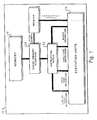
- data processing system 10 includes a memory 18 which is utilized to store data, instructions and the like. Data or instructions stored within memory 18 are preferably accessed utilizing cache/memory interface 20 in manner well known to those having skill in the art.
- cache/memory interface 20 The sizing and utilization of cache memory systems is a well known subspeciality within the data processing art and is not addressed within the present application. However, those skilled in the art will appreciate that by utilizing modern associative cache techniques, a large percentage of memory accesses may be achieved utilizing data temporarily stored within cache/memory interface 20.
- Instructions from cache/memory interface 20 are typically loaded into instruction dispatcher 22 which preferably includes a plurality of queue positions.
- instruction dispatcher 22 preferably includes a plurality of queue positions.
- each position within the instruction dispatch may include between two and eight instructions and thus, in a given cycle, up to eight instructions may be loaded into instruction dispatcher 22, depending upon how many valid instructions are passed by cache/memory interface 20 and how much space is available within instruction dispatcher 22.
- instruction dispatcher 22 is utilized to dispatch instructions to execution units 24.
- data processing system 10 may include one or more floating point units, fixed point processor units, load/store units, and a branch processor unit, as a matter of design choice.
- instruction dispatcher 22 may dispatch multiple instructions during a single cycle, one to each execution unit.
- Execution units may include reservation stations which could permit dispatch of more than one instruction to a single execution unit during a single cycle, as a matter of design choice.
- multiple execution units in a superscalar processor may each receive multiple instructions in a single cycle.
- instructions may be dispatched to multiple execution units 24 associated with multiple processors.
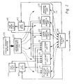
- FIG. 2 there is depicted a more detailed block diagram of the instruction dispatch circuitry of the superscalar data processing system of Figure 1 which may be utilized to implement the method and system of the present invention.
- instructions from cache/memory interface 20 are typically loaded into instruction dispatcher 22 in groups in an application specified sequential order.
- a group of two, four, or eight instructions are loaded from cache/memory interface 20 into instruction dispatcher 22, for dispatch on an opportunistic basis to one or more execution units within execution units 24.
- these execution units may include a floating point execution unit 26, multiple load/store units 28 and 30, multiple fixed point execution units 32 and 34, and a branch execution unit 36.
- a greater or lesser number of execution units of different types may be included within data processing system 10 as a matter of design choice.
- a plurality of general purpose registers are also provided.
- two groups of general purpose registers are provided.
- the results of the execution of multiple instructions within the execution units depicted within Figure 2 are typically stored within a selected general purpose register for future utilization.
- a plurality of intermediate storage buffers are also provided. That is, floating point intermediate storage buffers 40 and fixed point intermediate storage buffers 42.
- each execution unit is connected to each intermediate storage buffer via an independent bus.
- data required by an execution unit, or generated by the execution of an instruction within an execution unit may be placed on an independent bus and stored within a designated intermediate storage buffer for utilization by other execution units or for future transfer to a general purpose register.
- an intermediate storage buffer may be efficiently assigned to be immediately utilized as a storage location for a destination operand, permitting the instruction to be dispatched within a single processor cycle, since data locations do not need to be determined within a renamed register file.
- the execution of instructions in a non-sequential manner may be permitted, with the output of those instructions being temporarily stored within intermediate storage buffers for future assembly within the general purpose registers in the application specified sequential order.
- the fixed point execution units are each coupled via an independent bus to fixed point intermediate storage buffers 42, while the floating point execution unit is connected to each floating point intermediate storage buffer 40, via an independent bus.
- Load/store units 28 and 30, as those skilled in the art will appreciate, are necessarily connected to floating point intermediate storage buffers 40 and fixed point intermediate storage buffers 42, since these units will load and store both fixed point and floating point data.
- a completion buffer 48 is provided.
- Completion buffer 48 is utilized to track the completion of the multiple scalar instructions which are being executed within execution units 24. The results of the execution of these instructions, as described above, are each temporarily stored within an associated intermediate storage buffer and, upon an indication that an instruction or a group of instructions have been completed successfully, in an application specified sequential order, completion buffer 48 may be utilized to initiate the transfer of the results of those completed instructions data to the associated general purpose registers.
- completion buffer 48 may be utilized to initiate storage of the results of the execution of any instruction which completed prior to the exception and to control instruction dispatcher 22 to restart the process at the point where the exception condition occurred, permitting corrupted or invalid data to be replaced by a valid output in an efficient manner, or to initiate a new sequence of instructions as specified by the application specific program for specific types of exceptions.
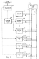
- FIG. 3 there is depicted a high level block diagram illustrating the utilization of intermediate storage buffers within the superscalar processor system of Figure 1, in accordance with the method and system of the present invention.
- a storage buffer index 58 is provided which is accessible by instruction dispatcher 22. As will be described in greater detail herein, storage buffer index 58 is utilized to store and maintain an indication of the relationship between each of a plurality of intermediate storage buffers 60 and a designated general purpose register 62 for utilization during execution of succeeding instructions.
- the plurality of intermediate storage buffers 60 are preferably connected to multiple independent buses 64.
- the number of independent buses 64 equals the number of intermediate storage buffers 60, with each intermediate storage buffer connected to one bus.
- Each of the intermediate storage buffers 60 may read from and write to a corresponding independent bus 64.
- the number of buses utilized may vary as a matter of design choice.
- execution units 24a, 24b, 24c are coupled to each of the multiple independent buses 64.
- execution units 24a, 24b, 24c may include a floating point execution unit, multiple load/store units, multiple fixed point execution units, and a branch execution unit.
- floating point execution unit may include a floating point execution unit, multiple load/store units, multiple fixed point execution units, and a branch execution unit.
- branch execution unit may include a branch execution unit.
- Each of the plurality of execution units 24a, 24b, 24c may also read from and write to each of the independent buses 64. Consequently, each of the plurality of execution units 24a, 24b, 24c are coupled to each of the plurality of intermediate storage buffers 60 via the multiple independent buses 64.
- the execution unit may place that data on a bus corresponding to a designated intermediate storage buffer which has been specified as a destination for that data, where the data may be temporarily stored.
- the execution unit indicates the data on the bus is valid by setting a "valid" bit to an appropriate state.
- any other execution unit which requires that data may retrieve the data from the bus.
- one advantage of the provision of independent buses is the elimination of the need to store the data in a buffer and then thereafter access that data from the buffer. The ability to retrieve data directly from the bus will significantly increase the operation speed of the processor system.
- multiple independent buses 64 are each coupled to general purpose registers 62.
- the relationship between the designated intermediate storage buffer and the selected general purpose register is preferably stored within the storage buffer index 58.
- the transfer of those results may be performed utilizing the information within storage buffer index 58.
- the information stored within storage buffer index 58 may be an identifier for the designated intermediate storage buffer which is accessed utilizing the general purpose register identification or an identifier of a general purpose register which is accessed with the identification of the designated intermediate storage buffer.
- storage buffer index 58 permits the execution of instructions in a non-sequential manner, since the results of execution of each instruction are temporarily stored in intermediate storage buffers 60, and may be subsequently utilized by a succeeding instruction by utilizing the information within storage buffer index 58 and the content of completion buffer 48 (see Figure 2).
- FIG 4 is a pictorial representation of a storage buffer index within the superscalar processor system of Figure 3 which may be utilized to implement the method and system of the present invention.
- Storage buffer index 58 comprises a number of entries, numbered 0-r. R equals the number of general purpose registers in the superscalar processor system.
- R equals the number of general purpose registers in the superscalar processor system.
- entry position 0 which corresponds to general purpose register 0
- entry position r which corresponds to general purpose register r
- an identifier for intermediate storage buffer 2 has been stored.
- FIG. 5 is a pictorial representation of an alternative storage buffer index within the superscalar processor system of Figure 3 which may be utilized to implement the method and system of the present invention.
- Storage buffer index 58 comprises a number of entries, numbered 0-n. N equals the number of intermediate storage buffers in the superscalar processor system.
- entry position 0 which corresponds to intermediate storage buffer 0
- an identifier for general purpose register 25 has been stored.
- entry position 2 which corresponds to intermediate storage buffer 2
- an identifier for general purpose register 2 has been stored.
Landscapes
- Engineering & Computer Science (AREA)
- Software Systems (AREA)
- Theoretical Computer Science (AREA)
- Physics & Mathematics (AREA)
- General Engineering & Computer Science (AREA)
- General Physics & Mathematics (AREA)
- Advance Control (AREA)
- Memory System Of A Hierarchy Structure (AREA)
- Executing Machine-Instructions (AREA)
Claims (6)
- Verfahren zur verbesserten Befehlszuteilung in einem superskalaren Prozessorsystem (10), das in der Lage ist, einer Vielzahl Befehlsausführungseinheiten (24) aus einem Zuteilungspuffer (22) eine Vielzahl skalarer Befehle zuzuteilen, wobei jeder aus der Vielzahl der skalaren Befehle mindestens einen Quelloperanden und einen Zieloperanden einschließt, wobei die Ergebnisse der Ausführung der Vielzahl der skalaren Befehle in einer Vielzahl Universalregister (62) gespeichert werden, wobei das Verfahren die folgenden Schritte umfaßt:Zuordnen eines speziellen Puffers aus der Vielzahl der Zwischenspeicherpuffer (60) zu einem Zieloperanden eines ausgewählten Befehls aus der Vielzahl der skalaren Befehle;Speichern eines Zusammenhanges zwischen dem speziellen Puffer aus der Vielzahl der Zwischenspeicherpuffer (60) und einem zugeordneten Register aus der Vielzahl der Universalregister (62) in einem Pufferindex (58);Speichern der Ergebnisse der Ausführung des ausgewählten Befehls aus der Vielzahl der skalaren Befehle in dem speziellen Puffer aus der Vielzahl der Zwischenspeicherpuffer (60); undÜbertragen der Ergebnisse der Befehlsausführung aus dem speziellen Puffer aus der Vielzahl der Zwischenspeicherpuffer (60) in eine andere Einheit aus der Vielzahl der Befehlsausführungseinheiten (24) zur Verwendung zur Ausführung eines anderen Befehls aus der Vielzahl der skalaren Befehle unter Benutzung des Pufferindex (58).
- Verfahren zur verbesserten Befehlszuteilung in einem superskalaren Prozessorsystem (10) gemäß Anspruch 1, wobei der Schritt des Speicherns eines Zusammenhanges zwischen dem speziellen Puffer aus der Vielzahl der Zwischenspeicherpuffer (60) und einem zugeordneten Register aus der Vielzahl der Universalregister (62) in einem Pufferindex (58) das Speichern eines Bezeichners für den speziellen Puffer aus der Vielzahl der Zwischenspeicherpuffer (60) in dem Pufferindex (58) und das Zugreifen auf den Bezeichner für den speziellen Puffer aus der Vielzahl der Zwischenspeicherpuffer (60) vom Pufferindex (58) aus unter Verwendung eines Bezeichners für das speziell zugeordnete Register aus der Vielzahl der Universalregister (62) umfaßt.
- Verfahren zur verbesserten Befehlszuteilung in einem superskalaren Prozessorsystem (10) gemäß Anspruch 1, wobei der Schritt des Speicherns eines Zusammenhanges zwischen dem speziellen Puffer aus der Vielzahl der Zwischenspeicherpuffer (60) und einem zugeordneten Register aus der Vielzahl der Universalregister (62) in einem Pufferindex (58) das Speichern eines Bezeichners für das zugeordnete Register aus der Vielzahl der Universalregister (62) in dem Pufferindex (58) und das Zugreifen auf den Bezeichner für das zugeordnete Register aus der Vielzahl der Universalregister (62) vom Pufferindex (58) aus unter Verwendung eines Bezeichners für den speziellen Puffer aus der Vielzahl der Zwischenspeicherpuffer (60) umfaßt.
- System zur verbesserten Befehlszuteilung in einem superskalaren Prozessorsystem (10), das in der Lage ist, einer Vielzahl Befehlsausführungseinheiten (24) aus einem Zuteilungspuffer (22) eine Vielzahl skalarer Befehle zuzuteilen, wobei jeder aus der Vielzahl der skalaren Befehle mindestens einen Quelloperanden und einen Zieloperanden einschließt, wobei die Ergebnisse der Ausführung der Vielzahl der skalaren Befehle in einer Vielzahl Universalregister (62) gespeichert werden, wobei das System umfaßt:Mittel zum Zuordnen eines speziellen Puffers aus der Vielzahl der Zwischenspeicherpuffer (60) zu einem Zieloperanden eines ausgewählten Befehls aus der Vielzahl der skalaren Befehle;Mittel zum Speichern eines Zusammenhanges zwischen dem speziellen Puffer aus der Vielzahl der Zwischenspeicherpuffer (60) und einem zugeordneten Register aus der Vielzahl der Universalregister (62) in einem Pufferindex (58);Mittel zum Speichern der Ergebnisse der Ausführung des ausgewählten Befehls aus der Vielzahl der skalaren Befehle in dem speziellen Puffer aus der Vielzahl der Zwischenspeicherpuffer (60); undMittel zum Übertragen der Ergebnisse der Befehlsausführung aus dem speziellen Puffer aus der Vielzahl der Zwischenspeicherpuffer (60) in eine andere Einheit aus der Vielzahl der Befehlsausführungseinheiten (24) zur Verwendung zur Ausführung eines anderen Befehls aus der Vielzahl der skalaren Befehle unter Benutzung des Pufferindex (58).
- System zur verbesserten Befehlszuteilung in einem superskalaren Prozessorsystem (10) gemäß Anspruch 4, wobei das Mittel zum Speichern eines Zusammenhanges zwischen dem speziellen Puffer aus der Vielzahl der Zwischenspeicherpuffer (60) und einem zugeordneten Register aus der Vielzahl der Universalregister (62) in einem Pufferindex (58) ein Mittel zum Speichern eines Bezeichners für den speziellen Puffer aus der Vielzahl der Zwischenspeicherpuffer (60) in dem Pufferindex (58) und ein Mittel zum Zugreifen auf den Bezeichner für den speziellen Puffer aus der Vielzahl der Zwischenspeicherpuffer (60) vom Pufferindex (58) aus unter Verwendung eines Bezeichners für das speziell zugeordnete Register aus der Vielzahl der Universalregister (62) umfaßt.
- System zur verbesserten Befehlszuteilung in einem superskalaren Prozessorsystem (10) gemäß Anspruch 4, wobei das Mittel zum Speichern eines Zusammenhanges zwischen dem speziellen Puffer aus der Vielzahl der Zwischenspeicherpuffer (60) und einem zugeordneten Register aus der Vielzahl der Universalregister (62) in einem Pufferindex (58) ein Mittel zum Speichern eines Bezeichners für das zugeordnete Register aus der Vielzahl der Universalregister (62) in dem Pufferindex (58) und ein Mittel zum Zugreifen auf den Bezeichner für das zugeordnete Register aus der Vielzahl der Universalregister (62) vom Pufferindex (58) aus unter Verwendung eines Bezeichners für den speziellen Puffer aus der Vielzahl der Zwischenspeicherpuffer (60) umfaßt.
Applications Claiming Priority (2)
| Application Number | Priority Date | Filing Date | Title |
|---|---|---|---|
| US187293A | 1993-01-08 | 1993-01-08 | |
| US1872 | 1997-12-31 |
Publications (2)
| Publication Number | Publication Date |
|---|---|
| EP0605868A1 EP0605868A1 (de) | 1994-07-13 |
| EP0605868B1 true EP0605868B1 (de) | 1998-11-04 |
Family
ID=21698213
Family Applications (1)
| Application Number | Title | Priority Date | Filing Date |
|---|---|---|---|
| EP93120933A Expired - Lifetime EP0605868B1 (de) | 1993-01-08 | 1993-12-27 | Verfahren und System um einen unabhängige Zugriff auf Zwischenspeicherpuffern in einem superskalaren Prozessorsystem zu gewährleisten. |
Country Status (9)
| Country | Link |
|---|---|
| US (1) | US5491829A (de) |
| EP (1) | EP0605868B1 (de) |
| JP (1) | JP2777535B2 (de) |
| KR (1) | KR0122528B1 (de) |
| CN (1) | CN1042863C (de) |
| AT (1) | ATE173100T1 (de) |
| CA (1) | CA2112995A1 (de) |
| DE (1) | DE69321929T2 (de) |
| TW (1) | TW230807B (de) |
Families Citing this family (25)
| Publication number | Priority date | Publication date | Assignee | Title |
|---|---|---|---|---|
| TW242673B (de) * | 1993-08-18 | 1995-03-11 | Ibm | |
| US6378062B1 (en) * | 1994-01-04 | 2002-04-23 | Intel Corporation | Method and apparatus for performing a store operation |
| CN1326033C (zh) | 1994-12-02 | 2007-07-11 | 英特尔公司 | 可以对复合操作数进行压缩操作的微处理器 |
| FR2731094B1 (fr) * | 1995-02-23 | 1997-04-30 | Dufal Frederic | Procede et dispositif de commande simultanee des etats de controle des unites d'execution d'un processeur programmable |
| JP2636789B2 (ja) * | 1995-03-31 | 1997-07-30 | 日本電気株式会社 | マイクロプロセッサ |
| US5974240A (en) * | 1995-06-07 | 1999-10-26 | International Business Machines Corporation | Method and system for buffering condition code data in a data processing system having out-of-order and speculative instruction execution |
| US5875294A (en) | 1995-06-30 | 1999-02-23 | International Business Machines Corporation | Method and system for halting processor execution in response to an enumerated occurrence of a selected combination of internal states |
| US5949971A (en) * | 1995-10-02 | 1999-09-07 | International Business Machines Corporation | Method and system for performance monitoring through identification of frequency and length of time of execution of serialization instructions in a processing system |
| US5764970A (en) * | 1995-11-20 | 1998-06-09 | International Business Machines Corporation | Method and apparatus for supporting speculative branch and link/branch on count instructions |
| US6792523B1 (en) | 1995-12-19 | 2004-09-14 | Intel Corporation | Processor with instructions that operate on different data types stored in the same single logical register file |
| US5701508A (en) | 1995-12-19 | 1997-12-23 | Intel Corporation | Executing different instructions that cause different data type operations to be performed on single logical register file |
| US5852726A (en) * | 1995-12-19 | 1998-12-22 | Intel Corporation | Method and apparatus for executing two types of instructions that specify registers of a shared logical register file in a stack and a non-stack referenced manner |
| US5940859A (en) | 1995-12-19 | 1999-08-17 | Intel Corporation | Emptying packed data state during execution of packed data instructions |
| US5845149A (en) * | 1996-04-10 | 1998-12-01 | Allen Bradley Company, Llc | Industrial controller with I/O mapping table for linking software addresses to physical network addresses |
| US6298435B1 (en) * | 1996-04-16 | 2001-10-02 | International Business Machines Corporation | Methods and apparatus for exploiting virtual buffers to increase instruction parallelism in a pipelined processor |
| US5805907A (en) * | 1996-10-04 | 1998-09-08 | International Business Machines Corporation | System and method for reducing power consumption in an electronic circuit |
| US5870616A (en) * | 1996-10-04 | 1999-02-09 | International Business Machines Corporation | System and method for reducing power consumption in an electronic circuit |
| US5765017A (en) * | 1997-01-13 | 1998-06-09 | International Business Machines Corporation | Method and system in a data processing system for efficient management of an indication of a status of each of multiple registers |
| US5974538A (en) * | 1997-02-21 | 1999-10-26 | Wilmot, Ii; Richard Byron | Method and apparatus for annotating operands in a computer system with source instruction identifiers |
| US5875326A (en) * | 1997-04-25 | 1999-02-23 | International Business Machines Corporation | Data processing system and method for completing out-of-order instructions |
| JP2001092657A (ja) * | 1999-09-22 | 2001-04-06 | Toshiba Corp | 中央演算装置、コンパイル方法、及びコンパイルプログラムを記録した記録媒体 |
| US7039060B2 (en) * | 2001-03-07 | 2006-05-02 | Mips Tech Inc | System and method for extracting fields from packets having fields spread over more than one register |
| US6826704B1 (en) * | 2001-03-08 | 2004-11-30 | Advanced Micro Devices, Inc. | Microprocessor employing a performance throttling mechanism for power management |
| US7330988B2 (en) * | 2004-06-30 | 2008-02-12 | Sun Microsystems, Inc. | Method and apparatus for power throttling in a multi-thread processor |
| CN100576169C (zh) * | 2007-07-11 | 2009-12-30 | 凌阳科技股份有限公司 | 一种执行指令的方法及系统 |
Family Cites Families (10)
| Publication number | Priority date | Publication date | Assignee | Title |
|---|---|---|---|---|
| JPS581246A (ja) * | 1981-06-26 | 1983-01-06 | Fujitsu Ltd | 命令処理順序制御方式 |
| JPS58178464A (ja) * | 1982-04-14 | 1983-10-19 | Hitachi Ltd | 並列演算処理装置 |
| US4594660A (en) * | 1982-10-13 | 1986-06-10 | Honeywell Information Systems Inc. | Collector |
| US5067069A (en) * | 1989-02-03 | 1991-11-19 | Digital Equipment Corporation | Control of multiple functional units with parallel operation in a microcoded execution unit |
| WO1990010267A1 (en) * | 1989-02-24 | 1990-09-07 | Nexgen Microsystems | Distributed pipeline control for a computer |
| JP2825906B2 (ja) * | 1990-02-01 | 1998-11-18 | 株式会社日立製作所 | 計算機システム |
| US5237694A (en) * | 1991-05-30 | 1993-08-17 | Advanced Micro Devices, Inc. | Processing system and method including lock buffer for controlling exclusive critical problem accesses by each processor |
| US5345569A (en) * | 1991-09-20 | 1994-09-06 | Advanced Micro Devices, Inc. | Apparatus and method for resolving dependencies among a plurality of instructions within a storage device |
| US5416913A (en) * | 1992-07-27 | 1995-05-16 | Intel Corporation | Method and apparatus for dependency checking in a multi-pipelined microprocessor |
| US5367650A (en) * | 1992-07-31 | 1994-11-22 | Intel Corporation | Method and apparauts for parallel exchange operation in a pipelined processor |
-
1993
- 1993-12-20 KR KR1019930028551A patent/KR0122528B1/ko not_active Expired - Fee Related
- 1993-12-22 JP JP5325254A patent/JP2777535B2/ja not_active Expired - Lifetime
- 1993-12-27 EP EP93120933A patent/EP0605868B1/de not_active Expired - Lifetime
- 1993-12-27 AT AT93120933T patent/ATE173100T1/de not_active IP Right Cessation
- 1993-12-27 DE DE69321929T patent/DE69321929T2/de not_active Expired - Fee Related
- 1993-12-29 TW TW082111133A patent/TW230807B/zh active
-
1994
- 1994-01-06 CA CA002112995A patent/CA2112995A1/en not_active Abandoned
- 1994-01-08 CN CN94100120A patent/CN1042863C/zh not_active Expired - Fee Related
-
1995
- 1995-05-11 US US08/438,819 patent/US5491829A/en not_active Expired - Fee Related
Also Published As
| Publication number | Publication date |
|---|---|
| DE69321929T2 (de) | 1999-07-01 |
| CA2112995A1 (en) | 1994-07-09 |
| US5491829A (en) | 1996-02-13 |
| KR940018757A (ko) | 1994-08-18 |
| TW230807B (de) | 1994-09-21 |
| EP0605868A1 (de) | 1994-07-13 |
| ATE173100T1 (de) | 1998-11-15 |
| KR0122528B1 (ko) | 1997-11-20 |
| DE69321929D1 (de) | 1998-12-10 |
| JPH06242955A (ja) | 1994-09-02 |
| CN1092189A (zh) | 1994-09-14 |
| CN1042863C (zh) | 1999-04-07 |
| JP2777535B2 (ja) | 1998-07-16 |
Similar Documents
| Publication | Publication Date | Title |
|---|---|---|
| EP0605868B1 (de) | Verfahren und System um einen unabhängige Zugriff auf Zwischenspeicherpuffern in einem superskalaren Prozessorsystem zu gewährleisten. | |
| EP0605875B1 (de) | Verfahren und System zur Zuteilung mehrerer Befehle in einem superskalaren Prozessorsystem in einem einzigen Zyklus | |
| EP0605866B1 (de) | Verfahren und System zur Befehlszuteilung in einem superskalaren Prozessorsystem mit unabhängig zugänglichem Zwischenspeicher | |
| US5611063A (en) | Method for executing speculative load instructions in high-performance processors | |
| EP0762270B1 (de) | Mikroprozessor mit Lade-/Speicheroperation zu/von mehreren Registern | |
| US6209081B1 (en) | Method and system for nonsequential instruction dispatch and execution in a superscalar processor system | |
| JP3207124B2 (ja) | カウント/リンク・レジスタ変更命令の投機実行をサポートする方法及び装置 | |
| EP0605867A1 (de) | Verfahren und System zur auswählenden reihenweisen Befehlsausführung im superskalaren Prozessorsystem | |
| US5761473A (en) | Method and system for increased instruction synchronization efficiency in a superscalar processsor system utilizing partial data dependency interlocking | |
| EP0605873A1 (de) | Verfahren und System zur Überwachung von Skalarbefehlen im superskalaren Prozessorsystem | |
| US5758117A (en) | Method and system for efficiently utilizing rename buffers to reduce dispatch unit stalls in a superscalar processor | |
| EP0495162A2 (de) | Speicherverwaltung |
Legal Events
| Date | Code | Title | Description |
|---|---|---|---|
| PUAI | Public reference made under article 153(3) epc to a published international application that has entered the european phase |
Free format text: ORIGINAL CODE: 0009012 |
|
| AK | Designated contracting states |
Kind code of ref document: A1 Designated state(s): AT BE CH DE ES FR GB IT LI NL SE |
|
| 17P | Request for examination filed |
Effective date: 19941125 |
|
| GRAG | Despatch of communication of intention to grant |
Free format text: ORIGINAL CODE: EPIDOS AGRA |
|
| 17Q | First examination report despatched |
Effective date: 19980123 |
|
| GRAG | Despatch of communication of intention to grant |
Free format text: ORIGINAL CODE: EPIDOS AGRA |
|
| GRAH | Despatch of communication of intention to grant a patent |
Free format text: ORIGINAL CODE: EPIDOS IGRA |
|
| GRAH | Despatch of communication of intention to grant a patent |
Free format text: ORIGINAL CODE: EPIDOS IGRA |
|
| GRAA | (expected) grant |
Free format text: ORIGINAL CODE: 0009210 |
|
| AK | Designated contracting states |
Kind code of ref document: B1 Designated state(s): AT BE CH DE ES FR GB IT LI NL SE |
|
| PG25 | Lapsed in a contracting state [announced via postgrant information from national office to epo] |
Ref country code: SE Free format text: THE PATENT HAS BEEN ANNULLED BY A DECISION OF A NATIONAL AUTHORITY Effective date: 19981104 Ref country code: ES Free format text: THE PATENT HAS BEEN ANNULLED BY A DECISION OF A NATIONAL AUTHORITY Effective date: 19981104 Ref country code: AT Free format text: LAPSE BECAUSE OF FAILURE TO SUBMIT A TRANSLATION OF THE DESCRIPTION OR TO PAY THE FEE WITHIN THE PRESCRIBED TIME-LIMIT Effective date: 19981104 |
|
| REF | Corresponds to: |
Ref document number: 173100 Country of ref document: AT Date of ref document: 19981115 Kind code of ref document: T |
|
| REG | Reference to a national code |
Ref country code: CH Ref legal event code: EP |
|
| REF | Corresponds to: |
Ref document number: 69321929 Country of ref document: DE Date of ref document: 19981210 |
|
| PG25 | Lapsed in a contracting state [announced via postgrant information from national office to epo] |
Ref country code: LI Free format text: LAPSE BECAUSE OF NON-PAYMENT OF DUE FEES Effective date: 19981231 Ref country code: CH Free format text: LAPSE BECAUSE OF NON-PAYMENT OF DUE FEES Effective date: 19981231 |
|
| ITF | It: translation for a ep patent filed | ||
| REG | Reference to a national code |
Ref country code: CH Ref legal event code: NV Representative=s name: DIPL.-ING. CHRISTIAN HEUSCH C/O INTERNATIONAL BUSI |
|
| ET | Fr: translation filed | ||
| REG | Reference to a national code |
Ref country code: CH Ref legal event code: PL |
|
| PLBE | No opposition filed within time limit |
Free format text: ORIGINAL CODE: 0009261 |
|
| STAA | Information on the status of an ep patent application or granted ep patent |
Free format text: STATUS: NO OPPOSITION FILED WITHIN TIME LIMIT |
|
| 26N | No opposition filed | ||
| PGFP | Annual fee paid to national office [announced via postgrant information from national office to epo] |
Ref country code: BE Payment date: 19991112 Year of fee payment: 7 |
|
| PGFP | Annual fee paid to national office [announced via postgrant information from national office to epo] |
Ref country code: NL Payment date: 19991231 Year of fee payment: 7 |
|
| PGFP | Annual fee paid to national office [announced via postgrant information from national office to epo] |
Ref country code: DE Payment date: 20001201 Year of fee payment: 8 |
|
| PGFP | Annual fee paid to national office [announced via postgrant information from national office to epo] |
Ref country code: FR Payment date: 20001220 Year of fee payment: 8 |
|
| PG25 | Lapsed in a contracting state [announced via postgrant information from national office to epo] |
Ref country code: BE Free format text: LAPSE BECAUSE OF NON-PAYMENT OF DUE FEES Effective date: 20001231 |
|
| BERE | Be: lapsed |
Owner name: INTERNATIONAL BUSINESS MACHINES CORP. Effective date: 20001231 |
|
| PG25 | Lapsed in a contracting state [announced via postgrant information from national office to epo] |
Ref country code: NL Free format text: LAPSE BECAUSE OF NON-PAYMENT OF DUE FEES Effective date: 20010701 |
|
| NLV4 | Nl: lapsed or anulled due to non-payment of the annual fee |
Effective date: 20010701 |
|
| PGFP | Annual fee paid to national office [announced via postgrant information from national office to epo] |
Ref country code: GB Payment date: 20011210 Year of fee payment: 9 |
|
| REG | Reference to a national code |
Ref country code: GB Ref legal event code: IF02 |
|
| PG25 | Lapsed in a contracting state [announced via postgrant information from national office to epo] |
Ref country code: DE Free format text: LAPSE BECAUSE OF NON-PAYMENT OF DUE FEES Effective date: 20020702 |
|
| PG25 | Lapsed in a contracting state [announced via postgrant information from national office to epo] |
Ref country code: FR Free format text: LAPSE BECAUSE OF NON-PAYMENT OF DUE FEES Effective date: 20020830 |
|
| REG | Reference to a national code |
Ref country code: FR Ref legal event code: ST |
|
| PG25 | Lapsed in a contracting state [announced via postgrant information from national office to epo] |
Ref country code: GB Free format text: LAPSE BECAUSE OF NON-PAYMENT OF DUE FEES Effective date: 20021227 |
|
| GBPC | Gb: european patent ceased through non-payment of renewal fee |
Effective date: 20021227 |
|
| PG25 | Lapsed in a contracting state [announced via postgrant information from national office to epo] |
Ref country code: IT Free format text: LAPSE BECAUSE OF NON-PAYMENT OF DUE FEES;WARNING: LAPSES OF ITALIAN PATENTS WITH EFFECTIVE DATE BEFORE 2007 MAY HAVE OCCURRED AT ANY TIME BEFORE 2007. THE CORRECT EFFECTIVE DATE MAY BE DIFFERENT FROM THE ONE RECORDED. Effective date: 20051227 |