EP0605972A1 - Elément récepteur de lumière ayant une couche réceptrice de lumière à structure multiple avec une concentration améliorée en atomes d'hydrogène ou/et d'halogène à proximité de l'interface des couches adjacentes - Google Patents
Elément récepteur de lumière ayant une couche réceptrice de lumière à structure multiple avec une concentration améliorée en atomes d'hydrogène ou/et d'halogène à proximité de l'interface des couches adjacentes Download PDFInfo
- Publication number
- EP0605972A1 EP0605972A1 EP93310038A EP93310038A EP0605972A1 EP 0605972 A1 EP0605972 A1 EP 0605972A1 EP 93310038 A EP93310038 A EP 93310038A EP 93310038 A EP93310038 A EP 93310038A EP 0605972 A1 EP0605972 A1 EP 0605972A1
- Authority
- EP
- European Patent Office
- Prior art keywords
- layer
- light receiving
- receiving member
- atoms
- region
- Prior art date
- Legal status (The legal status is an assumption and is not a legal conclusion. Google has not performed a legal analysis and makes no representation as to the accuracy of the status listed.)
- Granted
Links
Images


Classifications
-
- G—PHYSICS
- G03—PHOTOGRAPHY; CINEMATOGRAPHY; ANALOGOUS TECHNIQUES USING WAVES OTHER THAN OPTICAL WAVES; ELECTROGRAPHY; HOLOGRAPHY
- G03G—ELECTROGRAPHY; ELECTROPHOTOGRAPHY; MAGNETOGRAPHY
- G03G5/00—Recording-members for original recording by exposure, e.g. to light, to heat or to electrons; Manufacture thereof; Selection of materials therefor
- G03G5/02—Charge-receiving layers
- G03G5/04—Photoconductive layers; Charge-generation layers or charge-transporting layers; Additives therefor; Binders therefor
- G03G5/08—Photoconductive layers; Charge-generation layers or charge-transporting layers; Additives therefor; Binders therefor characterised by the photoconductive material being inorganic
- G03G5/082—Photoconductive layers; Charge-generation layers or charge-transporting layers; Additives therefor; Binders therefor characterised by the photoconductive material being inorganic and not being incorporated in a bonding material, e.g. vacuum deposited
- G03G5/08214—Silicon-based
- G03G5/08221—Silicon-based comprising one or two silicon based layers
- G03G5/08228—Silicon-based comprising one or two silicon based layers at least one with varying composition
-
- G—PHYSICS
- G03—PHOTOGRAPHY; CINEMATOGRAPHY; ANALOGOUS TECHNIQUES USING WAVES OTHER THAN OPTICAL WAVES; ELECTROGRAPHY; HOLOGRAPHY
- G03G—ELECTROGRAPHY; ELECTROPHOTOGRAPHY; MAGNETOGRAPHY
- G03G5/00—Recording-members for original recording by exposure, e.g. to light, to heat or to electrons; Manufacture thereof; Selection of materials therefor
- G03G5/02—Charge-receiving layers
- G03G5/04—Photoconductive layers; Charge-generation layers or charge-transporting layers; Additives therefor; Binders therefor
- G03G5/08—Photoconductive layers; Charge-generation layers or charge-transporting layers; Additives therefor; Binders therefor characterised by the photoconductive material being inorganic
- G03G5/082—Photoconductive layers; Charge-generation layers or charge-transporting layers; Additives therefor; Binders therefor characterised by the photoconductive material being inorganic and not being incorporated in a bonding material, e.g. vacuum deposited
- G03G5/08214—Silicon-based
- G03G5/08235—Silicon-based comprising three or four silicon-based layers
- G03G5/08242—Silicon-based comprising three or four silicon-based layers at least one with varying composition
Definitions
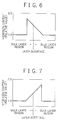
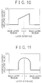
- FIG. 5 is a schematic diagram showing a second pattern of the concentration distribution of hydrogen atoms in the vicinity of the interface between the adjacent layers of a light receiving member according to the present invention.
- Non-single crystal material containing silicon atoms, hydrogen atoms and/or halogen atoms such as a-Si:H material, a-Si:X material (X is halogen atom), or polycrystalline silicon material (these materials will be hereinafter referred to as "non-single crystal Si:(H,X) material” or “nc-Si:(H,X) material”).
- the light receiving member according to the present invention basically comprises a substrate and a light receiving layer having a stacked structure disposed on said substrate, said stacked structure comprising at least two layers each being constituted by a non-single crystal material containing silicon atoms as a matrix and at least one kind of atoms selected from hydrogen atoms and halogen atoms (hereinafter referred to as nc-Si (H,X) material).
- nc-Si (H,X) material hereinafter referred to as nc-Si (H,X) material.
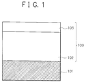
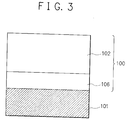
- the receiving member having the nc-Si (H,X) light receiving layer according to the present invention may take such a constitution as shown in FIG. 1, 2 or 3. It should be understood that the light receiving member according to the present invention is not restricted to these constitutions shown in FIGs. 1 to 3 only, but it may take other appropriate constitutions.
- the light receiving member shown in FIG. 2 is a modification of the light receiving member shown in FIG. 1 in which the un-Si (H,X) photoconductive layer in FIG. 1 is replaced by a function-divided type light receiving layer 102 comprising a charge transportation layer 104 and a charge generation layer 105 each being constituted by a nc-Si (H,X) material.
- the hydrogen atoms (H) or/and halogen atoms contained in the light receiving layer 100 are specifically designed as will be described below.
- the hydrogen atoms (H) or/and halogen atoms (X) are contained in each of the charge transportation layer 104 and the charge generation layer 105 such that their concentration distribution is uniform in the direction in parallel to the surface of the substrate 101 and their concentration distribution in the thickness direction is enhanced to be greater than the content of these atoms in the bulk layer region of each of the charge transportation layer and the charge generation layer in the neighborhood region of the interface between the two layers.
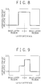
- the hydrogen concentration distribution pattern may be such a pattern as shown in any of FIGs. 6 to 11.
- the concentration distribution of the hydrogen atoms (H) or/and halogen atoms (X) contained in the bulk layer region of each adjacent layer it should be properly determined depending upon the related factors such as the functions required for a light receiving member to be produced, the kind of a manufacturing apparatus used, and the like.
- the multi-layered light receiving layer becomes poor in terms of structural stability and also in terms of quality.
- the neighborhood region contains the hydrogen atoms in an excessive amount which is larger that its amount required for attaining relaxation of a structural distortion, the networks among the silicon atoms in the layer structure become liable to derange or break, resulting in making the layer structure unstable.
- the content of the hydrogen atoms (H) or/and halogen atoms (X) contained in the neighborhood region of the interface between the adjacent layers it is desired to be preferably 1.1 to 2 holds or most preferably 1.2 to 1.8 holds over that contained in the bulk layer regions of the adjacent layers.
- the thickness of the above neighborhood region it is desired to be preferably 100 to 10000 ⁇ , more preferably 100 to 5000 ⁇ or most preferably 500 to 3000 ⁇ in the thickness direction, centered on the interface between the adjacent layers.
- the content of the content of the hydrogen atoms (H) contained in each adjacent layer it should be decided while having a due care not only about the content in the region where it is maximized (that is, the layer interface neighborhood region) but also about that in each bulk layer region.
- the content of the hydrogen atoms (H) contained in the layer interface neighborhood region is to be preferably in the range of 0.1 to 45 atomic%, more preferably in the range of 1 to 40 atomic%, most preferably in the range of 3 to 35 atomic%, versus the amount of the entire constituent atoms thereof.
- each bulk layer region contains hydrogen atoms (H) contained in each bulk layer region.
- H hydrogen atoms
- the content thereof is desired to be preferably 0.5 atomic ppm to 30 atomic%, or more preferably 1 atomic ppm to 20 atomic%, versus the amount of the entire constituent atoms thereof.
- the content of the halogen atoms (X) contained in the neighborhood region of the interface between the adjacent layers in the case where each bulk layer region is also incorporated with the halogen atoms (X), it is desired to be greater preferably by more than 1.1 holds, more preferably by more than 1.15 holds, or most preferably by more than 1.2 holds over the content thereof in the bulk layer region which is the greatest in terms of the halogen content.
- the thickness of the neighborhood region of the interface between the adjacent layers containing the halogen atoms (X) at an enhanced concentration distribution it is desired to be preferably 100 ⁇ to 1 ⁇ m, or more preferably 500 to 5000 ⁇ .
- a given region wherein the hydrogen atoms (H) or/and halogen atoms (X) are contained at an enhanced concentration distribution is desired to be of a thickness of 100 ⁇ to 1 ⁇ m as well as in the case where the neighborhood region of the interface between the adjacent layers is involved, in order to prevent the balk layer region of each adjacent layer from suffering a negative influence in terms of the inherent electric characteristics.
- the multi-layered light receiving layer comprises three or more nc-Si (H,X) constituent layers each having a different chemical composition and have two or more interfaces
- the above analysis method can include SIMS, infrared-absorbing analysis method, and thermal desorption analysis method.
- nuclear reaction method nuclear magnetic resonance method
- ESCA nuclear magnetic resonance method
- RBS Auger electron spectroscopy
- radiation chemical analysis method mass spectrometry
- absorptiometry absorptiometry
- gas analysis method can be used. These analysis methods can be used either singly or in combination of two or more of them.
- the thickness of the nc-Si (H,X) layer having photoconductivity (that is, the photoconductive layer 102; see, FIGs. 1 to 3) as one of the constituent layers of the nc-Si (H,X) multi-layered light receiving layer 100 is one of the important factors, in order to effectively attain the objects of the present invention, and a due care should be made thereof so that the resulting light receiving member provides desirable characteristics. In general, it is made to be in the range of 1 to 100 ⁇ m. However, it is made to be in the range of 1 to 80 ⁇ m in a preferred embodiment, and to be in the range of 2 to 50 ⁇ m in a more preferred embodiment.
- the light receiving layer of the light receiving member according to the present invention may contain atoms of a conductivity controlling element or/and at least one kind of atoms selected from the group consisting of oxygen atoms, carbon atoms and nitrogen atoms.
- the light receiving layer of the light receiving member according to the present invention is incorporated with atoms of a given conductivity controlling element
- the atoms may be contained in the entire layer region or in a partial layer region thereof such that they are uniformly or unevenly distributed in the thickness direction.
- Such conductivity controlling element can include so-called impurities used in the field of semiconductor such as elements capable of imparting a p-type conductivity which belong to group IIIB of the periodic table (hereinafter referred to as group IIIB element) and elements capable of imparting an n-type conductivity which belong to group VB of the periodic table (hereinafter referred to as group VB element).
- group IIIB element elements capable of imparting a p-type conductivity which belong to group IIIB of the periodic table
- group VB element elements capable of imparting an n-type conductivity which belong to group VB of the periodic table
- group VB element P, As, Sb, and Bi, and among these, P and Sb being the most desirable.
- a given element selected from the group consisting of the above group IIIB and group VB elements is contained in a partial layer region thereof adjacent to the substrate such that atoms of the element are uniformly distributed at a relatively high concentration, or a given element selected from the group consisting of the above group IIIB and group VB elements is contained in the photoconductive layer such that atoms of the element are contained therein so as to establish a concentration distribution in the thickness direction which is enhanced in a layer region of thereof situated on the substrate side, wherein any of the above layer regions each being incorporated with atoms of a given element selected from the group consisting of the above group IIIB and group VB elements at a high concentration functions as a charge injection inhibition layer.
- the thickness thereof is usually made to be at least 3 x 10 ⁇ 3 ⁇ m. However it is preferably in the range of 4 x 10 ⁇ 3 to 8 ⁇ m or more preferably in the range of 1 x 10 ⁇ 3 to 5 ⁇ m.
- the above group IIIB and VB elements may be selectively contained in the light receiving layer at a desired concentration distribution while taking into account the amount thereof depending upon the requirements for a light receiving member obtained.
- the photoconductive layer may be incorporated with a conductivity controlling element having a different polarity from that of the conductivity controlling element contained in the charge injection inhibition layer.
- both the photoconductive layer and charge injection inhibition layer are incorporated with the same conductivity controlling element and the content of the conductivity controlling element in the charge injection inhibition layer is significantly greater than that in the photoconductive layer.
- the concentration distribution for the conductivity controlling element contained in the multi-layered light receiving layer it is not always necessary for each layer to have an independent concentration gradient. It is possible for the multi-layered light receiving layer to contain the conductivity controlling element such that a desired concentration gradient is established in a given layer region or the entire layer region of the multi-layered light receiving layer. For instance, it is possible for the multi-layered light receiving layer to contain the conductivity controlling element such that the content of the conductivity controlling element in a layer region adjacent to the substrate is maximum and it decreases as the distance from the substrate increases or such that the content of the conductivity controlling element in a layer region adjacent to the substrate is minimum and it increases as the distance from the substrate increases. Other than these, it is possible that the conductivity controlling element is contained so as to have a maximum or minimum concentration value in a given layer region of the photoconductive layer.
- the surface layer 103 (see, FIGs. 1 and 2) of the light receiving member according to the present invention may comprise a nc-SiC:(H,X) material, nc-SiN:(H,X) material or nc-SiO:(H,X) material.
- This surface layer may contain atoms of an element belonging to group III of the periodic table (hereinafter referred to as group III element) or atoms of an element belonging to group V (excluding N) of the periodic table (hereinafter referred to as group V element) in such a state that the atoms are distributed either uniformly or unevenly in the thickness direction in the layer.
- the surface layer becomes to contain, in addition to the C, N or O, the atoms of the group III or V element in a desired distribution state.
- the electrical and photoconductive properties of the surface layer are controlled as desired.
- the concentration distribution state of the atoms of the group III or V element in the surface layer may be designed such that the content of the atoms is enhanced on the free surface side or it is enhanced on the photoconductive layer side.
- the multi-layered light receiving layer comprising a nc-Si:(H,X) material (including a-Si:(H,X) material) of the light receiving member according to the present invention may be formed by a conventional sputtering method, ion plating method, thermal-induced CVD method wherein raw material gas is thermally decomposed to form a deposited film on a substrate, photo-assisted CVD method wherein raw material gas is decomposed with the action of light energy to form a deposited film on a substrate, or plasma CVD method wherein direct current, high frequency or microwave grow discharge is caused to produce plasma whereby raw material gas is decomposed to form a deposited film on a substrate.
- To control the content of the hydrogen atoms (H) or/and halogen atoms (X) in the neighborhood region of the interface between adjacent nc-Si:(H,X) layers so as to provide a desired concentration distribution pattern can be conducted by an appropriate manner such as (i) a manner of adjusting the amount of these atoms contained by properly varying the flow rate for the foregoing hydrogen atom-supplying gaseous raw material or/and the foregoing halogen atom-supplying gaseous raw material to be introduced into the discharging space (that is, the deposition chamber), (ii) a manner of adjusting the amount of these atoms contained by properly varying the discharging power applied, (iii) a manner of adjusting the amount of these atoms by properly varying the bias voltage applied, (iv) a manner of adjusting the amount of these atoms contained by properly varying the inner pressure of the discharging space (that is, the deposition chamber), or (v) a manner of adjusting the amount of these atom
- the formation of said layer is conducted by using a Si-target comprising a single crystal or polycrystalline Si-wafer and introducing the foregoing gaseous halogen atom-supplying raw material and/or hydrogen gas, if necessary inert gas such as He or Ar in addition, into the deposition chamber having said Si-target placed therein, and generating a plasma to sputter the Si-target, to thereby form respective nc-Si:(H,X) layers on a substrate.
- a Si-target comprising a single crystal or polycrystalline Si-wafer and introducing the foregoing gaseous halogen atom-supplying raw material and/or hydrogen gas, if necessary inert gas such as He or Ar in addition, into the deposition chamber having said Si-target placed therein, and generating a plasma to sputter the Si-target, to thereby form respective nc-Si:(H,X) layers on a substrate.
- a given gaseous raw material capable of supplying the group IIIB or VB element is introduced into the deposition chamber while properly controlling the flow rate thereof as desired, together with the foregoing film-forming raw material gase upon conducting the formation of a nc-Si:(H,X) layer by the plasma CVD method in the manner as above described.
- a given gaseous raw material capable of supplying the group IIIB or VB element is introduced into the deposition chamber while controlling the flow rate thereof upon conducting the formation of a nc-Si:(H,X) layer by the sputtering method in the manner as above described.
- group IIIB element-supplying gaseous raw material examples include boron hydrides such as B2H6, B4H10, B5H9, B5H11, B6H10, B6H12, and B6H14, and boron halides such as BF3, BCl3, and BBr3.
- boron hydrides such as B2H6, B4H10, B5H9, B5H11, B6H10, B6H12, and B6H14
- boron halides such as BF3, BCl3, and BBr3.
- AlCl3, GaCl3, Ga(CH3)3, InCl3, and TlCl3 can also mentioned.
- group VB element-supplying gaseous raw material are phosphorous hydrides such as PH3, and P2H4, and phosphorous halides such as PH4I, PF3, PF5, PCl3, PCl5, PBr3, PBr5, and PI3.
- phosphorous hydrides such as PH3, and P2H4
- phosphorous halides such as PH4I, PF3, PF5, PCl3, PCl5, PBr3, PBr5, and PI3.
- AsH3, AsF3, AsCl3, AsBr3, AsF5, SbH3, SbF3, SbF5, SbCl3, SbCl5, BiH3, BiCl3, and BiBr3 can also be mentioned.
- nc-SiO:(H,X) layer or partial layer region containing oxygen atoms (O) (hereinafter referred to as nc-SiO:(H,X) layer or partial layer region) by the plasma CVD method)
- a gaseous raw material capable of supplying oxygen atoms (O) is introduced into the deposition chamber while properly controlling the flow rate thereof, together with the film-forming gaseous raw material upon forming the foregoing nc-Si:(H,X) layer by the plasma CVD method.
- the oxygen atom-supplying raw material (hereinafter referred to as O-supplying raw material) can include most of those gaseous or gasifiable materials which contain at least oxygen atoms as the constituent atoms.
- the raw material gases used in combination it is possible to employ, for example, a combination of a gaseous raw material containing silicon atoms (Si) as the constituent atoms, a gaseous raw material containing oxygen atoms (O) as the constituent atoms and as required, a gaseous raw material containing hydrogen atoms (H) and/or halogen atoms (X) as the constituent atoms in a desired mixing ratio; a combination of a gaseous raw material containing silicon atoms (Si) as the constituent atoms and a gaseous raw material containing oxygen atoms (O) and hydrogen atoms (H) as the constituent atoms in a desired mixing ratio; a combination of a gaseous raw material containing silicon atoms (Si) as the constituent atoms and a gaseous raw material containing oxygen atoms (O) and halogen atoms (X) as the constituent atoms in a desired mixing ratio; or a combination of a gaseous raw
- O-supplying raw material examples include oxygen (O2), ozone (O3), nitrogen monoxide (NO), nitrogen dioxide (NO2), dinitrogen oxide (N2O), dinitrogen trioxide (N2O3), dinitrogen tetraoxide (N2O4), dinitrogen pentoxide (N2O5), nitrogen trioxide (NO3), lower siloxanes comprising three kind atoms, i.e., silicon atom (Si), oxygen atom (O) and hydrogen atom (H) as the constituent atoms, for example, disiloxane (H3SiOSiH3), trisiloxane (H3SiOSiH2OSiH3), and the like.
- nc-SiO:(H,X) layer or partial layer region by the sputtering method the formation thereof is conducted in the same manner as that in the foregoing case of forming the nc-Si:(H,X) layer by the sputtering method, except that wherein a given O-supplying raw material gas is additionally introduced into the deposition chamber or the foregoing Si-target is replaced by a target comprising a single crystal or polycrystalline Si-wafer and a SiO2 wafer or a wafer composed of Si and SiO2.
- the manner of additionally using the O-supplying gas is conducted by introducing the O-supplying raw material gas, if required, the gaseous halogen atom-supplying raw material and/or hydrogen gas, and if necessary, inert gas such as He or Ar in addition, into the deposition chamber having the Si-target placed therein, and generating a plasma to sputter the Si-target, to thereby form a nc-SiO:(H,X) layer or partial layer region on a substrate.
- the manner of using the target comprising a single crystal or polycrystalline Si-wafer and a SiO2 wafer or a wafer composed of Si and SiO2 is conducted by introducing the gaseous halogen atom-supplying raw material and/or hydrogen gas, and if necessary, inert gas such as He or Ar in addition, into the deposition chamber having said target placed therein, and generating a plasma to sputter said target, to thereby form a nc-SiO:(H,X) layer or partial layer region on a substrate.
- the N-supplying raw material can include gaseous or gasifiable nitrogen, nitrides, and nitrogen compounds comprising nitrogen atoms (N) as the constituent atoms.
- nitrogen (N2) ammonia (NH3), hydrazine (H2NNH2), hydrogen azide (HN3), and ammonium azide (NH4N3).
- nitrogen halides such as nitrogen trifluoride (F3N) and nitrogen tetrafluoride (F4N2) can be also mentioned in view that they can also supply halogen atoms (X) in addition to the supply of nitrogen atoms (N).
- the above-mentioned N-supplying raw materials may be selectively used.
- the manner of using the target comprising a single crystal or polycrystalline Si-wafer and a Si3N4 wafer or a wafer composed of Si and Si3N4 is conducted by introducing the gaseous halogen atom-supplying raw material and/or hydrogen gas, and if necessary, inert gas such as He or Ar in addition, into the deposition chamber having said target placed therein, and generating a plasma to sputter said target, to thereby form a nc-SiN:(H,X) layer or partial layer region on a substrate.
- nc-SiC:(H,X) layer or partial layer region containing carbon atoms (C) (hereinafter referred to as nc-SiC:(H,X) layer or partial layer region) by the plasma CVD method
- a gaseous raw material capable of supplying carbon atoms (C) is introduced into the deposition chamber while properly controlling the flow rate thereof, together with the film-forming gaseous raw material upon forming the foregoing nc-Si:(H,X) layer by the plasma CVD method.
- the carbon atom-supplying raw material (hereinafter referred to as C-supplying raw material) can include most of those gaseous or gasifiable materials which contain at least carbon atoms (C) as the constituent atoms.
- the C-supplying raw material can include gaseous or gasifiable various hydrocarbon compounds such as saturated hydrocarbons of 1 to 5 carbon atoms, ethylenic hydrocarbons of 2 to 5 carbon atoms, and acetylenic hydrocarbons of 2 to 5 carbon atoms.
- gaseous or gasifiable compounds comprising Si, C and H as the constituent atoms such as silicified alkyls.
- saturated hydrocarbon examples include methane (CH4), ethane (C2H4), propane (C3H8), n-butane (n-C4H10), and pentane (C5H12).
- acetylenic hydrocarbon examples include acetylene (C2H2), methylacetylene (CH3CCH), and butyne (C2H5CCH).
- silicified alkyl examples Si(CH3)4, Si(C2H5)4, and the like.
- nc-SiC:(H,X) layer or partial layer region by the sputtering method the formation thereof is conducted in the same manner as that in the foregoing case of forming the nc-Si:(H,X) layer by the sputtering method, except that wherein a given C-supplying raw material gas is additionally introduced into the deposition chamber or the foregoing Si-target is replaced by a target comprising a single crystal or polycrystalline Si wafer and a graphite wafer or a wafer composed of Si and C.
- the above-mentioned C-supplying raw materials may be selectively used.
- the manner of using the target comprising a single crystal or polycrystalline Si-wafer and a graphite wafer or a wafer composed of Si and C is conducted by introducing the gaseous halogen atom-supplying raw material and/or hydrogen gas, and if necessary, inert gas such as He or Ar in addition, into the deposition chamber having said target placed therein, and generating a plasma to sputter said target, to thereby form a nc-SiC:(H,X) layer or partial layer region on a substrate.
- the respective nc-Si:(H,X) constituent layers of the light receiving layer of the light receiving member according to the present invention can be effectively formed by the plasma CVD method or sputtering method.
- the amount of oxygen atoms, nitrogen atoms, carbon atoms, or atoms of a given group IIIB or VB element contained in each nc-Si:(H,X) layer can be properly controlled by regulating the flow rate of each of the raw materials or the flow ratio among the raw materials respectively entering into the deposition chamber.
- the discharging power it is desired to be preferably in the range of 0.01 to 8.0 W/cm2, more preferably 0.2 to 4.0 W/cm2.
- the gas pressure in the deposition chamber in the case where the RF glow discharging process is employed it is desired to be preferably in the range of 0.01 to 1 Torr, more preferably in the range of 0.1 to 0.5 Torr.
- the microwave glow discharging process it is desired to be preferably in the range of 0.2 to 100 mTorr, more preferably in the range of 1 to 50 mTorr.
- the flow rate herein may be varied, specifically, by gradually varying the opening degree of a given needle valve or a mass flow controller (MFC) disposed on the midway of the gas flow system, for example, manually or any of other means usually employed such as in externally driving motor.
- MFC mass flow controller
- the variation of the flow rate is not necessary to be linear but a desired concentration curve may be obtained, for example, by controlling the flow rate along with a previously designed variation coefficient curve by using a microcomputer or the like.
- the contact layer in this case may be comprised of an appropriate non-single crystal material such as Si3N4, SiO2, SiO, or nc-Si materials containing at least one kind of atoms selected from the group consisting of hydrogen atoms and halogen atoms and at least one kind of atoms selected from the group consisting of nitrogen atoms and oxygen atoms.
- the substrate 101 used in the light receiving member according to the present invention may be either electroconductive or electrically insulative.
- the electroconductive substrate can include, for example, metals such as Ni, Cr, Al, Cr, Mo, Au, Nb, Ta, V, Ti, Pt, and Pb, and alloys of these metals.
- metals such as Ni, Cr, Al, Cr, Mo, Au, Nb, Ta, V, Ti, Pt, and Pb, and alloys of these metals.
- Al is the most desirable since it has a reasonable strength, excels in workability, and it is advantageous in terms of productivity and easiness in handling.
- the purity of the Al before magnesium is contained therein is desired to be 98 wt.% or above, or preferably 99 wt.% or above.
- electroconductivity is applied by disposing, at the surface thereof, a thin film made of NiCr, Al, Au, Cr, Mo, Ir, Nd, Ta, V, Ti, Pt, In2O3, SnO2, or ITO (In2O3 + SnO2).
- the electroconductivity is provided to the surface thereof by disposing a thin film of a metal such as NiCr, Al, Ag, Pb, Zn, Ni, Au, Cr, Mo, Ir, Nd, Ta, V, Tl, or Pt by means of vacuum deposition, electron beam vapor deposition, or sputtering, or by applying lamination with such metal to the surface thereof.
- the substrate may be of any configuration such as cylindrical, belt-like or plate-like shape, which can be properly determined depending upon the application use.
- the light receiving member shown in any of FIGs. 1 to 3 as an image-forming member for use in electrophotography, it is desired to be configured into an endless belt or cylindrical form for continuous high speed image reproduction.
- the thickness of the substrate should be properly determined so that the light receiving member can be formed as desired. In the event that flexibility is required for the light receiving member, it can be made as thin as possible within a range capable of sufficiently providing the function as the substrate. However, the thickness is usually made to be greater than 10 um in view of the fabrication and handling easiness or mechanical strength of the substrate. Particularly, in view of attaining a firm adhesion for the layer formed on the substrate, the thickness is desired to be 2.5 mm or above in the case where the substrate is in a cylindrical shape.
- the electroconductive surface of the substrate may be processed into a desired surface state by way of precisely cutting given portions thereof.
- the electroconductive surface of the light receiving member may be provided with irregularities in order to eliminate occurrence of defective images caused by a so-called interference fringe pattern.
- the formation of such irregularities at the surface of the substrate may be conducted in accordance with the manner described in U.S. Patent No. 4,650,736, 4,696,884, or 4,705,733.
- the surface of the substrate may be treated so as to have an uneven surface shape provided with irregularities composed of a plurality of fine spherical dimples in accordance with the manner described in U.S. patent No. 4,773,244.
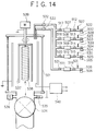
- FIG. 12(A) is a schematic longitudinal sectional view, partly broken away, of an example of the microwave discharging fabrication apparatus which is suitable for the production of a light receiving member for use in electrophographic image reproduction (that is, an electrophotographic image-forming member).
- FIG. 12(B) is a schematic cross sectional view, taken along the line X-X in FIG. 12(A).
- Reference numeral 302 indicates a microwave transmissive window which is hemetically disposed at the end of the cylindrically-shaped portion of the waveguide 303.
- the microwave transmissive window 302 is made of a material capable of allowing a microwave to transmit therethrough such quartz, alumina ceramics, or the like.
- the reaction chamber 301 is provided with an exhaust pipe 304 which is connected through a main valve (not shown) to an exhaust device including diffusion pump, and the like (not shown).
- the reaction chamber 301 is desired to be provided with an exhaust system comprising such exhaust pipe and exhaust device which serves to evacuate the inside thereof and another exhaust system comprising such exhaust pipe and exhaust device which serves to exhaust gases used in the film formation.
- Reference numeral 308 indicates a bias electrode capable of serving also as a gas feed pipe which is longitudinally installed near or in the center of the discharge space 306.
- the bias electrode 308 is electrically connected to an external DC power source 309.
- the bias electrode 308 serves to apply a given bias voltage in order to desirably control the electric potential of a plasma generated in the discharge space 306 upon film formation.
- the bias electrode 308 is made to serve also as the gas feed pipe, it is desired to be designed such that it is provided with a plurality of gas liberation holes (not shown) so as to radiately supply a film-forming raw material gas in the discharge space 306.
- the bias electrode 308 as the gas feed pipe is connected to a gas supply system comprising pipe ways provided with flow controllers (not shown) connected to gas reservoirs (this gas supply system is not shown).
- a gas supply system comprising pipe ways provided with flow controllers (not shown) connected to gas reservoirs (this gas supply system is not shown).
- the reaction chamber 301 it is possible for the reaction chamber 301 to have one or more independent gas feed pipes (not shown) in the reaction chamber 301.
- the independent gas feed pipe is desired to have a plurality of gas liberation holes, and it is connected to the above gas supply system.
- a gas feed pipe is disposed between every adjacent cylindrical substrate holders 307 such that the discharge space 306 is circumscribed by the cylindrical substrate holders 307 and a plurality of gas feed pipes.
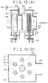
- FIGs. 15(A) and 15(B) Shown in FIGs. 15(A) and 15(B) is of another example of the microwave discharging fabrication apparatus suitable for the production of a light receiving member for use in electrophographic image reproduction (that is, an electrophotographic image-forming member).
- the constitution of the microwave discharging fabrication apparatus shown in FIGs. 15(A) and 15 (B) is of a partial modification of the apparatus shown in FIGs. 12 (A) and 12(B), wherein the shape of the cylindrical reaction chamber of the apparatus shown in FIGs. 12 (A) and 12(B) is changed into a rectangular shape.
- FIG. 15(A) is a schematic longitudinal sectional view, partly broken away, of another example of the microwave discharging fabrication apparatus, and FIG.
- the light receiving member according to the present invention may be produced using any of the apparatus shown in FIGs. 12(A) and 12(B) and FIGs. 15(A) and 15(B) as will be described below.
- a cylindrical substrate 305 is placed on each cylindrical substrate holder 307 in the reaction chamber 301. Then all the cylindrical substrate holders 307 are made rotating by revolving the driving motor 310. Thereafter, the inside of the reaction chamber 301 is evacuated through the exhaust pipe by actuating the diffusion pump (not shown) to thereby bring the discharge space 306 to a vacuum of about 1 x 10 ⁇ 7 Torr or less. The evacuation in this case is desired to be gently conducted at the beginning state in order to prevent foreign matters such as dusts present in the reaction chamber 301 from blowing up to the substrates 305. Then, the electric heater 307' of each substrate holder 307 is energized to heat each cylindrical substrate 307 to a desired temperature.
- a first layer that is, a nc-Si:(H,X) layer
- a first layer that is, a nc-Si:(H,X) layer
- silane gas for example, SiH4, Si2H6, SiF4 or SiH2F2 gas
- a doping gas for example, comprising B2H6 diluted to a desired dilution rate with a given dilution gas such as He gas, and H2 gas or/and halogen gas are introduced into the reaction chamber 301 at predetermined respective flow rates.
- the gas pressure in the reaction chamber 301 is adjusted to a desired vacuum degree by regulating the foregoing main valve of the exhaust pipe.
- the microwave power source (not shown) is switched on to thereby introduce a microwave energy of a desired power (with a frequency of 500 MHz or above, preferably 2.45 GHz) into the discharge space 306 through the waveguide 303 and the microwave transmissive window 302.
- the DC power source 309 is switched on to apply a desired bias voltage into the reaction chamber through the bias electrode 308, wherereby glow discharge is caused in the discharge space 306 to produce a plasma while the potential of said plasma being desirably controlled, wherein the raw material gases are decomposed in the discharge space to produce active species, resulting in causing the formation of a deposited non-single crystal film (specifically, an a-Si:(H,X) film doped with B in this case) on each cylindrical substrate 305.
- a deposited non-single crystal film specifically, an a-Si:(H,X) film doped with B in this case
- B2H6/H2 gas diluted to 3000 ppm with H2 gas
- He gas at 1000 sccm
- a second layer is formed under the conditions of using SiH4 gas at 200 sccm, B2H6/H2 gas (diluted to 3000 ppm) at 10 sccm, and He gas at 2000 sccm
- the flow rates of the three raw material gases used in the formation of the first layer are switched to those flow rates employed in the formation of the second layer, for example, by means of a mass flow controller without suspending the discharge.
- a first nc-Si:(H,X) layer is formed using raw material gases (for example, SiH4 gas, B2H6/H2 gas, gas for supplying hydrogen atoms or halogen atoms, and He gas) and a second nc-Si:(H,X) layer is formed using a carbon atom-supplying raw material gas in addition to the raw material gases used in the formation of the first layer
- the flow rates of the raw material gases used in the formation of the first layer are switched to desired flow rates for the formation of the second layerthe while promptly increasing the flow rate of the carbon atom-supplying gas to a desired value, without suspending the discharge.
- any of the above manners may be employed in the case of controlling the amount of hydrogen atoms or/and halogen atoms contained in the bulk layer region of each adjacent layer.
- the amount of hydrogen atoms or/and halogen atoms contained in the bulk layer region of each adjacent layer it is not always required to be precisely controlled as in the case of forming the interface neighborhood region, and therefore, it is sufficient to be controlled by way of properly adjusting the flow rate of the related raw material gas.
- FIG. 14 is a schematic diagram illustrating the constitution of an example of the RF plasma CVD apparatus suitable for the production of the light receiving member having the foregoing specific multi-layered light receiving layer according to the present invention.
- gas reservoirs 502, 503, 504, 505, and 506 are charged with gaseous raw materials for forming the respective constituent layers in the present invention, that is, for instance, SiH4 gas (99.999% purity) in the gas reservoir 502, B2H6 gas (99.999% purity) diluted with H2 (hereinafter referred to as B2H6/H2 gas) in the gas reservoir 503, CH4 gas (99.999% purity) in the gas reservoir 504, SiF4 gas (99.999% purity) in the reservoir 505, and H2 gas (99.999% purity) in the gas reservoir 506.
- valves 522 through 526 for the gas reservoirs 502 through 506 and a leak valve 535 are closed and that inlet valves 512 through 516, exit valves 517 through 521, and sub-valves 532 and 533 are opened.
- a main valve 534 is at first opened to evacuate the inside of the reaction chamber 501 and gas piping by means of a vacuum pump (not shown). Thereafter, upon observing that the reading on a vacuum gage 536 became about 5 x 10 ⁇ 6 Torr, the sub-valves 532 and 533 and the exit valves 517 through 521 are closed.
- a first nc-Si:(H,X) constituent layer is formed in the following manner. That is, SiH4 gas from the gas reservoir 502, B2H6/H2 gas from the gas reservoir 503, CH4 gas from the gas reservoir 504, and H2 gas from the gas reservoir 506 are caused to flow into mass flow controllers 507, 508, 509, and 511 respectively by opening the valves 522, 523, 524, and 526, controlling the pressure of each of exit pressure gages 527, 528, 529, and 531 is controlled to 1 kg/cm2, and gradually opening the inlet valves 512, 513, 514, and 516.
- the outlet valves 517, 518, 519, and 521 and the sub-valves 532 and 533 are gradually opened to enter the gases into the reaction chamber 501.
- the exit valves 517, 518, 519, and 521 are adjusted so as to attain a desired value for the ratio among the SiH4 gas flow rate, B2H6/H2 gas flow rate, CH4 gas flow rate, and H2 gas flow rate, and the opening of a main valve 534 is adjusted while observing the reading on the vacuum gage 536 so as to attain a desired value for the inner pressure of the reaction chamber 501.
- a RF power source 540 is switched on to apply a desired RF power into the reaction chamber 501 to case glow discharge therein while controlling the flow rates for the SiH4 gas, B2H6/H2 gas, CH4 gas, and H2 gas in accordance with a given variation coefficient curve previously designed by using a microcomputer (not shown), thereby forming, for example, a nc-Si:(H,X) layer containing carbon atoms (C) and boron atoms (B) on the cylinder substrate 537.
- a second nc-Si:(H,X) constituent layer is formed in the following manner. That is, subsequent to the procedures as above described, closing the valves 523, 513, and 518 for the B2H6/H2 gas, SiH4 gas, CH4 gas and H2 gas are entered into the reaction chamber 501 while properly controlling the flow rates for the SiH4 gas, CH4 gas and H2 gas in the same manner as in the above, whereby a nc-Si:(H,X) second layer containing carbon atoms but containing no boron atom is formed on the first layer.
- the inside of the system is once evacuated to a high vacuum degree by closing the exit valves 517 through 521 while opening the sub-valves 532 and 533 and fully opening the main valve 534 for avoiding the gases having been used in the reaction chamber and in the gas pipeways from the exit valves to the inside of the reaction chamber.
- the formation of the second layer may be conducted by switching the flow ratio among the flow rates of the raw material gases employed for the formation of the first layer to a desired flow ratio among the flow rates of the raw material gases for the formation of the second layer.
- the present inventor prepared (a) a plurality of light receiving member samples each comprising a substrate and a two-layered nc-Si:H:X light receiving layer having a layer interface neighborhood region containing hydrogen atoms (H) in a fixed amount and halogen atoms (X) at a different concentration distribution by means of the foregoing microwave plasma CVD technique, (b) a plurality of light receiving member samples each comprising a substrate and a two-layered nc-Si:H:X light receiving layer having a layer interface neighborhood region containing halogen atoms (X) in a fixed amount and hydrogen atoms (H) a different concentration distribution by means of the foregoing microwave plasma CVD technique, and (c) a plurality of light receiving member samples each comprising a substrate and a two-layered nc-Si:H:X light receiving layer having a layer interface neighborhood region containing hydrogen atoms (H) and halogen atoms (X) respectively at a different concentration distribution by means of the
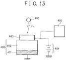
- reference numeral 400 indicates the light receiving member specimen comprising the substrate 401 and the two-layered nc-Si:H:X light receiving layer 402.
- Reference numeral 403 indicates a glass plate having a ITO film as a transparent and conductive electrode formed thereon by means of a conventional vacuum evaporation technique. The glass plate is contacted to the light receiving member specimen 400 through the ITO film side by using a material having a high dielectric constant (glycerin).
- Reference numeral 404 indicates a DC power source which is electrically connected to the ITO film.
- Reference numeral 405 indicates a light source, and reference numeral 406 indicates a conventional TFO (time of flight) measuring device.
- the light receiving member in general, is subjected to corona charging to provide a charge at the surface thereof, followed by subjecting to image exposure to form a latent image on the surface of the light receiving member, and the latent image formed is subjected to development.
- the measurement of photocarrier mobility of the light receiving member during the image-forming process is extremely difficult for the reasons that since the light receiving member is being rotated, the measurement of a surface charge must be conducted under noncontact condition, and in addition to this, the position for the measurement is limited because of the presence of the charger, exposure mechanism, and the like.
- the measurement of photocarrier mobility in this experiment was conducted by establishing pseudoconditions of conducting electrophotographic image-forming process.
- the DC power source 404 was switched on to apply a given voltage between the substrate 401 and the light receiving layer 402 thereby imparting a given surface potential thereto, and a given pulse with short width from the light source 405 was irradiated through the glass 403 to the light receiving member specimen 400, wherein photocurrent was flown in the light receiving member specimen 400, and the value of the photocurrent flown and the period during which the photocurrent was flown were measured by the measuring device 406.
- the light source 405 there was used a dye laser of 460 nm in wavelength excited with N2 laser.
- the irradiation of the pulse with short width was conducted under conditions of 100 to 500 V for the initialization surface potential and 20 nsec for the pulse duration.
- dangling bonds or/and various states are formed within the optical band gap of the neighborhood region of the layer interface, resulting in hindering the transmission of light in the vicinity of the layer interface upon light irradiation to reduce the utilization efficiency of the light, and in deteriorating the properties of the neighborhood region of the layer interface to reduce the efficiency of generating photocarriers (that is, the quantum efficiency).
- a so-called band bending that is, energy band bending
- band bending that is, energy band bending
- the halogen atoms (X) are contained in the neighborhood region of the interface between the adjacent layers at an enhanced concentration distribution, the halogen atoms (X) do not negatively influence to the optical band gap of each non-single crystal adjacent layer, and because of this, a desirable junction is attained at the layer interface between the adjacent layers.
- the hydrogen atoms (H) are contained in the neighborhood region of the interface between the adjacent layers at an enhanced concentration distribution together with the halogen atoms (X), the dangling bonds which are remained without being compensated by the halogen atoms (X) are entirely compensated by the hydrogen atoms (H).
- a light receiving member having a light receiving layer having a stacked structure comprising at least two nc-Si:(H,X) layers each having a different chemical composition
- the content of hydrogen atoms (H) or/and halogen atoms (X) in (i) the neighborhood region of the interface between the adjacent constituent layers or in (ii) the neighborhood region of the interface between the substrate and the light receiving layer is excessive or when any of the neighborhood regions (i) and (ii) containing hydrogen atoms (H) or/and halogen atoms (X) at a relatively higher concentration distribution is excessively extended, not only the layer interface but also any of these interface neighborhood regions are liable to be poor not only in terms of the structural stability but also in terms of the quality.
- Said layer interface neighborhood region in each case comprises a interface neighborhood region 1 situated on the charge injection inhibition layer side and another interface neighborhood region 2 situated on the photoconductive layer side, wherein the sum of the thicknesses of these two layer interface regions is designed to be of a given value in the range of 0.005 to 0.8 ⁇ m.
- the constituent three layers of the three-layered nc-Si light receiving layer of each light receiving member were continuously formed without suspending the discharge under the conditions shown in Table 1, wherein the interface neighborhood region 1 was formed following the procedures of forming the charge injection inhibition layer except for additionally using H2 gas at a given flow rate in the range of 0 to 1 slm and changing each of the inner pressure and bias voltage to a given value in the corresponding range of Table 1, and the interface neighborhood region 2 was formed following the procedures of forming the photoconductive layer except for additionally using H2 gas at a given flow rate in the rang of 0 to 1 slm and changing each of the inner pressure and bias voltage to a given value in the corresponding range of Table 1.
- each light receiving member sample it was cut in the layer thickness direction to obtain a plurality of specimens for evaluation.
- One of these specimens was subjected to analysis of the hydrogen content in each of the charge injection inhibition layer, layer interface neighborhood region and photoconductive layer by means of the secondary ion mass spectrometry (SIMS). Based on the results obtained, it was found that the relative value of the hydrogen content in the layer interface neighborhood region to that in the bulk layer region containing the hydrogen atoms at a relatively higher concentration (that is, the bulk layer region of the charge injection inhibition layer) is in the range of 1.0 to 2.2. And it was also found that the later interface neighborhood region is of a thickness in the range of 50 to 8000 ⁇ .
- a to g to indicate respective light receiving member samples which are different from each other in terms of the thickness of the layer interface neighborhood region, and A1 to A7 illustrate respectively the condition of the H2 gas flow rate employed upon forming the layer interface neighborhood region, wherein A1 indicates the case where the H2 gas flow rate was made to be 0 slm, A2 indicates the case where the H2 gas flow rate was made to be 0.1 slm, A3 indicates the case where the H2 gas flow rate was made to be 0.2 slm, A4 indicates the case where the H2 gas flow rate was made to be 0.4 slm, A5 indicates the case where the H2 gas flow rate was made to be 0.6 slm, A6 indicates the case where the H2 gas flow rate was made to be 0.8 slm, and A7 indicates the case where the H2 gas flow rate was made to be 1.0 slm.
- one of the remaining light receiving member specimens obtained in the above as for each light receiving member sample was subjected to evaluation with respect to photoresponsibility in accordance with the foregoing measuring manner using the measuring system shown in FIG. 13, except for replacing the dye laser as the light source 405 by a halogen lamp.
- light from the halogen lamp as the light source 405 was irradiated to the light receiving member specimen, wherein the photocurrent was measured from the initial stage when the light irradiation started to the stage when the photocurrent became to be of a fixed current value in relation to the lapse of time. Based on the measured results, there was obtained a change of rate in terms of photocurrent value per unit time period. The resultant value was made to be the photoresponsibility of the light receiving member sample involved.
- Example 1 The procedures of Example 1 were repeated, except that the thickness of the charge injection inhibition layer or/and the thickness of the photoconductive layer were thinned to be in the range of 1 to 2 ⁇ m, to thereby obtain various kinds of light receiving member samples each comprising a substrate comprising an aluminum cylinder having a mirror-ground surface and a three-layered non-single crystal silicon (nc-Si) light receiving layer disposed on said mirror-ground surface of the aluminum cylinder as the substrate, said three-layered nc-Si light receiving layer comprising a charge injection inhibition layer, a photoconductive layer and a surface layer being stacked in this order on the substrate, and said three-layered light receiving layer having a different layer interface neighborhood region in terms of the content of hydrogen atoms (H) at the interface between said charge injection inhibition layer and said photoconductive layer.
- nc-Si non-single crystal silicon
- Each light receiving member sample was evaluated with respect to photoresponsibility in the same manner as in Example 1.
- the thickness of the bulk layer region of the charge injection inhibition layer or/and the thickness of the bulk layer region of the photoconductive layer are relatively thin (that is, 1 to 2 ⁇ m thick)
- the layer interface neighborhood region containing the hydrogen atoms at an enhanced concentration distribution is of a thickness corresponding to 30% or less of the thickness of the bulk layer region of the charge injection inhibition layer or the bulk layer region of the photoconductive layer which is thinner, the resulting light receiving member exhibits a significantly improved photoresponsibility.
- Each light receiving member sample was evaluated with respect to photoresponsibility in relation to the hydrogen content in each of the charge injection inhibition layer, the photoconductive layer and the layer interface neighborhood region in the same manner as in Example 1.
- Said layer interface neighborhood region comprises a interface neighborhood region 1 situated on the photoconductive layer side and another interface neighborhood region 2 situated on the surface layer side, wherein the sum of the thicknesses of these two layer interface regions is designed to be of a given value in the range of 0.005 to 0.8 ⁇ m.
- the constituent three layers of the two-layered nc-Si light receiving layer of each light receiving member were continuously formed without suspending the discharge under the conditions shown in Table 4, wherein the interface neighborhood region 1 was formed following the procedures of forming the photoconductive layer except for additionally using H2 gas at a given flow rate in the range of 0 to 1 slm and changing each of the inner pressure and bias voltage to a given value in the corresponding range of Table 4, and the interface neighborhood region 2 was formed following the procedures of forming the surface layer except for additionally using H2 gas at a given flow rate in the range of 0 to 1 slm and changing each of the inner pressure and bias voltage to a given value in the corresponding range of Table 4.
- each kind light receiving member there were prepared six electrophotographic light receiving member samples. In each case, of the six light receiving member samples, one was randomly chosen and subjected to the following evaluations.
- each light receiving member sample it was cut in the layer thickness direction to obtain a plurality of specimens for evaluation.
- One of these specimens was subjected to analysis of the hydrogen content in each of the photoconductive layer, layer interface neighborhood region and surface layer by means of the SIMS.
- Example 4 The procedures of Example 4 were repeated, except that the layer-forming conditions of Table 4 were changed to those shown in Table 5, to thereby obtain various kinds of light receiving member samples each comprising a substrate comprising an aluminum cylinder having a mirror-ground surface and a two-layered non-single crystal silicon (nc-Si) light receiving layer disposed on said mirror-ground surface of the aluminum cylinder as the substrate, said two-layered nc-Si light receiving layer comprising a charge transportation layer and a charge generation layer being stacked in this order on the substrate, and said two-layered light receiving layer having a different layer interface neighborhood region in terms of the content of hydrogen atoms (H) at the interface between said charge transportation layer and said charge generation layer.
- nc-Si non-single crystal silicon
- the thickness of the bulk layer region of the photoconductive layer or/and the thickness of the bulk layer region of the surface layer are relatively thin (that is, 1 to 2 ⁇ m thick)
- the layer interface neighborhood region containing the hydrogen atoms at an enhanced concentration distribution is of a thickness corresponding to 30% or less of the thickness of the bulk layer region of the photoconductive layer or the bulk layer region of the surface layer which is thinner, the resulting light receiving member is significantly excellent especially in terms of photocarrier mobility.
- the resulting light receiving member is significantly excellent especially in terms of photocarrier mobility.
- Each of the light receiving member samples obtained in the above (1) and (2) was evaluated with respect to photocarrier mobility in relation to the hydrogen content in each bulk layer region and the layer interface neighborhood region in the same manner as in Example 4.
- Example 1 The procedures of Example 1 were repeated, except that the layer-forming conditions of Table 1 were changed to those shown in Table 6, to thereby obtain various kinds of light receiving members each comprising a substrate comprising an aluminum cylinder having a mirror-ground surface and a four-layered non-single crystal silicon (nc-Si) light receiving layer disposed on said mirror-ground surface of the aluminum cylinder as the substrate, said four-layered nc-Si light receiving layer comprising a charge injection inhibition layer, a charge transportation layer, a charge generation layer and a surface layer being stacked in this order on the substrate, and said four-layered light receiving layer having a different layer interface neighborhood region in terms of the content of hydrogen atoms (H) at the interface between said charge transportation layer and said charge generation layer.
- nc-Si non-single crystal silicon
- the constituent four layers of the four-layered nc-Si light receiving layer of each light receiving member were continuously formed without suspending the discharge under the conditions shown in Table 6, wherein the interface neighborhood region 1 was formed following the procedures of forming the charge transportation layer except for additionally using H2 gas at a given flow rate in the range of 0 to 1 slm and changing each of the inner pressure and bias voltage to a given value in the corresponding range of Table 6, and the interface neighborhood region 2 was formed following the procedures of forming the charge generation layer except for additionally using H2 gas at a given flow rate in the range of 0 to 1 slm and changing each of the inner pressure and bias voltage to a given value in the corresponding range of Table 6.
- each light receiving member sample it was cut in the layer thickness direction to obtain a plurality of specimens for evaluation.
- One of these specimens was subjected to analysis of the hydrogen content in each of the charge transportation layer, layer interface neighborhood region and charge generation layer by means of the SIMS.
- Example 8 The procedures of Example 8 were repeated, except that the thickness of the charge transportation layer or/and the thickness of the charge generation layer were thinned to be in the range of 1 to 2 ⁇ m, to thereby obtain various kinds of light receiving member samples each comprising a substrate comprising an aluminum cylinder having a mirror-ground surface and a four-layered non-single crystal silicon (nc-Si) light receiving layer disposed on said mirror-ground surface of the aluminum cylinder as the substrate, said four-layered nc-Si light receiving layer comprising a charge injection inhibition layer, a charge transportation layer, a charge generation layer, and a surface layer being stacked in this order on the substrate, and said two-layered light receiving layer having a different layer interface neighborhood region in terms of the content of hydrogen atoms (H) at the interface between said charge transportation layer and said charge generation layer.
- nc-Si non-single crystal silicon
- the thickness of the bulk layer region of the charge transportation layer or/and the thickness of the bulk layer region of the charge generation layer are relatively thin (that is, 1 to 2 ⁇ m thick)
- the layer interface neighborhood region containing the hydrogen atoms at an enhanced concentration distribution is of a thickness corresponding to 30% or less of the thickness of the bulk layer region of the charge transportation layer or the bulk layer region of the charge generation layer which is thinner, the resulting light receiving member is significantly excellent especially in terms of photocarrier mobility.
- Example 8 The procedures of Example 8 were repeated, except that the amount of the hydrogen atoms incorporated into not only the bulk layer region of each of the charge transportation layer and the charge generation layer but also the layer interface neighborhood region was varied, to thereby obtain various kinds of light receiving member samples each comprising a substrate comprising an aluminum cylinder having a mirror-ground surface and a four-layered non-single crystal silicon (nc-Si) light receiving layer disposed on said mirror-ground surface of the aluminum cylinder as the substrate, said four-layered nc-Si light receiving layer comprising a charge injection inhibition layer, a charge transportation layer having a different hydrogen content, a charge generation layer having a different hydrogen content, and a surface layer being stacked in this order on the substrate, and said four-layered light receiving layer having a different layer interface neighborhood region in terms of the content of hydrogen atoms (H) at the interface between said charge transportation layer and said charge generation layer.
- nc-Si non-single crystal silicon
- Each of the light receiving member samples obtained in the above was evaluated with respect to photocarrier mobility in relation to the hydrogen content in each bulk layer region and the layer interface neighborhood region in the same manner as in Example 4.
- Example 11 The procedures of the foregoing Example 11 were repeated, except that no layer interface neighborhood region was formed, to thereby obtain six comparative light receiving member samples each having a two-layered nc-Si light receiving layer comprising a charge injection inhibition layer and a photoconductive layer.
- Example 15 As for each of the light receiving member samples obtained in Example 15 and Comparative Examples 4 and 5, evaluation was made with respect to charge retentivity, photosensitivity, residual potential, and appearance of uneven density image (or halftone reproduction). The evaluation of each of the charge retentivity, photosensitivity, and appearance of uneven density image (or halftone reproduction) was conducted in the same evaluation manner as in Example 1, wherein the evaluation as for each of the these evaluation items was conducted after 500,000 times repeated shots in the case where the image-forming process was conducted at ordinary process speed (A) and also in the case where the image-forming process was conducted at a process speed (B) which is higher as much as 1.2 holds over the process speed (A).
- the evaluation of the residual potential was conducted in the following manner. That is, the light receiving member sample is set to the foregoing electrophotographic copying machine modified for experimental purposes, wherein the light receiving member sample is charged so as to provide a given surface potential in dark therefor, soon after this, a given quantity of relatively intense light from a Xenon lamp is irradiated thereto while excluding light of less than 550 nm by means of a cut-filter, wherein the surface potential in light of the light receiving member sample is measured by means of an electrostatic voltmeter.
- the surface potential in light obtained in this case is made to be a residual potential of the light receiving member sample. Particularly, the electric potential remained without being attenuated when a given quantity of light is irradiated is evaluated as the residual potential.
- Example 17 The procedures of Example 17 were repeated, except that no layer interface neighborhood region was formed, to thereby obtain six comparative light receiving member samples each having a four-layered nc-Si light receiving layer comprising a charge injection inhibition layer, a charge transportation layer, a charge generation layer and a surface layer.
- the light receiving member sample is set to the foregoing electrophotographic copying machine modified for experimental purposes, wherein a given surface portion of the light receiving member sample which is corresponding to the space between successively feeding papers is charged so as to provide a given surface potential in dark therefor under the condition that no blank exposure light is irradiated.
- a surface potential in dark in the circumferential direction of the light receiving member sample in this case is measured by means of an electrostatic voltmeter and the measured result (Data 1) obtained is memorized in a computer.
- the light receiving member sample is one which is accompanied by a photomemory
- the history based on the irradiation of blank exposure light is remained on the portion of light receiving member sample having been irradiated with blank exposure light to cause a difference in terms of the surface potential in dark between the Data 1 and 2.
- the evaluation of photomemory is conducted based on the magnitude of this difference. In order to precisely measure the difference in terms of the surface potential in dark by overlapping the Data 1 and 2, the measuring timing is adjusted so that each measurement may be conducted for the same portion of the light receiving member sample.
- the evaluation is conducted after 500,000 times repeated shots in the case where the image-forming process is conducted at ordinary process speed (A) and also in the case where the image-forming process is conducted at a process speed (B) which is higher as much as 1.2 holds over the process speed (A).
- each light receiving member sample comprises six samples, this evaluation is conducted for all of them. And one which is worst in terms of photomemory is dedicated for the evaluation on the following criteria.
- o the case wherein the result is excellent
- ⁇ the case wherein the result is good
- ⁇ the case wherein the result is not so good but practically acceptable
- X the case wherein the result is inferior but seems practically acceptable.
- Said layer interface neighborhood region in each case comprises a interface neighborhood region 1 situated on the charge injection inhibition layer side and another interface neighborhood region 2 situated on the photoconductive layer side, wherein the sum of the thicknesses of these two layer interface regions is designed to be of a given value in the range of 0.005 (50 ⁇ ) to 2 ⁇ m, and the amount of the halogen atoms (X) is varied in the range of 0.1 atomic ppm to 35 atomic% in terms of the ratio to the amount of the total constituent atoms thereof.
- each kind light receiving member there were prepared six electrophotographic light receiving member samples. In each case, of the six light receiving member samples, one was randomly chosen and subjected to the following evaluations.
- each light receiving member sample it was cut in the layer thickness direction to obtain a plurality of specimens for evaluation.
- One of these specimens was subjected to analysis of the halogen content in the layer interface neighborhood region by means of the SIMS. The results obtained are collectively shown in Table 14.
- one of the remaining light receiving member specimens obtained in the above as for each light receiving member sample was subjected to evaluation with respect to photocarrier mobility ( ⁇ ) in accordance with the foregoing photocarrier mobility measuring manner using the measuring system shown in FIG. 13.
- Each of the light receiving members obtained in the above (1), (2) and (3) was evaluated with respect to photocarrier mobility in relation to the halogen content of the layer interface neighborhood region in the same manner as in Example 21.
- the resulting light receiving member exhibits a significantly improved photocarrier mobility.
- Example 24 The procedures of Example 24 were repeated, except that the conditions shown in Table 18 was replaced by the conditions shown in Table 21, to thereby obtain six light receiving member samples each comprising a substrate comprising an aluminum cylinder having a mirror-ground surface and a three-layered non-single crystal silicon (nc-Si) light receiving layer disposed on said mirror-ground surface of the aluminum cylinder as the substrate, said three-layered nc-Si light receiving layer comprising a charge injection inhibition layer, a photoconductive layer and a suface layer being stacked in this order on the substrate, and said three-layered light receiving layer having a 5000 ⁇ thick layer interface neighborhood region containing halogen atoms (X) at an enhanced concentration distribution of 1 atomic% in terms of the ratio of the amount of the halogen atoms (X) to that of the total constituent atoms at the interface between said charge injection inhibition layer and said photoconductive layer.
- nc-Si non-single crystal silicon
- Example 24 The procedures of Example 24 were repeated, except that the conditions shown in Table 18 was replaced by the conditions shown in Table 22, to thereby obtain six light receiving member samples each comprising a substrate comprising an aluminum cylinder having a mirror-ground surface and a four-layered non-single crystal silicon (nc-Si) light receiving layer disposed on said mirror-ground surface of the aluminum cylinder as the substrate, said four-layered nc-Si light receiving layer comprising an IR absorption layer, a charge injection inhibition layer, a photoconductive layer and a suface layer being stacked in this order on the substrate, and said four-layered light receiving layer having a 5000 ⁇ thick layer interface neighborhood region containing halogen atoms (X) at an enhanced concentration distribution of 1 atomic% in terms of the ratio of the amount of the halogen atoms (X) to that of the total constituent atoms at the interface between said charge injection inhibition layer and said photoconductive layer.
- nc-Si non-single crystal silicon
- Example 24 The procedures of Example 24 were repeated, except that the conditions shown in Table 18 was replaced by the conditions shown in Table 23, to thereby obtain six light receiving member samples each comprising a substrate comprising an aluminum cylinder having a mirror-ground surface and a four-layered non-single crystal silicon (nc-Si) light receiving layer disposed on said mirror-ground surface of the aluminum cylinder as the substrate, said four-layered nc-Si light receiving layer comprising a charge injection inhibition layer, a charge transportation layer, a charge generation layer and a suface layer being stacked in this order on the substrate, and said four-layered light receiving layer having a 5000 ⁇ thick layer interface neighborhood region containing halogen atoms (X) at an enhanced concentration distribution of 1 atomic% in terms of the ratio of the amount of the halogen atoms (X) to that of the total constituent atoms at the interface between said charge transportation layer and said charge generation layer.
- nc-Si non-single crystal silicon
- Example 24 The procedures of Example 24 were repeated, except that no layer interface layer region was formed, to thereby obtain six light receiving member samples each comprising a substrate comprising an aluminum cylinder having a mirror-ground surface and a two-layered non-single crystal silicon (nc-Si) light receiving layer disposed on said mirror-ground surface of the aluminum cylinder as the substrate, said two-layered nc-Si light receiving layer comprising a charge injection inhibition layer and a photoconductive layer being stacked in this order on the substrate.
- nc-Si non-single crystal silicon
- Example 26 The procedures of Example 26 were repeated, except that no layer interface layer region was formed, to thereby obtain six light receiving member samples each comprising a substrate comprising an aluminum cylinder having a mirror-ground surface and a three-layered non-single crystal silicon (nc-Si) light receiving layer disposed on said mirror-ground surface of the aluminum cylinder as the substrate, said three-layered nc-Si light receiving layer comprising a charge injection inhibition layer, a photoconductive layer and a surface layer being stacked in this order on the substrate.
- nc-Si non-single crystal silicon
- Example 27 The procedures of Example 27 were repeated, except that no layer interface layer region was formed, to thereby obtain six light receiving member samples each comprising a substrate comprising an aluminum cylinder having a mirror-ground surface and a four-layered non-single crystal silicon (nc-Si) light receiving layer disposed on said mirror-ground surface of the aluminum cylinder as the substrate, said four-layered nc-Si light receiving layer comprising an IR absorption layer, a charge injection inhibition layer, a photoconductive layer and a surface layer being stacked in this order on the substrate.
- nc-Si non-single crystal silicon
- Example 28 The procedures of Example 28 were repeated, except that no layer interface layer region was formed, to thereby obtain six light receiving member samples each comprising a substrate comprising an aluminum cylinder having a mirror-ground surface and a four-layered non-single crystal silicon (nc-Si) light receiving layer disposed on said mirror-ground surface of the aluminum cylinder as the substrate, said four-layered nc-Si light receiving layer comprising a charge injection inhibition layer, a charge transportation layer, a charge generation layer and a surface layer being stacked in this order on the substrate.
- nc-Si non-single crystal silicon
- the neighborhood region of the free surface of the outermost layer was designed to contain halogen atoms (X) at an enhanced concentration distribution, to thereby a plurality of light receiving member samples in each case.
- the light receiving member samples obtained were evaluated in the same manner as in Example 24. As a result, satisfactory results were obtained in terms of the electrophotographic characteristics required especially in the case of conducting the image-forming process at an improved, high speed.
- the light receiving member samples obtained were evaluated in the same manner as in Example 24. As a result, satisfactory results were obtained in terms of the electrophotographic characteristics required especially in the case of conducting the image-forming process at an improved, high speed.
- Said layer interface neighborhood region in each case comprises a interface neighborhood region 1 situated on the charge injection inhibition layer side and another interface neighborhood region 2 situated on the photoconductive layer side.
- the constituent two layers of the two-layered nc-Si light receiving layer of each light receiving member were continuously formed without suspending the discharge under the conditions shown in Table 24, wherein the interface neighborhood region 1 was formed following the procedures of forming the charge injection inhibition layer except for additionally using H2 gas at a given flow rate in the range of 0 to 1 slm and SiF4 gas at a given flow rate in the range of 0 to 400 sccm and changing each of the inner pressure and bias voltage to a given value in the corresponding range of Table 24, and the interface neighborhood region 2 was formed following the procedures of forming the photoconductive layer except for additionally using H2 gas at a given flow rate in the range of 0 to 1 slm and SiF4 gas at a given flow rate in the range of 0 to 400 sccm and changing each of the inner pressure and bias voltage to a given value in the corresponding range of Table 24.
- each kind light receiving member there were prepared six electrophotographic light receiving member samples. In each case, of the six light receiving member samples, one was randomly chosen and subjected to the following evaluations.
- each light receiving member sample it was cut in the layer thickness direction to obtain a plurality of specimens for evaluation.
- One of these specimens was subjected to analysis of the hydrogen content and the halogen content in the layer interface neighborhood region by means of the SIMS.
- the resultant light receiving member samples have respectively such a layer interface neighborhood region that the sum of the thicknesses of these two layer interface neighborhood regions containing the halogen atoms (X) (specifically, fluorine atoms) is of a value in the range of 0.005 ⁇ m (50 ⁇ ) to 2 ⁇ m and the ratio of the content of the halogen atoms (X) to that of the total constituent atoms is in the range of 0.1 atomic ppm to 35 atomic ppm and that the sum of the thicknesses of the two layer interface neighborhood regions containing the hydrogen atoms (H) is of a value in the range of 50 to 8000 ⁇ and the hydrogen content thereof is a value of as much as 1.2 to 2.2 holds over that of the adjacent bulk layer region which is relatively greater in terms of the hydrogen content (specifically, the bulk layer region of the charge injection inhibition layer).
- X halogen atoms
- one of the remaining light receiving member specimens obtained in the above as for each light receiving member sample was subjected to evaluation with respect to photocarrier mobility ( ⁇ ) in accordance with the foregoing photocarrier mobility measuring manner using the measuring system shown in FIG. 13.
- Said layer interface neighborhood region in each case comprises a interface neighborhood region 1 situated on the charge transportation layer side and another interface neighborhood region 2 situated on the charge generation layer side.
- the constituent three layers of the three-layered nc-Si light receiving layer of each light receiving member were continuously formed without suspending the discharge under the conditions shown in Table 28, wherein the interface neighborhood region 1 was formed following the procedures of forming the charge transportation layer except for additionally using H2 gas at a given flow rate in the range of 0 to 1 slm and SiF4 gas at a given flow rate in the range of 0 to 400 sccm and changing each of the inner pressure and bias voltage to a given value in the corresponding range of Table 28, and the interface neighborhood region 2 was formed following the procedures of forming the charge generation layer except for additionally using H2 gas at a given flow rate in the range of 0 to 1 slm and SiF4 gas at a given flow rate in the range of 0 to 400 sccm and changing each of the inner pressure and bias voltage to a given value in the corresponding range of Table 28.
- Each of the light receiving members obtained in the above (1) and (2) was evaluated with respect to photocarrier mobility in relation to the hydrogen content and the halogen content of the layer interface neighborhood region in the same manner as in Example 34. As a result, it was found that the evaluated results are substantially the same as those obtained in Example 34.
- Each of the light receiving members obtained in the above (1), (2) and (3) was evaluated with respect to photocarrier mobility in relation to the hydrogen content and the halogen content in the layer interface neighborhood region in the same manner as in Example 34.
- the resulting light receiving member exhibits a significantly improved photocarrier mobility.
- evaluation was made with respect to electrophotographic characteristics including (i) photosensitivity, (ii) charge retentivity, (iii) residual potential, (iv) appearance of faint image, (v) appearance of white spots, (vi) appearance of smeared image, (vii) appearance of ghost, and (viii) halftone reproduction, respectively.
- the evaluation of each of these evaluation items (i) to (viii) was conducted using the foregoing electrophotographic copying machine, modified for experimental purposes, wherein the evaluation was conducted at the stage after 500,000 times repeated shots in the case where the image-forming process was conducted at ordinary process speed and also in the case where the image-forming process was conducted at a process speed which is higher as much as 1.2 holds over the ordinary process speed.
- the light receiving member sample comprises six samples, this evaluation conducted for all of them. An one which is worst in terms of the appearance of faint image is dedicated for the observation on the following criteria: o : the case wherein the copied image is excellent in quality, ⁇ : the case wherein the copied image is good in quality, ⁇ : the case wherein the copied image is not so good in quality but is practically acceptable, and X : the case wherein the copied image is inferior in quality but is practically acceptable.
Landscapes
- Chemical & Material Sciences (AREA)
- Inorganic Chemistry (AREA)
- Physics & Mathematics (AREA)
- General Physics & Mathematics (AREA)
- Photoreceptors In Electrophotography (AREA)
Applications Claiming Priority (12)
| Application Number | Priority Date | Filing Date | Title |
|---|---|---|---|
| JP33322092 | 1992-12-14 | ||
| JP33322092 | 1992-12-14 | ||
| JP333220/92 | 1992-12-14 | ||
| JP96038/93 | 1993-04-22 | ||
| JP96039/93 | 1993-04-22 | ||
| JP9603993 | 1993-04-22 | ||
| JP9603993 | 1993-04-22 | ||
| JP9603893 | 1993-04-22 | ||
| JP9603893 | 1993-04-22 | ||
| JP290561/93 | 1993-11-19 | ||
| JP29056193 | 1993-11-19 | ||
| JP29056193 | 1993-11-19 |
Publications (2)
| Publication Number | Publication Date |
|---|---|
| EP0605972A1 true EP0605972A1 (fr) | 1994-07-13 |
| EP0605972B1 EP0605972B1 (fr) | 1999-10-27 |
Family
ID=27468386
Family Applications (1)
| Application Number | Title | Priority Date | Filing Date |
|---|---|---|---|
| EP93310038A Expired - Lifetime EP0605972B1 (fr) | 1992-12-14 | 1993-12-13 | Elément récepteur de lumière ayant une couche réceptrice de lumière à structure multiple avec une concentration améliorée en atomes d'hydrogène ou/et d'halogène à proximité de l'interface des couches adjacentes |
Country Status (3)
| Country | Link |
|---|---|
| US (1) | US5514506A (fr) |
| EP (1) | EP0605972B1 (fr) |
| DE (1) | DE69326878T2 (fr) |
Families Citing this family (12)
| Publication number | Priority date | Publication date | Assignee | Title |
|---|---|---|---|---|
| JP3530676B2 (ja) | 1995-04-26 | 2004-05-24 | キヤノン株式会社 | 光受容部材の製造方法、該光受容部材、該光受容部材を有する電子写真装置及び該光受容部材を用いた電子写真プロセス |
| JP3368109B2 (ja) * | 1995-08-23 | 2003-01-20 | キヤノン株式会社 | 電子写真用光受容部材 |
| JPH1165146A (ja) | 1997-08-22 | 1999-03-05 | Canon Inc | 電子写真用光受容部材 |
| US6406824B1 (en) | 1998-11-27 | 2002-06-18 | Canon Kabushiki Kaisha | Electrophotographic photosensitive member and electrophotographic apparatus having the photosensitive member |
| US6936389B2 (en) * | 2000-07-17 | 2005-08-30 | Bridgestone Corporation | Base body for photosensitive drum and photosensitive drum |
| JP2004014812A (ja) * | 2002-06-07 | 2004-01-15 | Canon Inc | 光起電力素子 |
| KR100950133B1 (ko) * | 2002-12-27 | 2010-03-30 | 엘지디스플레이 주식회사 | 인쇄방식에 의한 패턴형성방법 |
| JP4171428B2 (ja) * | 2003-03-20 | 2008-10-22 | 三洋電機株式会社 | 光起電力装置 |
| JP2005062846A (ja) * | 2003-07-31 | 2005-03-10 | Canon Inc | 電子写真感光体 |
| EP1643564B1 (fr) * | 2004-09-29 | 2019-01-16 | Panasonic Intellectual Property Management Co., Ltd. | Dispositif photovoltaique |
| JP4939176B2 (ja) * | 2005-12-22 | 2012-05-23 | キヤノン株式会社 | 有機el素子 |
| CA2757789A1 (fr) * | 2008-10-30 | 2010-05-06 | Gvbb Holdings S.A.R.L. | Appareil, procede et programme de codage d'images |
Citations (5)
| Publication number | Priority date | Publication date | Assignee | Title |
|---|---|---|---|---|
| DE3346891A1 (de) * | 1982-12-27 | 1984-06-28 | Canon K.K., Tokio/Tokyo | Fotoleitfaehiges aufzeichnungselement |
| JPS59119360A (ja) * | 1982-12-27 | 1984-07-10 | Canon Inc | 電子写真用光導電部材 |
| US4722880A (en) * | 1984-10-03 | 1988-02-02 | Matsushita Electric Industrial Co., Ltd. | Photoconductor having amorphous silicon hydride |
| US4882251A (en) * | 1987-04-22 | 1989-11-21 | Canon Kabushiki Kaisha | Light receiving member having a multilayered light receiving layer composed of a lower layer made of aluminum-containing inorganic material and an upper layer made of non-single-crystal silicon material |
| US4886723A (en) * | 1987-04-21 | 1989-12-12 | Canon Kabushiki Kaisha | Light receiving member having a multilayered light receiving layer composed of a lower layer made of aluminum-containing inorganic material and an upper layer made of non-single-crystal silicon material |
Family Cites Families (11)
| Publication number | Priority date | Publication date | Assignee | Title |
|---|---|---|---|---|
| DE2746967C2 (de) * | 1977-10-19 | 1981-09-24 | Siemens AG, 1000 Berlin und 8000 München | Elektrofotographische Aufzeichnungstrommel |
| US4265991A (en) * | 1977-12-22 | 1981-05-05 | Canon Kabushiki Kaisha | Electrophotographic photosensitive member and process for production thereof |
| GB2018446B (en) * | 1978-03-03 | 1983-02-23 | Canon Kk | Image-forming member for electrophotography |
| FR2433871A1 (fr) * | 1978-08-18 | 1980-03-14 | Hitachi Ltd | Dispositif de formation d'image a semi-conducteur |
| JPS574172A (en) * | 1980-06-09 | 1982-01-09 | Canon Inc | Light conductive member |
| JPS574053A (en) * | 1980-06-09 | 1982-01-09 | Canon Inc | Photoconductive member |
| US4394425A (en) * | 1980-09-12 | 1983-07-19 | Canon Kabushiki Kaisha | Photoconductive member with α-Si(C) barrier layer |
| US4394426A (en) * | 1980-09-25 | 1983-07-19 | Canon Kabushiki Kaisha | Photoconductive member with α-Si(N) barrier layer |
| JPS59113447A (ja) * | 1982-12-20 | 1984-06-30 | Canon Inc | 電子写真用光導電部材 |
| US4906542A (en) * | 1987-04-23 | 1990-03-06 | Canon Kabushiki Kaisha | Light receiving member having a multilayered light receiving layer composed of a lower layer made of aluminum-containing inorganic material and an upper layer made of non-single-crystal silicon material |
| US4986574A (en) * | 1990-01-11 | 1991-01-22 | Fisher Controls International, Inc. | Raised face flange alignment tool |
-
1993
- 1993-12-13 DE DE69326878T patent/DE69326878T2/de not_active Expired - Lifetime
- 1993-12-13 EP EP93310038A patent/EP0605972B1/fr not_active Expired - Lifetime
- 1993-12-14 US US08/165,840 patent/US5514506A/en not_active Expired - Lifetime
Patent Citations (5)
| Publication number | Priority date | Publication date | Assignee | Title |
|---|---|---|---|---|
| DE3346891A1 (de) * | 1982-12-27 | 1984-06-28 | Canon K.K., Tokio/Tokyo | Fotoleitfaehiges aufzeichnungselement |
| JPS59119360A (ja) * | 1982-12-27 | 1984-07-10 | Canon Inc | 電子写真用光導電部材 |
| US4722880A (en) * | 1984-10-03 | 1988-02-02 | Matsushita Electric Industrial Co., Ltd. | Photoconductor having amorphous silicon hydride |
| US4886723A (en) * | 1987-04-21 | 1989-12-12 | Canon Kabushiki Kaisha | Light receiving member having a multilayered light receiving layer composed of a lower layer made of aluminum-containing inorganic material and an upper layer made of non-single-crystal silicon material |
| US4882251A (en) * | 1987-04-22 | 1989-11-21 | Canon Kabushiki Kaisha | Light receiving member having a multilayered light receiving layer composed of a lower layer made of aluminum-containing inorganic material and an upper layer made of non-single-crystal silicon material |
Non-Patent Citations (2)
| Title |
|---|
| CHAMBOULEYRON ET AL.: "HYDROGEN CONTENT, TRANSPORT PROPERITIES AND LIGHT DEGRATION OF a-Si:H FILMS CONTAINING ARTIFICIALLY GENERATED INTERFACES", SOLAR ENERGY MATERIALS, vol. 17, no. 1, January 1988 (1988-01-01), AMSTERDAM, pages 1 - 16, XP000050975 * |
| PATENT ABSTRACTS OF JAPAN vol. 8, no. 245 (P - 312) 10 November 1984 (1984-11-10) * |
Also Published As
| Publication number | Publication date |
|---|---|
| DE69326878D1 (de) | 1999-12-02 |
| EP0605972B1 (fr) | 1999-10-27 |
| DE69326878T2 (de) | 2000-04-27 |
| US5514506A (en) | 1996-05-07 |
Similar Documents
| Publication | Publication Date | Title |
|---|---|---|
| EP0605972B1 (fr) | Elément récepteur de lumière ayant une couche réceptrice de lumière à structure multiple avec une concentration améliorée en atomes d'hydrogène ou/et d'halogène à proximité de l'interface des couches adjacentes | |
| EP0242231B1 (fr) | Elément photorécepteur ayant des capacités de formation d'images améliorées | |
| JP3368109B2 (ja) | 電子写真用光受容部材 | |
| EP0169641B1 (fr) | Elément photorécepteur | |
| US4595644A (en) | Photoconductive member of A-Si(Ge) with nonuniformly distributed nitrogen | |
| JP3181165B2 (ja) | 光受容部材 | |
| US5741615A (en) | Light receiving member with non-single-crystal silicon layer containing Cr, Fe, Na, Ni and Mg | |
| US4911998A (en) | Process of electrophotographic imaging with layered light receiving member containing A-Si and Ge | |
| EP0809153B1 (fr) | Elément photorécepteur | |
| US5945241A (en) | Light receiving member for electrophotography and fabrication process thereof | |
| US4824749A (en) | Light receiving member for use in electrophotography and process for the production thereof | |
| US6294299B2 (en) | Electrophotographic light-receiving member | |
| JP3862334B2 (ja) | 電子写真用光受容部材 | |
| JP3606395B2 (ja) | 電子写真用光受容部材 | |
| JP3234697B2 (ja) | 光受容部材 | |
| EP0165743B1 (fr) | Elément récepteur de lumière | |
| JP2000171995A (ja) | 電子写真用光受容部材 | |
| JP2824166B2 (ja) | 光受容部材 | |
| JPH09297421A (ja) | 電子写真用光受容部材 | |
| HK1004690B (en) | Light receiving member | |
| JP2002311614A (ja) | 電子写真用光受容部材 | |
| JP2001337472A (ja) | 電子写真感光体、プロセスカートリッジ及び電子写真装置 | |
| JPH11194516A (ja) | 電子写真用光受容部材 | |
| JPH08179532A (ja) | 光受容部材と電子写真用光受容部材 | |
| JPH08179533A (ja) | 光受容部材と電子写真用光受容部材 |
Legal Events
| Date | Code | Title | Description |
|---|---|---|---|
| PUAI | Public reference made under article 153(3) epc to a published international application that has entered the european phase |
Free format text: ORIGINAL CODE: 0009012 |
|
| AK | Designated contracting states |
Kind code of ref document: A1 Designated state(s): DE ES FR GB IT NL |
|
| 17P | Request for examination filed |
Effective date: 19941124 |
|
| 17Q | First examination report despatched |
Effective date: 19960802 |
|
| GRAG | Despatch of communication of intention to grant |
Free format text: ORIGINAL CODE: EPIDOS AGRA |
|
| GRAG | Despatch of communication of intention to grant |
Free format text: ORIGINAL CODE: EPIDOS AGRA |
|
| GRAH | Despatch of communication of intention to grant a patent |
Free format text: ORIGINAL CODE: EPIDOS IGRA |
|
| GRAH | Despatch of communication of intention to grant a patent |
Free format text: ORIGINAL CODE: EPIDOS IGRA |
|
| GRAA | (expected) grant |
Free format text: ORIGINAL CODE: 0009210 |
|
| AK | Designated contracting states |
Kind code of ref document: B1 Designated state(s): DE ES FR GB IT NL |
|
| PG25 | Lapsed in a contracting state [announced via postgrant information from national office to epo] |
Ref country code: NL Free format text: LAPSE BECAUSE OF FAILURE TO SUBMIT A TRANSLATION OF THE DESCRIPTION OR TO PAY THE FEE WITHIN THE PRESCRIBED TIME-LIMIT Effective date: 19991027 Ref country code: ES Free format text: THE PATENT HAS BEEN ANNULLED BY A DECISION OF A NATIONAL AUTHORITY Effective date: 19991027 |
|
| REF | Corresponds to: |
Ref document number: 69326878 Country of ref document: DE Date of ref document: 19991202 |
|
| ET | Fr: translation filed | ||
| ITF | It: translation for a ep patent filed | ||
| NLV1 | Nl: lapsed or annulled due to failure to fulfill the requirements of art. 29p and 29m of the patents act | ||
| PLBE | No opposition filed within time limit |
Free format text: ORIGINAL CODE: 0009261 |
|
| STAA | Information on the status of an ep patent application or granted ep patent |
Free format text: STATUS: NO OPPOSITION FILED WITHIN TIME LIMIT |
|
| 26N | No opposition filed | ||
| REG | Reference to a national code |
Ref country code: GB Ref legal event code: IF02 |
|
| PGFP | Annual fee paid to national office [announced via postgrant information from national office to epo] |
Ref country code: IT Payment date: 20101217 Year of fee payment: 18 Ref country code: GB Payment date: 20101223 Year of fee payment: 18 |
|
| PGFP | Annual fee paid to national office [announced via postgrant information from national office to epo] |
Ref country code: DE Payment date: 20101231 Year of fee payment: 18 |
|
| PGFP | Annual fee paid to national office [announced via postgrant information from national office to epo] |
Ref country code: FR Payment date: 20120103 Year of fee payment: 19 |
|
| GBPC | Gb: european patent ceased through non-payment of renewal fee |
Effective date: 20121213 |
|
| REG | Reference to a national code |
Ref country code: FR Ref legal event code: ST Effective date: 20130830 |
|
| REG | Reference to a national code |
Ref country code: DE Ref legal event code: R119 Ref document number: 69326878 Country of ref document: DE Effective date: 20130702 |
|
| PG25 | Lapsed in a contracting state [announced via postgrant information from national office to epo] |
Ref country code: DE Free format text: LAPSE BECAUSE OF NON-PAYMENT OF DUE FEES Effective date: 20130702 |
|
| PG25 | Lapsed in a contracting state [announced via postgrant information from national office to epo] |
Ref country code: FR Free format text: LAPSE BECAUSE OF NON-PAYMENT OF DUE FEES Effective date: 20130102 Ref country code: GB Free format text: LAPSE BECAUSE OF NON-PAYMENT OF DUE FEES Effective date: 20121213 |
|
| PG25 | Lapsed in a contracting state [announced via postgrant information from national office to epo] |
Ref country code: IT Free format text: LAPSE BECAUSE OF NON-PAYMENT OF DUE FEES Effective date: 20121213 |