EP0606750B1 - Structure magnétique en couches pour utilisation dans une tête magnétique - Google Patents
Structure magnétique en couches pour utilisation dans une tête magnétique Download PDFInfo
- Publication number
- EP0606750B1 EP0606750B1 EP93310325A EP93310325A EP0606750B1 EP 0606750 B1 EP0606750 B1 EP 0606750B1 EP 93310325 A EP93310325 A EP 93310325A EP 93310325 A EP93310325 A EP 93310325A EP 0606750 B1 EP0606750 B1 EP 0606750B1
- Authority
- EP
- European Patent Office
- Prior art keywords
- magnetic
- layer
- composition
- doped
- alloy
- Prior art date
- Legal status (The legal status is an assumption and is not a legal conclusion. Google has not performed a legal analysis and makes no representation as to the accuracy of the status listed.)
- Expired - Lifetime
Links
- 239000010410 layer Substances 0.000 claims description 230
- 229910000702 sendust Inorganic materials 0.000 claims description 143
- 239000000203 mixture Substances 0.000 claims description 96
- 239000000956 alloy Substances 0.000 claims description 50
- 229910045601 alloy Inorganic materials 0.000 claims description 48
- 230000001939 inductive effect Effects 0.000 claims description 24
- 239000007789 gas Substances 0.000 claims description 20
- XEEYBQQBJWHFJM-UHFFFAOYSA-N iron Substances [Fe] XEEYBQQBJWHFJM-UHFFFAOYSA-N 0.000 claims description 19
- 238000000034 method Methods 0.000 claims description 18
- 238000003860 storage Methods 0.000 claims description 17
- 239000002356 single layer Substances 0.000 claims description 8
- 239000004020 conductor Substances 0.000 claims description 7
- IJGRMHOSHXDMSA-UHFFFAOYSA-N Atomic nitrogen Chemical compound N#N IJGRMHOSHXDMSA-UHFFFAOYSA-N 0.000 claims description 6
- 239000000696 magnetic material Substances 0.000 claims description 6
- -1 silicon-aluminium-iron Chemical compound 0.000 claims description 5
- QVGXLLKOCUKJST-UHFFFAOYSA-N atomic oxygen Chemical compound [O] QVGXLLKOCUKJST-UHFFFAOYSA-N 0.000 claims description 3
- 239000001301 oxygen Substances 0.000 claims description 3
- 229910052760 oxygen Inorganic materials 0.000 claims description 3
- XLYOFNOQVPJJNP-UHFFFAOYSA-N water Chemical compound O XLYOFNOQVPJJNP-UHFFFAOYSA-N 0.000 claims 6
- 239000012777 electrically insulating material Substances 0.000 claims 4
- 239000007779 soft material Substances 0.000 claims 2
- 239000010408 film Substances 0.000 description 72
- 239000000463 material Substances 0.000 description 22
- 239000010409 thin film Substances 0.000 description 12
- 239000000758 substrate Substances 0.000 description 9
- 238000000151 deposition Methods 0.000 description 8
- 230000008021 deposition Effects 0.000 description 8
- PNEYBMLMFCGWSK-UHFFFAOYSA-N aluminium oxide Inorganic materials [O-2].[O-2].[O-2].[Al+3].[Al+3] PNEYBMLMFCGWSK-UHFFFAOYSA-N 0.000 description 7
- 230000008569 process Effects 0.000 description 7
- 230000035699 permeability Effects 0.000 description 6
- 238000004544 sputter deposition Methods 0.000 description 6
- 230000001965 increasing effect Effects 0.000 description 5
- 230000006698 induction Effects 0.000 description 5
- 229910000889 permalloy Inorganic materials 0.000 description 5
- XKRFYHLGVUSROY-UHFFFAOYSA-N Argon Chemical compound [Ar] XKRFYHLGVUSROY-UHFFFAOYSA-N 0.000 description 4
- 229910001030 Iron–nickel alloy Inorganic materials 0.000 description 4
- 230000006872 improvement Effects 0.000 description 4
- 238000005137 deposition process Methods 0.000 description 3
- 230000005415 magnetization Effects 0.000 description 3
- 239000000725 suspension Substances 0.000 description 3
- 230000002463 transducing effect Effects 0.000 description 3
- 229910018125 Al-Si Inorganic materials 0.000 description 2
- 229910018520 Al—Si Inorganic materials 0.000 description 2
- 229910001289 Manganese-zinc ferrite Inorganic materials 0.000 description 2
- 229910001053 Nickel-zinc ferrite Inorganic materials 0.000 description 2
- JIYIUPFAJUGHNL-UHFFFAOYSA-N [O--].[O--].[O--].[O--].[O--].[O--].[O--].[O--].[O--].[O--].[O--].[O--].[O--].[O--].[O--].[O--].[O--].[O--].[O--].[O--].[Mn++].[Mn++].[Mn++].[Fe+3].[Fe+3].[Fe+3].[Fe+3].[Fe+3].[Fe+3].[Fe+3].[Fe+3].[Fe+3].[Fe+3].[Zn++].[Zn++] Chemical compound [O--].[O--].[O--].[O--].[O--].[O--].[O--].[O--].[O--].[O--].[O--].[O--].[O--].[O--].[O--].[O--].[O--].[O--].[O--].[O--].[Mn++].[Mn++].[Mn++].[Fe+3].[Fe+3].[Fe+3].[Fe+3].[Fe+3].[Fe+3].[Fe+3].[Fe+3].[Fe+3].[Fe+3].[Zn++].[Zn++] JIYIUPFAJUGHNL-UHFFFAOYSA-N 0.000 description 2
- 229910052786 argon Inorganic materials 0.000 description 2
- 239000011651 chromium Substances 0.000 description 2
- 239000000356 contaminant Substances 0.000 description 2
- 230000000694 effects Effects 0.000 description 2
- 229910052742 iron Inorganic materials 0.000 description 2
- 239000011241 protective layer Substances 0.000 description 2
- 229910000838 Al alloy Inorganic materials 0.000 description 1
- VYZAMTAEIAYCRO-UHFFFAOYSA-N Chromium Chemical compound [Cr] VYZAMTAEIAYCRO-UHFFFAOYSA-N 0.000 description 1
- 229910005347 FeSi Inorganic materials 0.000 description 1
- 229910052782 aluminium Inorganic materials 0.000 description 1
- 229910010293 ceramic material Inorganic materials 0.000 description 1
- 229910052804 chromium Inorganic materials 0.000 description 1
- 239000002131 composite material Substances 0.000 description 1
- 239000000470 constituent Substances 0.000 description 1
- 239000011162 core material Substances 0.000 description 1
- 229910052593 corundum Inorganic materials 0.000 description 1
- 230000008878 coupling Effects 0.000 description 1
- 238000010168 coupling process Methods 0.000 description 1
- 238000005859 coupling reaction Methods 0.000 description 1
- 238000013500 data storage Methods 0.000 description 1
- 238000010586 diagram Methods 0.000 description 1
- 230000004907 flux Effects 0.000 description 1
- 239000011810 insulating material Substances 0.000 description 1
- 238000010884 ion-beam technique Methods 0.000 description 1
- 238000003475 lamination Methods 0.000 description 1
- 230000005381 magnetic domain Effects 0.000 description 1
- 238000004519 manufacturing process Methods 0.000 description 1
- 238000003801 milling Methods 0.000 description 1
- 229910052757 nitrogen Inorganic materials 0.000 description 1
- 239000012299 nitrogen atmosphere Substances 0.000 description 1
- 230000000737 periodic effect Effects 0.000 description 1
- 238000006748 scratching Methods 0.000 description 1
- 230000002393 scratching effect Effects 0.000 description 1
- 230000035945 sensitivity Effects 0.000 description 1
- 238000005477 sputtering target Methods 0.000 description 1
- 229910001845 yogo sapphire Inorganic materials 0.000 description 1
- 229910000859 α-Fe Inorganic materials 0.000 description 1
Images


Classifications
-
- G—PHYSICS
- G11—INFORMATION STORAGE
- G11B—INFORMATION STORAGE BASED ON RELATIVE MOVEMENT BETWEEN RECORD CARRIER AND TRANSDUCER
- G11B5/00—Recording by magnetisation or demagnetisation of a record carrier; Reproducing by magnetic means; Record carriers therefor
- G11B5/127—Structure or manufacture of heads, e.g. inductive
- G11B5/31—Structure or manufacture of heads, e.g. inductive using thin films
- G11B5/3109—Details
-
- B—PERFORMING OPERATIONS; TRANSPORTING
- B82—NANOTECHNOLOGY
- B82Y—SPECIFIC USES OR APPLICATIONS OF NANOSTRUCTURES; MEASUREMENT OR ANALYSIS OF NANOSTRUCTURES; MANUFACTURE OR TREATMENT OF NANOSTRUCTURES
- B82Y25/00—Nanomagnetism, e.g. magnetoimpedance, anisotropic magnetoresistance, giant magnetoresistance or tunneling magnetoresistance
-
- B—PERFORMING OPERATIONS; TRANSPORTING
- B82—NANOTECHNOLOGY
- B82Y—SPECIFIC USES OR APPLICATIONS OF NANOSTRUCTURES; MEASUREMENT OR ANALYSIS OF NANOSTRUCTURES; MANUFACTURE OR TREATMENT OF NANOSTRUCTURES
- B82Y40/00—Manufacture or treatment of nanostructures
-
- G—PHYSICS
- G11—INFORMATION STORAGE
- G11B—INFORMATION STORAGE BASED ON RELATIVE MOVEMENT BETWEEN RECORD CARRIER AND TRANSDUCER
- G11B5/00—Recording by magnetisation or demagnetisation of a record carrier; Reproducing by magnetic means; Record carriers therefor
- G11B5/127—Structure or manufacture of heads, e.g. inductive
- G11B5/31—Structure or manufacture of heads, e.g. inductive using thin films
- G11B5/3109—Details
- G11B5/3113—Details for improving the magnetic domain structure or avoiding the formation or displacement of undesirable magnetic domains
-
- G—PHYSICS
- G11—INFORMATION STORAGE
- G11B—INFORMATION STORAGE BASED ON RELATIVE MOVEMENT BETWEEN RECORD CARRIER AND TRANSDUCER
- G11B5/00—Recording by magnetisation or demagnetisation of a record carrier; Reproducing by magnetic means; Record carriers therefor
- G11B5/127—Structure or manufacture of heads, e.g. inductive
- G11B5/31—Structure or manufacture of heads, e.g. inductive using thin films
- G11B5/3109—Details
- G11B5/313—Disposition of layers
- G11B5/3143—Disposition of layers including additional layers for improving the electromagnetic transducing properties of the basic structure, e.g. for flux coupling, guiding or shielding
- G11B5/3146—Disposition of layers including additional layers for improving the electromagnetic transducing properties of the basic structure, e.g. for flux coupling, guiding or shielding magnetic layers
- G11B5/3153—Disposition of layers including additional layers for improving the electromagnetic transducing properties of the basic structure, e.g. for flux coupling, guiding or shielding magnetic layers including at least one magnetic thin film coupled by interfacing to the basic magnetic thin film structure
-
- G—PHYSICS
- G11—INFORMATION STORAGE
- G11B—INFORMATION STORAGE BASED ON RELATIVE MOVEMENT BETWEEN RECORD CARRIER AND TRANSDUCER
- G11B5/00—Recording by magnetisation or demagnetisation of a record carrier; Reproducing by magnetic means; Record carriers therefor
- G11B5/127—Structure or manufacture of heads, e.g. inductive
- G11B5/33—Structure or manufacture of flux-sensitive heads, i.e. for reproduction only; Combination of such heads with means for recording or erasing only
- G11B5/39—Structure or manufacture of flux-sensitive heads, i.e. for reproduction only; Combination of such heads with means for recording or erasing only using magneto-resistive devices or effects
- G11B5/3903—Structure or manufacture of flux-sensitive heads, i.e. for reproduction only; Combination of such heads with means for recording or erasing only using magneto-resistive devices or effects using magnetic thin film layers or their effects, the films being part of integrated structures
- G11B5/3967—Composite structural arrangements of transducers, e.g. inductive write and magnetoresistive read
-
- H—ELECTRICITY
- H01—ELECTRIC ELEMENTS
- H01F—MAGNETS; INDUCTANCES; TRANSFORMERS; SELECTION OF MATERIALS FOR THEIR MAGNETIC PROPERTIES
- H01F10/00—Thin magnetic films, e.g. of one-domain structure
- H01F10/08—Thin magnetic films, e.g. of one-domain structure characterised by magnetic layers
- H01F10/10—Thin magnetic films, e.g. of one-domain structure characterised by magnetic layers characterised by the composition
- H01F10/12—Thin magnetic films, e.g. of one-domain structure characterised by magnetic layers characterised by the composition being metals or alloys
- H01F10/14—Thin magnetic films, e.g. of one-domain structure characterised by magnetic layers characterised by the composition being metals or alloys containing iron or nickel
- H01F10/142—Thin magnetic films, e.g. of one-domain structure characterised by magnetic layers characterised by the composition being metals or alloys containing iron or nickel containing Si
- H01F10/145—Thin magnetic films, e.g. of one-domain structure characterised by magnetic layers characterised by the composition being metals or alloys containing iron or nickel containing Si containing Al, e.g. SENDUST
-
- H—ELECTRICITY
- H01—ELECTRIC ELEMENTS
- H01F—MAGNETS; INDUCTANCES; TRANSFORMERS; SELECTION OF MATERIALS FOR THEIR MAGNETIC PROPERTIES
- H01F10/00—Thin magnetic films, e.g. of one-domain structure
- H01F10/08—Thin magnetic films, e.g. of one-domain structure characterised by magnetic layers
- H01F10/10—Thin magnetic films, e.g. of one-domain structure characterised by magnetic layers characterised by the composition
- H01F10/12—Thin magnetic films, e.g. of one-domain structure characterised by magnetic layers characterised by the composition being metals or alloys
- H01F10/14—Thin magnetic films, e.g. of one-domain structure characterised by magnetic layers characterised by the composition being metals or alloys containing iron or nickel
- H01F10/147—Thin magnetic films, e.g. of one-domain structure characterised by magnetic layers characterised by the composition being metals or alloys containing iron or nickel with lattice under strain, e.g. expanded by interstitial nitrogen
-
- H—ELECTRICITY
- H01—ELECTRIC ELEMENTS
- H01F—MAGNETS; INDUCTANCES; TRANSFORMERS; SELECTION OF MATERIALS FOR THEIR MAGNETIC PROPERTIES
- H01F10/00—Thin magnetic films, e.g. of one-domain structure
- H01F10/32—Spin-exchange-coupled multilayers, e.g. nanostructured superlattices
-
- H—ELECTRICITY
- H01—ELECTRIC ELEMENTS
- H01F—MAGNETS; INDUCTANCES; TRANSFORMERS; SELECTION OF MATERIALS FOR THEIR MAGNETIC PROPERTIES
- H01F41/00—Apparatus or processes specially adapted for manufacturing or assembling magnets, inductances or transformers; Apparatus or processes specially adapted for manufacturing materials characterised by their magnetic properties
- H01F41/14—Apparatus or processes specially adapted for manufacturing or assembling magnets, inductances or transformers; Apparatus or processes specially adapted for manufacturing materials characterised by their magnetic properties for applying magnetic films to substrates
- H01F41/30—Apparatus or processes specially adapted for manufacturing or assembling magnets, inductances or transformers; Apparatus or processes specially adapted for manufacturing materials characterised by their magnetic properties for applying magnetic films to substrates for applying nanostructures, e.g. by molecular beam epitaxy [MBE]
- H01F41/302—Apparatus or processes specially adapted for manufacturing or assembling magnets, inductances or transformers; Apparatus or processes specially adapted for manufacturing materials characterised by their magnetic properties for applying magnetic films to substrates for applying nanostructures, e.g. by molecular beam epitaxy [MBE] for applying spin-exchange-coupled multilayers, e.g. nanostructured superlattices
-
- Y—GENERAL TAGGING OF NEW TECHNOLOGICAL DEVELOPMENTS; GENERAL TAGGING OF CROSS-SECTIONAL TECHNOLOGIES SPANNING OVER SEVERAL SECTIONS OF THE IPC; TECHNICAL SUBJECTS COVERED BY FORMER USPC CROSS-REFERENCE ART COLLECTIONS [XRACs] AND DIGESTS
- Y10—TECHNICAL SUBJECTS COVERED BY FORMER USPC
- Y10T—TECHNICAL SUBJECTS COVERED BY FORMER US CLASSIFICATION
- Y10T428/00—Stock material or miscellaneous articles
- Y10T428/12—All metal or with adjacent metals
- Y10T428/12465—All metal or with adjacent metals having magnetic properties, or preformed fiber orientation coordinate with shape
-
- Y—GENERAL TAGGING OF NEW TECHNOLOGICAL DEVELOPMENTS; GENERAL TAGGING OF CROSS-SECTIONAL TECHNOLOGIES SPANNING OVER SEVERAL SECTIONS OF THE IPC; TECHNICAL SUBJECTS COVERED BY FORMER USPC CROSS-REFERENCE ART COLLECTIONS [XRACs] AND DIGESTS
- Y10—TECHNICAL SUBJECTS COVERED BY FORMER USPC
- Y10T—TECHNICAL SUBJECTS COVERED BY FORMER US CLASSIFICATION
- Y10T428/00—Stock material or miscellaneous articles
- Y10T428/12—All metal or with adjacent metals
- Y10T428/12493—Composite; i.e., plural, adjacent, spatially distinct metal components [e.g., layers, joint, etc.]
- Y10T428/12674—Ge- or Si-base component
-
- Y—GENERAL TAGGING OF NEW TECHNOLOGICAL DEVELOPMENTS; GENERAL TAGGING OF CROSS-SECTIONAL TECHNOLOGIES SPANNING OVER SEVERAL SECTIONS OF THE IPC; TECHNICAL SUBJECTS COVERED BY FORMER USPC CROSS-REFERENCE ART COLLECTIONS [XRACs] AND DIGESTS
- Y10—TECHNICAL SUBJECTS COVERED BY FORMER USPC
- Y10T—TECHNICAL SUBJECTS COVERED BY FORMER US CLASSIFICATION
- Y10T428/00—Stock material or miscellaneous articles
- Y10T428/12—All metal or with adjacent metals
- Y10T428/12493—Composite; i.e., plural, adjacent, spatially distinct metal components [e.g., layers, joint, etc.]
- Y10T428/12736—Al-base component
- Y10T428/1275—Next to Group VIII or IB metal-base component
- Y10T428/12757—Fe
-
- Y—GENERAL TAGGING OF NEW TECHNOLOGICAL DEVELOPMENTS; GENERAL TAGGING OF CROSS-SECTIONAL TECHNOLOGIES SPANNING OVER SEVERAL SECTIONS OF THE IPC; TECHNICAL SUBJECTS COVERED BY FORMER USPC CROSS-REFERENCE ART COLLECTIONS [XRACs] AND DIGESTS
- Y10—TECHNICAL SUBJECTS COVERED BY FORMER USPC
- Y10T—TECHNICAL SUBJECTS COVERED BY FORMER US CLASSIFICATION
- Y10T428/00—Stock material or miscellaneous articles
- Y10T428/12—All metal or with adjacent metals
- Y10T428/12493—Composite; i.e., plural, adjacent, spatially distinct metal components [e.g., layers, joint, etc.]
- Y10T428/12736—Al-base component
- Y10T428/12764—Next to Al-base component
-
- Y—GENERAL TAGGING OF NEW TECHNOLOGICAL DEVELOPMENTS; GENERAL TAGGING OF CROSS-SECTIONAL TECHNOLOGIES SPANNING OVER SEVERAL SECTIONS OF THE IPC; TECHNICAL SUBJECTS COVERED BY FORMER USPC CROSS-REFERENCE ART COLLECTIONS [XRACs] AND DIGESTS
- Y10—TECHNICAL SUBJECTS COVERED BY FORMER USPC
- Y10T—TECHNICAL SUBJECTS COVERED BY FORMER US CLASSIFICATION
- Y10T428/00—Stock material or miscellaneous articles
- Y10T428/12—All metal or with adjacent metals
- Y10T428/12493—Composite; i.e., plural, adjacent, spatially distinct metal components [e.g., layers, joint, etc.]
- Y10T428/12771—Transition metal-base component
- Y10T428/12861—Group VIII or IB metal-base component
- Y10T428/12951—Fe-base component
- Y10T428/12958—Next to Fe-base component
Definitions
- the present invention relates generally to magnetic heads having magnetic transducers for reading and writing data, and more particularly to a laminated magnetic structure for use therein.
- the drive towards increased recording density has led to the requirement for magnetic storage media having narrower data recording tracks, lower track pitch, i.e., more tracks per inch, and greater linear recording density along the data tracks.
- increased recording density places an ever increasing demand on the devices employed to record (write) and read the recorded information.
- the trend is towards magnetic media requiring greater magnetic field strength to accomplish the recording of data, and similarly towards read transducers having greater sensitivity and reduced vulnerability to noise and cross-talk.
- the most likely candidate to meet these requirements appears to be a magnetic transducer including an inductive write head and a magnetoresistive (MR) read sensor or head.
- MR magnetoresistive
- the MR sensing element In order for an MR read head to be capable of reading recorded data from a magnetic medium at these high recording densities, the MR sensing element must be incorporated in the gap between two magnetic shielding elements.
- U.S. Patent No. 4,639,806 to Kira et al discloses an MR read head including a shielded MR sensing element, and further discloses that the shields elements may be fabricated of high permeability magnetic material such as nickel-zinc ferrite (NiZnFe), manganese-zinc ferrite (MnZnFe), an iron-silicon-aluminum alloy generally referred to as sendust or a nickel-iron alloy generally referred to as permalloy.
- the read/write transducer is mounted on the trailing edge of a flying slider which supports the transducer above the surface of the rotating disk in close proximity to the magnetic media.
- Various elements of the transducer such as the MR sensing element and its associated magnetic shields for the MR head and the magnetic pole tips and the nonmagnetic material disposed therebetween forming the magnetic gap for the inductive head, are exposed at the slider air bearing surface (ABS) imposing strict design and materials requirements.
- ABS slider air bearing surface
- the read and write head elements which are exposed at the ABS are susceptible to physical damage when the slider encounters asperities or contaminants which may exist on the surface of the magnetic recording disks.
- the leading magnetic shield element presents the most serious problem since the shield provides a large volume of conductive material which can be easily scratched or smeared to form a short circuit path between the leading shield and MR sensing elements, thereby resulting in sensor shorting.
- the magnetic yoke which forms the magnetic circuit for the inductive coil terminates at the slide ABS in a pair of opposed pole tips separated by a transducing gap. While the majority of the yoke structure is of relatively large dimensions, the pole tips are relatively narrow and thin thus requiring that they be fabricated of a material having a high saturation magnetization and high permeability. As noted above, since the pole tips and the gap are present at the inductive head ABS, it is also a requirement that the pole tip material be of sufficient hardness to minimize smearing and scratching caused by asperities or contaminants at the magnetic media surface.
- the geometry of the yoke and head structure allows the major portion of the yoke to be located away from the ABS and thus not exposed to the harsh conditions present at the ABS, it is common practice to fabricate only the pole tips of materials having the properties required to survive at the ABS.
- sendust alloys Si: approximately 9.6%, Al: approximately 5.4%, Fe: approximately 85%
- sendust films having good anisotropic properties and desirable mechanical properties such as magnetostriction tend to be very difficult to fabricate.
- JP-A-62-35604 discloses a magnetic thin film in which an Fe-Al-Si magnetic layer and an Fe-Al-Si magnetic layer are alternately laminated to improve magnetic permeability and to attenuate the magnetic coercive force of the soft magnetic film.
- sendust thin films of particular importance to MR and inductive head structures such as magnetostriction, anisotropy field and coercivity, for example, strongly depend of composition of the sendust material.
- films having good anisotropy field and magnetically soft characteristics can be obtained over only a relatively narrow composition range for sendust alloys.
- the invention provides a layered magnetic structure for use in a magnetic recording and/or readback head comprising at least first and second layers, said first layer forming a seed layer, and said second layer forming a bulk layer of a silicon-aluminium-iron (SiAlFe) alloy having a first composition, said second layer being formed over said first layer, and characterised in that said first layer is formed of an SiAlFe alloy having a second composition different from said first composition.
- SiAlFe silicon-aluminium-iron
- said first SiAlFe alloy layer comprises an alloy having a composition, by weight, of 7.5 to 13.0 percent Si, 2.0 to 7.0 percent Al and the remainder Fe
- said second SiAlFe alloy layer comprises an alloy having a composition of 7.5 to 13.0 percent Si, 2.0 to 7.0 percent Al and the remainder Fe.
- said seed layer comprises a layer of said second SiAlFe alloy composition uniformly doped with a selected gas, or comprises at least one doped layer of said second SiAlFe alloy composition doped with a selected gas and at least one non-doped layer of said second SiAlFe alloy composition, said doped and non-doped layers being alternately laminated.
- the preferred embodiment provides a layered magnetic structure having a bulk layer comprising a sendust alloy having a near zero or negative magnetostriction.
- the laminated magnetic structure of the invention finds use in a magnetic storage device, for example as a shield element in a magnetoresistive transducer, or a pole tip in an inductive magnetic transducer (or as a combined shield element/pole tip).
- the invention also provides a method for fabricating a layered magnetic structure for use in a magnetic recording and/or readback head comprising at least first and second layers, the method comprising the steps of:
- the laminated magnetic sendust structures have desirable magnetic properties which are optimized over a relatively wide range of compositions for the sendust material.
- the multilayered thin film structure comprises a thin seed layer of sendust alloy having a specified composition and one or more subsequently deposited layers of bulk sendust alloy material having a composition which can vary over a relatively large range (by percentage weight) for each of the component elements.
- the multilayered thin film sendust structure comprises a seed layer having a specified composition consisting of a multilayered structure having an alternating sequence of at least one thin layer of nitrogen (N 2 ) doped sendust and at least one layer of non-doped sendust, and a layer of bulk sendust alloy material deposited over the seed layer structure.
- Nitrogen doping is accomplished by periodically introducing a controlled partial N 2 pressure into the argon (Ar) environment during the deposition process.
- multilayer sendust films provide improved anisotropic field and magnetic properties for the bulk sendust films having compositions outside the relatively narrow range where such properties have been obtained in the prior art.
- the enlarged range of material composition allows for optimizing desired magnetic properties of the sendust structures for reducing shield noise in MR head applications compared to prior art sendust shield structures.
- multilayered sendust films provide increased high frequency performance and saturation induction relative to in inductive write head applications relative to prior art sendust and permalloy materials.
- At least one rotatable magnetic disk 12 is supported on a spindle 14 and rotated by a disk drive motor 18.
- the magnetic recording media on each disk is in the form of an annular pattern of concentric data tracks (not shown) on disk 12.
- At least one slider 13 is positioned on the disk 12, each slider 13 supporting one or more magnetic read/write heads 21. As the disks rotate, the sliders 13 are moved radially in and out so that the heads 21 may access different portions of the disk surface 22 containing the data.
- Each slider 13 is attached to an actuator arm 19 by means of a suspension 15.
- the suspension 15 provides a slight spring force which biases the slider 13 against the disk surface 22.
- Each actuator arm 19 is attached to an actuator means 27.
- the actuator means shown in Fig. 1 is a voice coil motor (VCM).
- VCM voice coil motor
- the VCM is a coil moveable within a fixed magnetic field, and the direction and velocity of the coil movements is controlled by the current supplied.
- Fig. 2 is a perspective view of the disk storage system shown in Fig. 1 illustrating the utilization of a linear actuator 27 for accessing the slider 13 and its associated magnetic transducers or heads 21 data tracks on the magnetic disk 12.
- a linear actuator 27 for accessing the slider 13 and its associated magnetic transducers or heads 21 data tracks on the magnetic disk 12.
- the rotation of the disk 12 generates an air bearing between the slider 13 and the disk surface 22.
- the air bearing thus counterbalances the slight spring force of the suspension 15 and supports the slider 13 off the disk surface by a small, substantially constant spacing during operation.
- Fig. 3 is an elevation view of the trailing edge 33 of the slider 13 illustrating the structure of the slider and placement of the transducers 21 on the slider.
- the lower surface of the slider 13 is supported above and in close proximity to the surface of the magnetic disk 12.
- the slider lower surface is patterned or machined with the appropriate topology forming an air bearing surface (ABS) to generate a sufficient lift or pressure profile to provide the desired flying characteristics.
- ABS air bearing surface
- a transducer 21 is deposited or otherwise formed on the surface of the rear or trailing edge 33 of the slider on each ABS rail 31 so that the read and write sensors are disposed at the ABS in a transducing relationship with the surface of the magnetic disk 12.
- Each transducer 21 includes a pair or more of output conductors 37 and 39 for connection of electrical signals to and from the transducers 21.
- control unit 29 such as access control signals and internal clock signals, and which includes logic control circuits, storage means and a microprocessor.
- the control unit 29 generates control signals to control various system operations such as motor control signals on line 23 and head position control signals on line 28.
- the control signals on line 28 provide the desired current profiles to optimally move and position a selected slider 13 to the desired data track on the associated disk 12.
- Read and write signals are communicated to and from read/write heads 21 by means of recording channel 25.
- Figs. 1, 2 and 3 are for representation purposes only. It should be apparent that disk storage systems may contain a large number of disks and actuators, and each actuator may support a number of sliders. Similarly, while Fig. 2 illustrates the use of a linear actuator, disk drive systems incorporating a rotary actuator are also known.
- sendust SiAlFe alloys known as sendust are increasingly becoming the material of choice over such materials as NiFe (permalloy) for certain of the elements in magnetic transducers.
- NiFe permalloy
- sendust is used for certain elements present at the transducer ABS.
- Multilayered thin films of sendust have been found to provided greatly improved magnetically soft characteristics compared to single-layered thin films of sendust.
- the thin film structure 40 comprises an alternating sequence of layers of sendust 45 and 49 and layers of gas-doped sendust 43 and 47 deposited over a lapped alumina base layer 42 on a substrate 41. While only 2 pairs of layers are shown in the structure of Fig. 4, structures for various applications can include more than 100 pairs of doped-sendust/sendust layers.
- films of sendust 1.9 micrometers (um) thick were fabricated using a RF diode sputtering process in a Perkin-Elmer 4400 sputter deposition system.
- N 2 nitrogen
- Ar argon
- Table I below compares key BH loop properties for N 2 -doped and air-doped laminated films with those properties for conventional single-layer sendust films. In these films, sendust layers 145 Angstroms thick alternate with gas-doped sendust layers 16 Angstroms thick.
- H ch and H ce are the hard and easy magnetic axis coercivities
- MU i is the initial permeability
- B r /B s is the ratio of the remnant induction to the saturation induction.
- the gas-doped laminated sendust films have significantly lower H ce , H ch and B r /B s values when compared to the values for conventional single-layer non-doped sendust films.
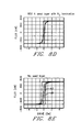
- Figs. 7A, 7B and 7C are plots of the BH loop for the easy magnetic axis 71 and the hard magnetic axis 73 for N 2 -doped, air-doped and undoped sendust films, respectively.
- the BH loops for the easy and hard magnetic axes for both the N 2 - and air-doped sendust multilayered films show a significant improvement when compared to the BH loops for the non-doped sendust films.
- the data shown in Table I and Figs. 7A, 7B and 7C are for sendust films wherein the alloy composition, by weight, was nominally Si(9.6%)Al(5.5%)Fe(84.9%).
- the doping gas used was N 2 at a partial pressure of 7.0x10 -4 Torr for the N 2 -doped sendust layers and air at a partial pressure of 7.0x10 -4 Torr for the air-doped sendust layers.
- the doping frequency and duration was 12 seconds every 120 seconds during the sputter deposition operation.
- the data shown in Table I and Figs. 7A, 7B and 7C and the improvement in soft magnetic properties obtained by the gas-doped lamination technique is expected for alloy compositions relatively close to the sendust composition used to obtain this data.
- the gas can be air, N 2 , O 2 or H 2 O, or any combination of N 2 , O 2 or H 2 O.
- the data obtained for the air- and N 2 -doped films suggest that N 2 , N 2 /O 2 and N 2 /O 2 /H 2 O gas mixtures produce generally similar effects, at least when N 2 is the primary constituent.
- the presence of O 2 or H 2 O is advantageous for optimizing a particular magnetic property.
- gas-doped sendust layer thicknesses and doping levels preferably are in the range of 10-1,000 Angstroms and 1-10 atomic percent, respectively, while the non-doped layer has a thickness in the range of 20-10,000 Angstroms.
- While the gas-doped multilayered sendust films described above with reference to Figs. 4 arid 7A - 7C provide greatly improved magnetic properties for sendust alloy having a composition by weight in the range of Si(7.5 to 13.0%)Al(2.0 to 7.0%) and the remainder Fe, the important magnetic properties of thin films of sendust, such as magnetostriction, anisotropy field and coercivity, for example, depend strongly on the composition of the sendust alloy. For example, significant improvement in magnetic properties is exhibited by sendust films having a composition at or near Si(9.6%)Al(5.4%)Fe(85.0%). Sendust films having good anisotropy field and soft magnetic properties can be obtained over only a relatively narrow range of alloy compositions.
- a seed layer of sendust having a composition which differs from the composition of a bulk layer of sendust overlaying the seed layer provides improved anisotropic field and soft magnetic properties for the bulk sendust layer for sendust compositions covering a relatively broad range outside the range of compositions for which good properties have been achieved in the prior art.
- Fig. 5 is a sectional view of a second preferred embodiment of a multilayered sendust film according to the principles of the present invention.
- the multilayered sendust film structure 50 comprises a seed layer 53 of a sendust alloy having a first composition deposited over a base layer 52 on a substrate 51.
- a bulk sendust layer 55 having a second composition is deposited over the seed layer 53.
- the sendust alloys utilized have a composition by weight in the range of Si(7.5 to 13.0%)Al(2.0 to 7.0%) and the remainder Fe.
- multilayered sendust films including a seed layer 53 and a bulk layer 55 were deposited on a substrate 51/52 by an RF diode sputtering process in a Perkin-Elmer 4400 sputter deposition system.
- the substrate 51 comprised a ceramic material, 70 percent Al 2 O 3 - 30 percent Tic, coated with a 3.5 micrometer base layer 52 of sputtered alumina having a lapped surface.
- the seed layers 53 for the films 50 were deposited by co-sputtering from two sendust targets having a nominal composition, by weight, of Si(9.6%)Al(6.0%)Fe(84.4%) (composition A).
- the bulk layer 55 was deposited from a single sendust target without breaking vacuum.
- the bulk layer 55 was deposited from a sendust target having a nominal composition, by weight, of Si(12.0%)Al(4.5%)Fe(83.5%) (composition B).
- the bulk layer 55 was deposited from a sendust target having a nominal composition, by weight, of Si(11.5%)Al(5.0%)Fe(83.5%) (composition C).
- the seed layer 53 can be uniformly doped by a gas, such as N 2 or O 2 , by introducing a partial pressure of the doping gas into the deposition environment during deposition of the seed layer 53, as described above.
- the seed layer 53 thickness was in a range of 100 - 800 Angstroms.
- the bulk layer 55 thickness was in a range of 0.3 - 10.0 micrometers.
- the multilayered film 50 comprises a seed layer 53, 320 Angstroms thick layer of sendust, composition A, uniformly doped with N 2 at a partial pressure of 7X10 -4 Torr during deposition, and a bulk layer 55 of negative lambda sendust, composition B, 1.85 micrometers thick deposited on the seed layer. After deposition, the sendust films 50 were annealed at 470 degrees C for 4.5 hours in a magnetic field filed under a N 2 atmosphere.
- Fig. 6 is a sectional view of another preferred embodiment of the multilayered sendust film described with reference to Fig. 5.
- the multilayered sendust film 60 comprises a seed layer 63 of sendust having a first composition and a bulk layer 65 of sendust having a second composition deposited over the seed layer 63 wherein the seed layer 63 comprises alternating layers of gas-doped sendust 67 and sendust 69 as described above with reference to Fig. 4.
- sendust films comprising a seed layer 63 and a bulk layer 65 were sputter deposited on a substrate 61 over a base layer 62 of alumina as described above for the films shown in Fig. 5.
- the above-described N 2 doping process was used to provide the seed layer 63 having alternating layers of N 2 -doped sendust and non-doped sendust of sendust composition A.
- the N 2 -doped layers 67 were 16 Angstroms thick while the non-doped sendust layers 69 were 145 Angstroms thick.
- the doped and non-doped layers can have thicknesses in the range of 10 to 2,000 Angstroms.
- Table II provides typically obtained values for key magnetic properties of selected sendust films 50 and 60 having bulk layers 55, 65 of sendust composition B or C and seed layers 53, 63 of sendust composition A.
- H ce and H ch are the easy axis and the hard axis coercivity
- MU i and MU r are the initial and remnant permeability
- B r /B s is the ratio of the remnant induction to the saturation induction on the hard magnetic axis.
- N 2 specifies whether or not the seed layer comprised alternating N 2 -doped and non-doped layers (as described above with reference to Fig. 6), a single, uniformly doped layer or a single non-doped layer.
- those films having a single layer uniformly-doped seed layer exhibit improved anisotropic properties when compared to the films having non-doped seed layers.
- the resulting anisotropic properties are a function of the seed layer thickness with minimum values for H ch and B r /B s occurring at a thickness of 320 Angstroms.
- Figs. 8A, 8B and 8C are plots of the easy magnetic axis 81 and the hard magnetic axis 83 for the sendust films having a bulk layer 55, 65 of sendust composition B for a film with a seed layer 53 of 800 Angstroms thickness, for a film with a N 2 -doped seed layer 63 of 800 Angstroms thickness and for a film with no seed layer, respectively.
- the sendust films having a seed layer 63 comprising alternating layers of N 2 -doped sendust 67 and non-doped sendust 69 provide the greatest overall improvement, for example, Fig. 8B shows that the BH loop for the hard magnetic axis is essentially closed.
- Figs. 8D and 8E are plots of the easy magnetic axis 81 and the hard magnetic axis 83 for the films having a bulk layer of sendust composition C for a N 2 -doped seed layer 63 of 800 Angstroms thickness and for a film with no seed layer, respectively.
- the effect of the N 2 - doped seed layer 63 in creating highly anisotropic sendust films is clearly illustrated when the BH loop plots of the hard magnetic axis 83 of Figs. 8D and 8E are compared.
- the final sendust film, having bulk sendust composition A and no seed layer, shown in Table II exhibits acceptable values for the anisotropic and soft magnetic properties required for MR head shield applications.
- the sendust film with no seed layer having the B composition exhibits relatively poor anisotropic properties
- the sendust film with no seed layer having the C composition exhibits properties which are marginally acceptable.
- a seed layer for films of sendust composition B and C provides films having excellent anisotropic and soft magnetic properties for applications as shields in MR heads and pole tip material in inductive heads.
- Films fabricated from sputtering targets having compositions in the range near the composition of compositions B and C are particularly desirable because these compositions produce sendust films having negative and near-zero values of magnetostriction, respectively.
- sendust films of composition A provide satisfactory anisotropic and soft magnetic properties with no seed layer, such films exhibit positive values of magnetostriction.
- negative or near-zero magnetostriction films are required to maintain the most desirable magnetic domain configuration at the head ABS after it is lapped.
- the MR read head assembly 90 comprises a first shield member 91 which is separated from a substrate 92 by a nonconductive layer 94 of alumina, for example.
- Substrate 92 typically comprises the body of a slider which supports the MR head on the trailing edge thereof as shown in Fig. 3.
- the first shield 91 is also referred to as the leading shield with respect to the relative motion between the slider and the magnetic storage medium surface as indicated by arrow 96.
- a first nonmagnetic gap layer 98 is then deposited over the first shield 91 to serve as a base layer for deposition of the MR sensor element 93.
- MR sensor element 93 is shown as having a single layer, it will be apparent to those skilled in the art that additional layers for properly biasing the sensor, for example, may also be included.
- the MR sensor element is contacted by electrically conductive leads 95, which are isolated from the second shield member 97 by a second nonmagnetic gap layer 99.
- a protective layer 96 is then deposited to a desired thickness at the trailing end of the head assembly.
- the first shield 91 comprises a multilayered thin film structure including a seed layer 101 of sendust of a first composition and a bulk layer 103 of sendust of a second composition as described above with reference to Fig. 5.
- the seed layer 101 comprises multilayered structure of alternating layers of gas-doped sendust of said first composition and of non-doped sendust of said first composition as described above with reference to Figs. 4 and 6. Because of temperature and other process limitations imposed on the MR head assembly 90 by the preferred materials for the MR sensor element 93, generally only the first shield 91 will be of sendust alloy while the second shield will be of a material having the required anisotropic field and soft magnetic properties such as permalloy, for example.
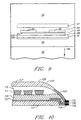
- the inductive head 110 comprises a flat conductor coil 111 plated in an elliptical pattern between two layers 113, 115 of insulating material such as alumina, for example.
- the coil 111 is inductively coupled to a magnetic yoke structure 117 having two composite layers each including a pole tip region and a back region and having a back gap region magnetically coupling the two layers which extends through the coil 111 (not shown).
- the lower layer has a pole tip portion 119 and a back region 121 and the upper layer has a pole tip portion 123 and a back region 125.
- the yoke layers 119, 123 are separated by a gap material layer 127 that defines the transducing gap 128.
- the balance of the yoke layers are separated by the insulating layers 113, 115 in addition to the gap material layer 127 with the exception of the back gap region where the upper and lower yoke layers are in intimate contact.
- the dimensions of the pole tips in the gap 128 region at the ABS are relatively small providing a relatively small volume of magnetic material to carry the magnetic flux when compared to the remainder of the pole tips 119, 123 and the lower and upper back region layers 121, 125 remote from the gap 128 region.
- the majority of the magnetic yoke structure 117 can be of any suitable magnetic material having appropriate magnetic properties, such as NiFe, NiFeCo or plain iron, for example, that portion of the pole tip regions 119, 123 at the gap 128 requires a material having a high saturation magnetization.
- the pole tip regions 119 and 121 of the yoke structure comprise a multilayered structure consisting of alternating layers of gas-doped sendust and non-doped sendust as described above with respect to Fig. 4.
- the pole tip regions 119 and 123 of the yoke structure comprise a multilayered structure consisting of a seed layer of sendust having a first composition and a bulk layer of sendust having a second composition as described above with reference to Figs. 5 and 6.
- the seed layer can comprise a single layer of sendust or can be a multilayered structure consisting of alternating layers of gas-doped sendust and non-doped sendust.
- the back region layers 121, 125 and the portions of the pole tip layers 119, 123 remote from the ABS can be fabricated of a suitable magnetic material such as permalloy, for example, while only the pole tip portions 129, 131 in the gap 128 region exposed at the ABS are formed of the multilayered sendust structures described above with reference to Figs. 4, 5 and 6.
- pole tips 129 and 131 can comprise a structure having a seed layer of a first sendust composition and a bulk layer of a second sendust composition wherein the seed layer comprises either a single layer of sendust or a multilayered structure of alternating gas-doped sendust layers and sendust layers.
- a merged transducer as shown essentially comprises an MR read head and an inductive write head formed one on top of the other in such a manner that lower magnetic pole piece of the inductive head and the second or upper magnetic shield element of the MR head can be combined into a single shielding element.
- the merged MR-read/inductive-write transducer assembly 130 comprises a first shield member 131 which is separated from a substrate 132 by a nonconductive layer 134 of alumina, for example.
- Substrate 132 typically comprises the body of a slider which supports the transducer on the trailing edge thereof as shown in Fig. 3.
- a first nonmagnetic gap layer 139 is then deposited over the first shield 131 to serve as a base layer for deposition of the MR sensor element 133.
- MR sensor element 133 is shown as having a single layer, it will be apparent to those skilled in the art that additional layers for properly biasing the sensor, for example, may also be included.
- the MR sensor element is contacted by electrically conductive leads 135, which are isolated from the second shield member 137 by a second magnetic gap layer 141.
- the second shield member 137 comprises a single element which serves as both an upper shield for the MR sensor element 133 and as the lower pole piece for the inductive write head.
- the second shield member 137 is fabricated of a material having suitable magnetic and mechanical properties such as NiFe, for example, as is known in the art. Then a layer of a nonmagnetic gap material and an upper pole piece having pole tip 143 are deposited over the lower pole piece and machined to the desired dimensions by ion beam milling or other suitable process forming magnetic gap 145. The inductive coil and remaining portions of the upper pole piece (not shown) are fabricated as is known in the art. A protective layer 136 is then deposited to a desired thickness at the trailing end of the transducer assembly.
- first shield 131 comprises a multilayered thin film structure including a seed layer 149 of sendust of a first composition and a bulk layer 151 of sendust of a second composition as described above with reference to Fig. 5.
- the seed layer 149 comprises a multilayered structure of alternating layers of gas-doped sendust 153 of said first composition and of non-doped sendust 155 of said first composition as described above with reference to Figs. 4 and 6.
Landscapes
- Engineering & Computer Science (AREA)
- Manufacturing & Machinery (AREA)
- Chemical & Material Sciences (AREA)
- Nanotechnology (AREA)
- Power Engineering (AREA)
- Crystallography & Structural Chemistry (AREA)
- Physics & Mathematics (AREA)
- Spectroscopy & Molecular Physics (AREA)
- Electromagnetism (AREA)
- Condensed Matter Physics & Semiconductors (AREA)
- General Physics & Mathematics (AREA)
- Magnetic Heads (AREA)
- Thin Magnetic Films (AREA)
- Physical Vapour Deposition (AREA)
Claims (29)
- Une structure magnétique en couches (50), conçue pour utilisation dans une tête magnétique d'enregistrement et/ou de relecture, en au moins des première et deuxième couches, ladite première couche (53) formant une couche d'ensemencement, ladite deuxième couche (55) formant une couche massive d'un alliage de silicium-aluminium-fer (SiAlFe) ayant une première composition, ladite deuxième couche étant formée sur ladite première couche,
et caractérisée en ce que ladite première couche est constituée d'un alliage SiAlFe ayant une deuxième composition qui est différente de ladite première composition. - La structure magnétique en couches selon la revendication 1, dans laquelle ladite première couche en alliage SiAlFe est constituée d'un alliage ayant une composition, en poids, de 7,5 à 13,0 pour-cent en Si, 2,0 à 7,0 pour-cent en Al et le reste en Fe, et ladite deuxième couche d'alliage SiAlFe étant constituée d'un alliage ayant une composition de 7,5 à 13,0 pour-cent en Si, 2,0 à 7,0 pour-cent en Al, et le reste en Fe.
- La structure magnétique en couche selon la revendication 2, dans laquelle ladite première couche en alliage SiAlFe est constituée d'environ 9,6 pour-cent en Si, 6,0 pour-cent en Al, et le reste en Fe.
- La structure magnétique en couche l'une quelconque des revendications précédentes, dans laquelle ladite couche d'ensemencement comprend une couche de ladite deuxième composition d'alliage SiAlFe, dopée avec un gaz sélectionné.
- La structure magnétique en couche selon la revendication 4, dans laquelle ledit gaz sélectionné comprend un gaz choisi dans le groupe composé de l'azote (N2), l'oxygène (O2), la vapeur d'eau (H2O) et l'air et des mélanges de N2 avec O2 et avec des mélanges O2/H2O.
- La structure magnétique en couche selon la revendication 5, dans laquelle ledit gaz sélectionné comprend du N2.
- La structure magnétique en couche selon la revendication 5, dans laquelle ledit gaz sélectionné comprend l'air.
- La structure magnétique en couche selon l'une quelconque des revendications 4 à 7, dans laquelle ladite couche d'ensemencement comprend au moins une couche dopée (67) de ladite deuxième composition SiAlFe, dopée avec un gaz sélectionné, et au moins une couche non dopée (69) de ladite deuxième composition d'alliage SiAlFe, lesdites couches dopées et non dopées étant laminées alternativement.
- La structure magnétique en couche selon la revendication 8, dans laquelle lesdites couches dopées ont une épaisseur située dans la plage d'environ 10 Angströms à environ 2000 Angströms et lesdites couches non-dopées ont une épaisseur située dans la plage d'environ 10 Angströms à environ 2000 Angströms.
- La structure magnétique en couche selon la revendication 9, dans laquelle lesdites couches dopées ont une épaisseur d'environ 16 Angströms et lesdites couches non-dopées ont une épaisseur d'environ 145 Angströms.
- Ladite structure magnétique en couche selon l'une quelconque des revendications précédentes, dans lequelle ladite couche massive a une épaisseur dans la plage de 0,3 à 10,0 micromètres.
- La structure magnétique en couche selon la revendication 11, dans laquelle ladite couche d'ensemencement a une épaisseur d'environ 900 Angströms et ladite couche massive une épaisseur d'environ 1,9 micromètres.
- La structure magnétique en couche selon la revendication 11, dans laquelle ladite couche d'ensemencement a une épaisseur d'environ 320 Angströms et ladite couche massive a une épaisseur d'environ 1,85 micromètres.
- La structure magnétique en couche selon l'une quelconque des revendications 1 à 11, dans laquelle ladite couche d'ensemencement a une épaisseur dans la plage de 100 Angströms à 800 Angströms.
- La structure magnétique en couche selon l'une quelconque des revendications précédentes, dans laquelle dans laquelle ladite couche massive comprend un alliage sendust ayant une magnétostriction proche de zéro ou négative.
- La structure magnétique en couche selon la revendication 15, dans laquelle ladite couche massive comprend un alliage sendust ayant une magnétostriction négative.
- La structure magnétique en couche selon les revendications 15 ou 16, dans laquelle ladite couche massive comprend un alliage SiAlFe de composition en poids sensiblement de 12,0 pour-cent en Si, 4,5 pour-cent en Al, et le reste en Fe.
- La structure magnétique en couche selon les revendications 15 ou 16, dans laquelle ladite couche massive est constituée d'un alliage SiAlFe ayant une composition, en poids sensiblement de 11,5 pour-cent en Si, 5,0 pour-cent en Al, et le reste en Fe.
- Un transducteur magnétorésistif blindé comprenant :un premier élément de blindage magnétique (91), constitué d'une structure magnétique en couche selon l'une quelconque des revendications précédentes;une première couche (98), constituée d'un matériau isolant électriquement, formée sur ledit premier élément de blindage;un élément capteur magnétorésistif (93) d'un matériau magnétique formé sur ladite première couche isolante;une deuxième couche (99) d'un matériau isolant à l'électricité, formée sur l'élément capteur magnétorésistif; etun deuxième élément de blindage magnétique (97), constitué d'un matériau magnétiquement doux, formé sur ladite deuxième couche isolante.
- Un transducteur magnétique inductif comprenant :une première pièce polaire magnétique (129);une couche magnétiquement isolante, formée sur ladite première pièce polaire magnétique et constituée d'une première couche à entrefer magnétique (127).une deuxième pièce polaire magnétique (131), formée pour fournir un circuit magnétique avec ladite première pièce polaire magnétique, lesdites première et deuxième pièces polaires magnétiques ayant chacune une zone de bout de pôle, formée en relation d'espacement et d'opposition vis-à-vis de ladite couche d'entrefer magnétique disposée entre elles et formant un entrefer magnétique; etdes bobines conductrices (11), formées entre lesdites première et deuxième pièces polaires magnétiques, couplées de façon inductive vis-à-vis dudit circuit magnétique;chacun desdits premier et deuxième bouts de pôle de pièce polaire étant constitué d'une structure magnétique selon l'une quelconque des revendications 1 à 18.
- Un transducteur mixte à lecture magnétorésistive/écriture inductive, comprenant :un premier élément de blindage magnétique (131) constitué d'une structure magnétique en couche selon l'une quelconque des revendications 1 à 18;une première couche (139) constituée d'un matériau isolant de l'électricité, formée sur le premier élément de blindage;un élément capteur magnétorésistif (133), constitué d'un matériau magnétique, formé sur ladite première couche isolante:une deuxième couche (141) constituée d'un matériau isolant à l'électricité, formée sur ledit élément capteur magnétorésistif;un deuxième élément de blindage magnétique (137), constitué d'un matériau magnétiquement doux, formé sur ladite deuxième couche isolante, ledit deuxième élément de blindage magnétique formant également une première pièce polaire magnétique;une couche d'isolation magnétique (145), formée sur une face supérieure dudit deuxième élément de blindage magnétique et constituant une couche d'entrefer magnétique;une deuxième pièce polaire magnétique (143), formée pour fournir un circuit magnétique avec ledit deuxième élément de blindage magnétique, ladite deuxième pièce polaire magnétique ayant un bout de pôle formé en relation d'espacement et d'opposition vis-à-vis dudit premier bout de pôle magnétique, ladite couche d'entrefer magnétique disposée entre elles formant un entrefer magnétique; etdes bobines conductrices, formées sur ladite couche d'entrefer magnétique, entre ledit deuxième élément de blindage magnétique et ladite deuxième pièce polaire magnétique, lesdites bobines conductrices étant couplées par voie inductive vis-à-vis dudit circuit magnétique.
- Un système de stockage magnétique comprenant un milieu de stockage magnétique (12) ayant une pluralité de pistes de données, destinées a enregistrer des données, et un transducteur magnétique (21), tel que selon les revendications 19, 20 ou 21, maintenu en position d'espacement rapproché par rapport audit milieu de stockage magnétique, pour effectuer un transfert de données avec lui.
- Un procédé de fabrication d'une structure magnétique en couche, pour utilisation dans une tête magnétique d'enregistrement et/ou de relecture, comprenant au moins des première et deuxième couches, le procédé comprenant les étapes consistant à :former ladite première couche (53) à titre de couche d'ensemencement;et former ladite deuxième couche (55) à titre de couche massive sur ladite première couche, ladite deuxième couche étant constituée d'un alliage silicium-aluminium-fer (SiAlFe) ayant une première composition;et caractérisé en ce que ladite première couche est formée d'un alliage SiAlFe ayant une deuxième composition qui est différente de ladite première composition.
- Le procédé selon la revendication 23, dans lequel ladite première couche d'alliage SiAlFe est constituée d'un alliage d'une composition de 7,5 à 13,0 pour-cent en Si, 2,0 à 7,0 pour-cent en Al et le reste en Fe, et ladite deuxième couche d'alliage SiAlFe étant constituée d'un alliage ayant une composition de 7,5 à 13,0 pour-cent en Si, 2,0 à 7,0 pour-cent en Al, et le reste en Fe.
- Le procédé selon les revendications 23 ou 24, dans lequel l'étape de formation de ladite première couche comprend la formation d'une couche unique de ladite deuxième composition d'alliage SiAlFe, dopée de façon uniforme avec un gaz sélectionné.
- Le procédé selon la revendication 23 ou 24, dans lequel l'étape de formation de ladite première couche comprend les étapes consistant à :former au moins une couche dopée (67) de ladite deuxième composition d'alliage SiAlFe dopée avec un gaz sélectionné; etformer au moins une couche non-dopée (69) constituée de ladite deuxième composition d'alliage SiAlFe, lesdites couches dopées et non-dopées étant alternativement laminées.
- Le procédé selon les revendications 25 ou 26, dans lequel ledit gaz sélectionné comprend un gaz choisi dans le groupe composé de l'azote (N2), l'oxygène (O2), la vapeur d'eau (H2O) et l'air et des mélanges de N2 avec O2 et avec des mélanges O2/H2O.
- Le procédé selon la revendication 27, dans lequel ledit gaz sélectionné comprend du N2.
- Le procédé selon la revendication 27, dans lequel ledit gaz sélectionné comprend l'air.
Applications Claiming Priority (2)
| Application Number | Priority Date | Filing Date | Title |
|---|---|---|---|
| US402393A | 1993-01-15 | 1993-01-15 | |
| US4023 | 2001-11-16 |
Publications (3)
| Publication Number | Publication Date |
|---|---|
| EP0606750A2 EP0606750A2 (fr) | 1994-07-20 |
| EP0606750A3 EP0606750A3 (fr) | 1994-10-26 |
| EP0606750B1 true EP0606750B1 (fr) | 1998-11-04 |
Family
ID=21708755
Family Applications (1)
| Application Number | Title | Priority Date | Filing Date |
|---|---|---|---|
| EP93310325A Expired - Lifetime EP0606750B1 (fr) | 1993-01-15 | 1993-12-20 | Structure magnétique en couches pour utilisation dans une tête magnétique |
Country Status (8)
| Country | Link |
|---|---|
| US (2) | US5543989A (fr) |
| EP (1) | EP0606750B1 (fr) |
| JP (1) | JP2603433B2 (fr) |
| KR (1) | KR0160751B1 (fr) |
| CN (1) | CN1077705C (fr) |
| DE (1) | DE69321930T2 (fr) |
| MY (2) | MY119423A (fr) |
| SG (1) | SG46191A1 (fr) |
Families Citing this family (28)
| Publication number | Priority date | Publication date | Assignee | Title |
|---|---|---|---|---|
| JP3382084B2 (ja) * | 1995-04-10 | 2003-03-04 | シャープ株式会社 | 磁気ヘッド用磁性薄膜およびその製造方法ならびに該磁性薄膜を用いた磁気ヘッド |
| US5901001A (en) * | 1996-02-20 | 1999-05-04 | Seagate Technology, Inc. | Detection of asperities in recording surface of storage medium |
| KR100265986B1 (ko) * | 1997-01-31 | 2000-09-15 | 가타오카 마사타카 | 복합형 박막자기헤드 및 그 제조방법 |
| FR2762922B1 (fr) * | 1997-02-19 | 2000-08-18 | Alps Electric Co Ltd | Tete magnetique a combinaison de couches minces magnetoresistive/inductive et son procede de fabrication |
| KR20010005788A (ko) * | 1997-03-28 | 2001-01-15 | 미가쿠 다카하시 | 자기저항 소자의 제조방법 |
| US6071007A (en) * | 1997-05-21 | 2000-06-06 | Seagate Technology, Inc. | Thermal asperity detection head |
| US6337783B1 (en) | 1998-08-12 | 2002-01-08 | International Business Machines Corporation | Write head with multi-stitched second pole piece |
| US6632520B1 (en) * | 1998-09-03 | 2003-10-14 | Matsushita Electric Industrial Co., Ltd. | Magnetic film |
| US6169646B1 (en) | 1998-11-18 | 2001-01-02 | Seagate Technology, Inc. | Magnetoresistive shield incorporating seedlayer for anisotropy enhancement |
| US6222707B1 (en) | 1998-12-28 | 2001-04-24 | Read-Rite Corporation | Bottom or dual spin valve having a seed layer that results in an improved antiferromagnetic layer |
| US6342311B1 (en) | 1999-10-08 | 2002-01-29 | Seagate Technology, Inc. | High magnetic moment seed layer materials for writer pole tips |
| US6411476B1 (en) * | 1999-10-28 | 2002-06-25 | International Business Machines Corporation | Trilayer seed layer structure for spin valve sensor |
| US6519119B1 (en) | 1999-11-03 | 2003-02-11 | Seagate Technology, Llc | Structure for current perrpendicular to plane giant magnetoresistive read heads |
| US6524730B1 (en) | 1999-11-19 | 2003-02-25 | Seagate Technology, Llc | NiFe-containing soft magnetic layer design for multilayer media |
| US6417990B1 (en) | 1999-12-06 | 2002-07-09 | Seagate Technology Llc | Composite core structure for high efficiency writer |
| JP3943337B2 (ja) * | 2000-11-10 | 2007-07-11 | Tdk株式会社 | 薄膜磁気ヘッドの製造方法 |
| US6700757B2 (en) | 2001-01-02 | 2004-03-02 | Hitachi Global Storage Technologies Netherlands B.V. | Enhanced free layer for a spin valve sensor |
| JP3971934B2 (ja) | 2001-03-07 | 2007-09-05 | ヤマハ株式会社 | 磁気センサとその製法 |
| US7241951B2 (en) * | 2001-06-29 | 2007-07-10 | Pirelli & C. S.P.A. | Method for shielding the magnetic field generated by an electrical power transmission line, and magnetically shielded electrical power transmission line |
| US20030072970A1 (en) * | 2001-10-05 | 2003-04-17 | Headway Technologies, Inc. | Layered structure for magnetic recording heads |
| US6950277B1 (en) * | 2002-10-25 | 2005-09-27 | Maxtor Corporation | Concave trailing edge write pole for perpendicular recording |
| US6937018B2 (en) * | 2003-10-31 | 2005-08-30 | General Electric Company | Systems and methods for fabricating pole pieces for magnetic resonance imaging systems |
| US7446980B2 (en) * | 2004-10-29 | 2008-11-04 | Hitachi Global Storage Technologies Netherlands B.V. | Method for manufacturing a stitched “floating” trailing shield for a perpendicular recording head |
| US7359151B1 (en) * | 2005-03-30 | 2008-04-15 | Storage Technology Corporation | Magnetic head having writer with embedded write gap between wear-resistant pole tip layers |
| US7551396B2 (en) * | 2005-04-27 | 2009-06-23 | Hitachi Global Storage Technologies Netherlands B.V. | Perpendicular magnetic write head having a studded trailing shield compatible with read/write offset |
| US7639450B2 (en) * | 2005-04-27 | 2009-12-29 | Hitachi Global Storage Technologies Netherlands B.V. | Flux shunt structure for reducing return pole corner fields in a perpendicular magnetic recording head |
| US7869160B1 (en) * | 2005-04-27 | 2011-01-11 | Western Digital (Fremont), Llc | Perpendicular recording head with shaped pole surfaces for higher linear data densities |
| CN102916127A (zh) * | 2012-11-14 | 2013-02-06 | 浙江师范大学 | 一种高性能磁阻抗复合材料 |
Family Cites Families (19)
| Publication number | Priority date | Publication date | Assignee | Title |
|---|---|---|---|---|
| US4639806A (en) * | 1983-09-09 | 1987-01-27 | Sharp Kabushiki Kaisha | Thin film magnetic head having a magnetized ferromagnetic film on the MR element |
| JPS60220914A (ja) * | 1984-04-18 | 1985-11-05 | Sony Corp | 磁性薄膜 |
| JPS60220913A (ja) * | 1984-04-18 | 1985-11-05 | Sony Corp | 磁性薄膜 |
| JPH0652684B2 (ja) * | 1984-07-19 | 1994-07-06 | ソニー株式会社 | 磁性合金薄膜 |
| JPH0626167B2 (ja) * | 1985-08-09 | 1994-04-06 | ソニー株式会社 | 軟磁性薄膜 |
| US4897318A (en) * | 1986-01-21 | 1990-01-30 | Matsushita Electric Industrial Co., Ltd. | Laminated magnetic materials |
| JPS63126208A (ja) * | 1986-11-15 | 1988-05-30 | Sony Corp | 組織変調軟磁性積層膜 |
| US4945397A (en) * | 1986-12-08 | 1990-07-31 | Honeywell Inc. | Resistive overlayer for magnetic films |
| US4904543A (en) * | 1987-04-23 | 1990-02-27 | Matsushita Electric Industrial Co., Ltd. | Compositionally modulated, nitrided alloy films and method for making the same |
| US5103553A (en) * | 1987-07-29 | 1992-04-14 | Digital Equipment Corporation | Method of making a magnetic recording head |
| US4780779A (en) * | 1987-11-19 | 1988-10-25 | Ampex Corporation | Laminated sendust metal-in-gap video head |
| US5231555A (en) * | 1988-02-25 | 1993-07-27 | Nippon Mining Co., Ltd. | Magnetic head comprising a laminated magnetic layer structure between non magnetic rock salt structure oxide substrates |
| US4918554A (en) * | 1988-09-27 | 1990-04-17 | International Business Machines Corporation | Process for making a shielded magnetoresistive sensor |
| US5147732A (en) * | 1988-09-28 | 1992-09-15 | Hitachi, Ltd. | Longitudinal magnetic recording media and magnetic memory units |
| JP2775770B2 (ja) * | 1988-10-05 | 1998-07-16 | ソニー株式会社 | 軟磁性薄膜の製造方法 |
| EP0400966B1 (fr) * | 1989-05-29 | 1995-02-15 | Sharp Kabushiki Kaisha | Procédé de fabrication d'une tête magnétique |
| JP2779526B2 (ja) * | 1989-09-21 | 1998-07-23 | 株式会社日立製作所 | 複合薄膜磁気ヘッド |
| JP2712631B2 (ja) * | 1989-09-25 | 1998-02-16 | 松下電器産業株式会社 | 軟磁性薄膜及び磁気ヘッド |
| JPH03203008A (ja) * | 1989-12-28 | 1991-09-04 | Nec Kansai Ltd | 磁気ヘッド用Fe―Si―Al系強磁性合金積層膜の製造方法 |
-
1993
- 1993-12-20 SG SG1996000410A patent/SG46191A1/en unknown
- 1993-12-20 EP EP93310325A patent/EP0606750B1/fr not_active Expired - Lifetime
- 1993-12-20 JP JP5319336A patent/JP2603433B2/ja not_active Expired - Fee Related
- 1993-12-20 MY MYPI97000656A patent/MY119423A/en unknown
- 1993-12-20 DE DE69321930T patent/DE69321930T2/de not_active Expired - Fee Related
- 1993-12-20 KR KR1019930028554A patent/KR0160751B1/ko not_active Expired - Fee Related
- 1993-12-20 MY MYPI93002777A patent/MY109888A/en unknown
-
1994
- 1994-01-12 CN CN94100681A patent/CN1077705C/zh not_active Expired - Fee Related
-
1995
- 1995-05-26 US US08/452,202 patent/US5543989A/en not_active Expired - Lifetime
-
1996
- 1996-01-30 US US08/594,359 patent/US5686193A/en not_active Expired - Lifetime
Also Published As
| Publication number | Publication date |
|---|---|
| JP2603433B2 (ja) | 1997-04-23 |
| CN1077705C (zh) | 2002-01-09 |
| KR0160751B1 (ko) | 1999-01-15 |
| DE69321930T2 (de) | 1999-07-01 |
| CN1094834A (zh) | 1994-11-09 |
| EP0606750A3 (fr) | 1994-10-26 |
| MY119423A (en) | 2005-05-31 |
| MY109888A (en) | 1997-09-30 |
| SG46191A1 (en) | 1998-02-20 |
| JPH06244028A (ja) | 1994-09-02 |
| US5543989A (en) | 1996-08-06 |
| US5686193A (en) | 1997-11-11 |
| EP0606750A2 (fr) | 1994-07-20 |
| DE69321930D1 (de) | 1998-12-10 |
Similar Documents
| Publication | Publication Date | Title |
|---|---|---|
| EP0606750B1 (fr) | Structure magnétique en couches pour utilisation dans une tête magnétique | |
| EP0725386B1 (fr) | Système de stockage à disque, tête magnétique à films minces y afférant et procédé de fabrication | |
| EP0851411B1 (fr) | Tête magnétique à film mince et appareil d'enregistrement/ reproduction magnétique | |
| US5264981A (en) | Multilayered ferromagnetic film and magnetic head employing the same | |
| CA1310411C (fr) | Tete d'enregistrement magnetique a trois poles | |
| CA2064641C (fr) | Tete magnetique a piece polaire perfectionnee et methode de fabrication connexe | |
| EP0361657B1 (fr) | Procédé de réalisation d'un détecteur magnétorésistif blindé | |
| US6325947B1 (en) | Method for forming low profile multi-layer coil merged thin film magnetic head | |
| US5442507A (en) | Magnetoresistive magnetic head | |
| US5909344A (en) | Magnetoresistive sensor with high resistivity flux guide | |
| US20020154451A1 (en) | Non-magnetic metallic layer in a reader gap of a disc drive | |
| JPH09326104A (ja) | 磁気ヘッド | |
| US20030086215A1 (en) | Magnetic read element shield | |
| US6562487B1 (en) | Writer pole employing a high saturation moment, low permeability layer adjacent to writer gap | |
| US6740383B2 (en) | Magnetic recording medium possessing a ratio of Hc(perpendicular) to Hc(horizontal) that is not more than 0.22 and magnetic recording disk device | |
| US5959813A (en) | Combination read/write thin film magnetic head using a shielding magnetic layer | |
| US20020060880A1 (en) | Thin film magnetic heads and a method of producing the same | |
| US6129981A (en) | Magnetic recording medium and magnetic recording disk device | |
| US5945190A (en) | Magnetic recording medium and magnetic disk device | |
| JPH064832A (ja) | 複合型薄膜磁気ヘッド | |
| US5218499A (en) | Thin-film magnetic head for perpendicular magnetic recording having a magnetic member with grooves crossing at right angles formed in a principal surface thereof | |
| US6042897A (en) | Combination read/write thin film magnetic head and its manufacturing method | |
| Bain | Recording heads: write heads for high-density magnetic tape | |
| JPH07153022A (ja) | 薄膜磁気ヘッド | |
| JPH064831A (ja) | 薄膜磁気ヘッド |
Legal Events
| Date | Code | Title | Description |
|---|---|---|---|
| PUAI | Public reference made under article 153(3) epc to a published international application that has entered the european phase |
Free format text: ORIGINAL CODE: 0009012 |
|
| AK | Designated contracting states |
Kind code of ref document: A2 Designated state(s): DE FR GB |
|
| PUAL | Search report despatched |
Free format text: ORIGINAL CODE: 0009013 |
|
| AK | Designated contracting states |
Kind code of ref document: A3 Designated state(s): DE FR GB |
|
| 17P | Request for examination filed |
Effective date: 19941125 |
|
| 17Q | First examination report despatched |
Effective date: 19970620 |
|
| GRAG | Despatch of communication of intention to grant |
Free format text: ORIGINAL CODE: EPIDOS AGRA |
|
| GRAG | Despatch of communication of intention to grant |
Free format text: ORIGINAL CODE: EPIDOS AGRA |
|
| GRAH | Despatch of communication of intention to grant a patent |
Free format text: ORIGINAL CODE: EPIDOS IGRA |
|
| GRAH | Despatch of communication of intention to grant a patent |
Free format text: ORIGINAL CODE: EPIDOS IGRA |
|
| GRAA | (expected) grant |
Free format text: ORIGINAL CODE: 0009210 |
|
| AK | Designated contracting states |
Kind code of ref document: B1 Designated state(s): DE FR GB |
|
| REF | Corresponds to: |
Ref document number: 69321930 Country of ref document: DE Date of ref document: 19981210 |
|
| ET | Fr: translation filed | ||
| PLBE | No opposition filed within time limit |
Free format text: ORIGINAL CODE: 0009261 |
|
| STAA | Information on the status of an ep patent application or granted ep patent |
Free format text: STATUS: NO OPPOSITION FILED WITHIN TIME LIMIT |
|
| 26N | No opposition filed | ||
| PGFP | Annual fee paid to national office [announced via postgrant information from national office to epo] |
Ref country code: GB Payment date: 19991122 Year of fee payment: 7 |
|
| PG25 | Lapsed in a contracting state [announced via postgrant information from national office to epo] |
Ref country code: GB Free format text: LAPSE BECAUSE OF NON-PAYMENT OF DUE FEES Effective date: 20001220 |
|
| GBPC | Gb: european patent ceased through non-payment of renewal fee |
Effective date: 20001220 |
|
| REG | Reference to a national code |
Ref country code: FR Ref legal event code: TP |
|
| PGFP | Annual fee paid to national office [announced via postgrant information from national office to epo] |
Ref country code: FR Payment date: 20071205 Year of fee payment: 15 |
|
| PGFP | Annual fee paid to national office [announced via postgrant information from national office to epo] |
Ref country code: DE Payment date: 20071206 Year of fee payment: 15 |
|
| REG | Reference to a national code |
Ref country code: FR Ref legal event code: ST Effective date: 20090831 |
|
| PG25 | Lapsed in a contracting state [announced via postgrant information from national office to epo] |
Ref country code: DE Free format text: LAPSE BECAUSE OF NON-PAYMENT OF DUE FEES Effective date: 20090701 |
|
| PG25 | Lapsed in a contracting state [announced via postgrant information from national office to epo] |
Ref country code: FR Free format text: LAPSE BECAUSE OF NON-PAYMENT OF DUE FEES Effective date: 20081231 |