EP0607075A1 - Elektronische Anordnung, die einen negativen dynamischen Widerstand haben kann, und Verfahren zur Herstellung - Google Patents
Elektronische Anordnung, die einen negativen dynamischen Widerstand haben kann, und Verfahren zur Herstellung Download PDFInfo
- Publication number
- EP0607075A1 EP0607075A1 EP94400052A EP94400052A EP0607075A1 EP 0607075 A1 EP0607075 A1 EP 0607075A1 EP 94400052 A EP94400052 A EP 94400052A EP 94400052 A EP94400052 A EP 94400052A EP 0607075 A1 EP0607075 A1 EP 0607075A1
- Authority
- EP
- European Patent Office
- Prior art keywords
- zone
- active region
- insulating
- semiconductor
- substrate
- Prior art date
- Legal status (The legal status is an assumption and is not a legal conclusion. Google has not performed a legal analysis and makes no representation as to the accuracy of the status listed.)
- Granted
Links
Images




Classifications
-
- H—ELECTRICITY
- H10—SEMICONDUCTOR DEVICES; ELECTRIC SOLID-STATE DEVICES NOT OTHERWISE PROVIDED FOR
- H10D—INORGANIC ELECTRIC SEMICONDUCTOR DEVICES
- H10D48/00—Individual devices not covered by groups H10D1/00 - H10D44/00
- H10D48/01—Manufacture or treatment
- H10D48/031—Manufacture or treatment of three-or-more electrode devices
-
- H—ELECTRICITY
- H10—SEMICONDUCTOR DEVICES; ELECTRIC SOLID-STATE DEVICES NOT OTHERWISE PROVIDED FOR
- H10D—INORGANIC ELECTRIC SEMICONDUCTOR DEVICES
- H10D10/00—Bipolar junction transistors [BJT]
- H10D10/40—Vertical BJTs
-
- H—ELECTRICITY
- H10—SEMICONDUCTOR DEVICES; ELECTRIC SOLID-STATE DEVICES NOT OTHERWISE PROVIDED FOR
- H10D—INORGANIC ELECTRIC SEMICONDUCTOR DEVICES
- H10D12/00—Bipolar devices controlled by the field effect, e.g. insulated-gate bipolar transistors [IGBT]
-
- H—ELECTRICITY
- H10—SEMICONDUCTOR DEVICES; ELECTRIC SOLID-STATE DEVICES NOT OTHERWISE PROVIDED FOR
- H10D—INORGANIC ELECTRIC SEMICONDUCTOR DEVICES
- H10D84/00—Integrated devices formed in or on semiconductor substrates that comprise only semiconducting layers, e.g. on Si wafers or on GaAs-on-Si wafers
- H10D84/01—Manufacture or treatment
- H10D84/0107—Integrating at least one component covered by H10D12/00 or H10D30/00 with at least one component covered by H10D8/00, H10D10/00 or H10D18/00, e.g. integrating IGFETs with BJTs
- H10D84/0109—Integrating at least one component covered by H10D12/00 or H10D30/00 with at least one component covered by H10D8/00, H10D10/00 or H10D18/00, e.g. integrating IGFETs with BJTs the at least one component covered by H10D12/00 or H10D30/00 being a MOS device
-
- H—ELECTRICITY
- H10—SEMICONDUCTOR DEVICES; ELECTRIC SOLID-STATE DEVICES NOT OTHERWISE PROVIDED FOR
- H10D—INORGANIC ELECTRIC SEMICONDUCTOR DEVICES
- H10D84/00—Integrated devices formed in or on semiconductor substrates that comprise only semiconducting layers, e.g. on Si wafers or on GaAs-on-Si wafers
- H10D84/01—Manufacture or treatment
- H10D84/02—Manufacture or treatment characterised by using material-based technologies
- H10D84/03—Manufacture or treatment characterised by using material-based technologies using Group IV technology, e.g. silicon technology or silicon-carbide [SiC] technology
- H10D84/038—Manufacture or treatment characterised by using material-based technologies using Group IV technology, e.g. silicon technology or silicon-carbide [SiC] technology using silicon technology, e.g. SiGe
-
- Y—GENERAL TAGGING OF NEW TECHNOLOGICAL DEVELOPMENTS; GENERAL TAGGING OF CROSS-SECTIONAL TECHNOLOGIES SPANNING OVER SEVERAL SECTIONS OF THE IPC; TECHNICAL SUBJECTS COVERED BY FORMER USPC CROSS-REFERENCE ART COLLECTIONS [XRACs] AND DIGESTS
- Y10—TECHNICAL SUBJECTS COVERED BY FORMER USPC
- Y10S—TECHNICAL SUBJECTS COVERED BY FORMER USPC CROSS-REFERENCE ART COLLECTIONS [XRACs] AND DIGESTS
- Y10S257/00—Active solid-state devices, e.g. transistors, solid-state diodes
- Y10S257/90—MOSFET type gate sidewall insulating spacer
Definitions
- the invention relates to semiconductor components capable of having a negative dynamic resistance configuration.
- Such components make it possible in particular to produce static memory points of small dimensions, as well as signal generators or circuits for automatic regulation or stabilization of an operating point. All these functions find their applications in particular in integrated circuits for telecommunication systems.
- US Patent No. 4,032,961 describes an integrated structure capable of exhibiting negative dynamic resistance.
- the emitter contact is located on the substrate which makes it incompatible with the CMOS / BiCMOS manufacturing technologies (which group on the same silicon wafer, insulated gate transistors with N and P channel (CMOS transistor), associated for example with a bipolar NPN transistor) because, the substrate would then serve as a common emitter for all the transistors manufactured simultaneously and these would then no longer be isolated from each other.
- CMOS / BiCMOS manufacturing technologies which group on the same silicon wafer, insulated gate transistors with N and P channel (CMOS transistor), associated for example with a bipolar NPN transistor
- the invention aims to remedy this shortcoming.
- the invention therefore firstly proposes a semiconductor electronic component, capable of having a configuration of negative dynamic resistance; according to a general characteristic of the invention, this component comprises, within a semiconductor substrate, a first active region having a first type of conductivity, for example type N, and a second active region, having a second type of conductivity, for example type P, opposite to the first type, this second active region being located between the first active region and the upper face of the substrate; moreover, on the upper face of the substrate, there is provided a projecting region containing a third active region, having the first type of conductivity, for example type N, and surmounting a first part of the second active region; metallizations are respectively located in contact with the three active regions; the second active region comprises a semiconductor zone capable of being depleted, called "depletable", extending outside the first part of the second active region, and between the first active region and the upper face of the substrate ; polarizable depletion means are then provided, located in the immediate vicinity of this depletable zone, and capable
- the invention provides a solution to the problem posed by proposing a semiconductor electronic component, structurally analogous for the most part, to a vertical bipolar transistor, but not functioning as a bipolar transistor under the application of said voltage. polarization.
- the first active region can be called by analogy “emitter” or collector ", while the second active region can be called” base " , and that the third active region can be called “collector” or “emitter”.
- the depletable zone is formed by a second part of the second active region having a concentration of dopants substantially identical to that of the first part of the second active region (this first part being that located under the third active region located in the projecting part), as well as a thickness between a lower limit thickness and an upper limit thickness, these two limit thicknesses being related to the value of the dopant concentration.
- the length of the second part of the second active region, forming the depletable zone is at least equal to a limit length which can be at least of the order of 0.3 ⁇ m, and of preferably at least 0.5 ⁇ m.
- the projecting region of the semiconductor component prefferably has insulating lateral regions situated on its lateral edges and partially or totally surmounting the depletable zone.
- the component may include a metal zone surmounting an insulating layer situated on the upper face of the substrate above the depletable zone, the stacking of metal zone - insulating layer - depletable zone - first region active then forming an insulated gate field effect transistor whose metal area forms the gate and whose deplorable area forms the channel region.
- the depletion means may include the junction between the first active region ("collector") and the second part forming the depletable area ("intrinsic base"). They can also include the gate of the insulated gate field effect transistor.
- each insulating lateral region advantageously comprises a portion situated on the lateral edge of the third active region, extended substantially square by a portion forming said insulating layer of the insulated gate field effect transistor; the metallization located in contact with the third active region then incorporates the metal area forming the gate of the transistor.
- the negative dynamic resistance is obtained from the current-voltage relationship taken at the level of the active region which would be considered as the collector of a bipolar transistor.
- a first layer is deposited on the substrate and the projecting part. insulating, and an etching of this first insulating layer is carried out to form on either side of the projecting side insulating regions at least partially overcoming the thinned area of the first semiconductor layer; on each side of the insulating lateral regions and outside the thinned zone, an overdoping of the first layer is carried out to form an overdoped zone on which the corresponding contact location will be defined, the distance separating this overdoped zone of the part of the first semiconductor layer located under the semiconductor protruding zone, defining the length of the thinned zone.
- This length of the thinned zone can be defined by etching the insulating lateral regions to give them, at their base resting on the substrate, a thickness substantially equal to said length; in this case, the first semiconductor layer is overdoped on the semiconductor block thus formed, the insulating lateral regions serving as masks.
- first insulating layer to form first insulating side regions partially overcoming said thinned zone, these first side regions being for example composed of silicon dioxide; a thin insulating layer, for example also silicon dioxide, is then deposited on the upper surface of the semiconductor block thus formed, then an additional insulating layer is deposited in an insulating material, for example nitride silicon, different from that forming the thin insulating layer and the first insulating lateral regions; this additional insulating layer is then etched to form second insulating lateral regions covering the first; the first and second insulating lateral regions as well as the thin insulating layer situated between them then form said insulating lateral regions having a thickness substantially equal to the length of the thinned zone; then removing the part of the insulating thin layer located outside the insulating side regions.
- the insulating lateral regions can also be engraved to give them a thickness at their base, less than the desired length of the thinned area; there is then deposited on the semiconductor block thus formed a mask projecting on either side of the insulating lateral regions by a distance equal to the difference between the length desired for the thinned zone and the thickness of these insulating lateral regions, and the first semiconductor layer is overdoped on the semiconductor block provided with this protruding mask.
- the insulating lateral regions are removed and another insulating layer is deposited comprising a part located on the lateral edges of the projecting part of the block and a part extending substantially square to this lateral part, and, in step e), metallization is carried out in contact with the zone protruding semiconductor, extending into a metallic zone extending over the terminal square part of the insulating layer.
- the substrate incorporates, next to the first semiconductor zone, another semiconductor zone within which an insulated gate field effect transistor is produced simultaneously whose active drain and source regions have the second type of conductivity (for example type P) and are implanted according to two successive implantations of selected dopants (LDD implantation), advantageously, in step c) the upper face of the first semiconductor layer is masked before performing the first implantation of the drain and source zones of the insulated gate field effect transistor.
- LDD implantation two successive implantations of selected dopants
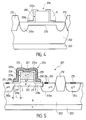
- the component 1 is produced within a semiconductor zone or box 2, having a first type of conductivity, here type N (electron conduction), incorporated within a semiconductor substrate 3 having a second type of conductivity, opposite to the first, here type P (conduction by holes).
- type N electron conduction
- P conduct by holes
- the box 2 incorporates an overdoped zone 4 N++ on which is located metallization 15.
- an overdoping of the N++ (or P++) type is equivalent to a concentration of electrons (or holes) approximately equal to 1020cm ⁇ 3 while in an N (or P doped region) ) the concentration of electrons (or holes) is of the order of 1017cm ⁇ 3 or less.
- the component 1 comprises a second region 10 having the second type of conductivity, here the P type, extending within the well N from the upper face 5 of the substrate.
- This second region 10 has a central part 10a having a P doping concentration, framed by an overdoped area P 10 10th on which a contact metallization 14 is provided.
- a projecting region 6 surmounts the upper face 5 of the substrate (or of the second region 10) above the P-doped central part of the second region.
- This projecting region 6 comprises in its central part, a region 7, composed for example of polysilicon, having the first type of conductivity, and Nd overdoped.
- a layer 8 of N+ doped silicon surmounting the central part 10a of the P doped region 10.
- the protruding region 6 also includes, on either side of the regions 7 and 8, lateral insulating regions 9, or spacers, composed for example of silicon dioxide SiO2. At the top of this protruding region 6 is provided, in contact with the overdoped silicon N++, a contact metallization 13.
- the second region 10 has a thinned zone relative to the central part 10a situated under the layer 8 of silicon N+.
- This thinned zone 10b has a length L and a thickness E. It also by nature has the same concentration of dopants as the central part 10a. It will be seen below that this thinned part or zone 10b forms a depletable zone Z capable of being depleted by depletable means which can be polarized under the action of a chosen bias voltage.
- depletion means are here formed by the junction 11 between the box N and the second region 10.
- the structure of the electronic component according to the invention is for the most part analogous to a conventional structure of a vertical bipolar transistor, such as that produced according to the BiCMOS manufacturing technology.
- the structural difference with a vertical bipolar transistor resides here in the presence of a depletable zone having a doping and selected dimensions, instead of an implanted zone doped P+ for example, defining a non-uniform doping of the known extrinsic base by a person skilled in the art under the term LDEB (Lightly doped extrinsic base).
- LDEB Lightly doped extrinsic base
- the first active region defined here by the box 2 and the contact location 4 can be, by analogy, designated by the term collector (the box N proper defining the intrinsic collector while the overdoped region 4 defines the extrinsic collector).
- the second region 10 can be considered as the second "basic" active region, in which the overdoped regions 10e define the extrinsic base.
- the third active region, formed by regions 7 and 8 can be likened to an "emitter" region in which the Nd overdoped region defines the extrinsic emitter while the N+ doped region defines the intrinsic emitter.
- emitter for simplification purposes, the terms emitter, base and collector will be used although these, as explained above, are not really suitable for the component according to the invention, the operation of which, as will be seen in more detail below, does not resemble that of a bipolar transistor.
- FIG. 2 partially illustrates another embodiment of a component according to the invention.
- the elements analogous or having functions analogous to those represented in FIG. 1 are assigned references increased by 100 compared to those they had in FIG. 1. Only the differences between these two figures will now be described. .
- the thickness of the spacers 109 is this time less than the length L of this depletable zone, whereas in FIG. 1, this thickness was substantially equal to the length L.
- the spacers 109 while in FIG. 1 the spacers completely overcame the part thinned 10b forming the depletable zone of the component, the spacers 109 only partially overcome, in FIG. 2, the depletable zone Z.
- the thickness E of the thinned zone 10b is of the order of 0.15 ⁇ m, with a concentration of dopants of the order of 1017cm ⁇ 3 and a length L of order of 0.5 ⁇ m, it has proved possible to deplete the Z region with a positive collector polarization of the order of a few volts by connecting the emitter to ground and applying a fixed voltage on the base of the order of 0.5 volts.
- the collector voltage is zero, the collector current is negative.
- the collector current decreases in absolute value until reaching the zero value then increases in absolute value, because the junction collector-base is less and less polarized in direct.
- the collector-base potential difference becomes positive, which polarizes the collector-base junction in reverse.
- the collector current then decreases despite the increase in the collector bias voltage, which therefore creates the characteristic of negative dynamic resistance.
- the collector current will start to increase again from a higher or lower collector voltage threshold, which is due either to a phenomenon of piercing the base or to an avalanche phenomenon in the collector-base junction.
- both the thickness E and the concentration of dopants play an essential role in the deplorable nature of the zone Z.
- this thickness E should be greater than or equal to a thickness -lower limit whose value is related to the concentration of dopants in the depletable zone. Indeed, if this thickness E is less than the lower limit thickness, the zone Z will not be depletable but it will on the contrary by nature deplete by itself in the absence of application of any bias voltage on the extrinsic manifold. In this case of course, the component according to the invention will not be able to function and have a configuration of negative dynamic resistance.
- the thickness E of this depletable zone must remain less than or equal to an upper limit thickness, also related to the concentration of dopants, but also to the value of the bias voltage which it is desired to apply to deplete the zoned. Indeed, if this thickness E is greater than this upper limit thickness, it will be difficult, if not impossible, to deplete the zone Z, with the application of reasonable bias voltages, or even with the application of high bias voltages.
- the lower limit thickness can be taken of the order 0.1 ⁇ m while the upper limit thickness can advantageously be adjusted on the order of 0.2 ⁇ m.
- these numerical values must be taken as an indication and can be adjusted more precisely for each compound produced as a function in particular of its manufacturing batch, from tests and / or simulation.
- the length L of the deplorable zone does not influence the depletable nature of this zone, it exerts an influence on the fall of the collector current. Indeed, if the length L of this zone is insufficient, significant leaks of the base current may appear, despite a complete depletion of the zone Z. It is therefore particularly advantageous to adjust the length L of this zone so that it is at least equal to a lower limit length which has been taken in this case of the order of 0.3 ⁇ m.
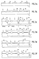
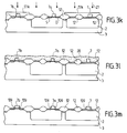
- FIGS. 3a to 3s An embodiment of a manufacturing process which in particular makes it possible to obtain the embodiments illustrated in FIGS. 1 and 2 will now be described with reference to FIGS. 3a to 3s.
- the reference 3 designates a P-doped silicon semiconductor substrate, for example, within which an N-channel insulated gate field effect transistor (NMOS) will be simultaneously produced, a field effect transistor with P-channel insulated gate (PMOS), these two transistors forming a CMOS compound, as well as the electronic component according to the invention.
- NMOS N-channel insulated gate field effect transistor
- PMOS P-channel insulated gate
- the first step then consists in defining the location of the active zones of the various components by depositing layers of nitride 16 on the upper face of the substrate 3.
- an isoboric implantation 18 is carried out after having disposed of the masks 17b on the zones in which the PMOS transistor and the component to be negative dynamic resistance.
- This isoboric implantation makes it possible in particular to prevent the phenomenon of inversion under the insulating regions (LOCOS) which will be carried out in the next step within the substrate P.
- the NMOS transistor will be produced on the left side of the substrate. Annealing after implantation is finally carried out.
- step of FIG. 3d after having placed a mask 17d above the wells 2 and 19, two implantations 21 of boron are carried out in order in particular to adjust the threshold of the NMOS transistor and to protect it against the phenomenon known as "piercing".
- step 3e the threshold of the PMOS transistor is adjusted by analogy by carrying out an implantation 22 of boron after having placed masks above the well 2 and the area of the NMOS transistor.
- a thin layer of oxide was deposited on the upper face of the substrate, including in the region of the component with negative resistance, and which will constitute in particular the gate oxides of the field effect transistors.
- This thin insulating layer is then removed above the box 2 and an implantation 23 of boron is carried out, for example on the semiconductor block provided with a mask 17f covering the areas of the field effect transistors.
- the base region 10 of the negative dynamic resistance component is thus formed.
- a layer 25 of polysilicon is then deposited (FIG. 3g) on the upper face of the substrate before undergoing an implantation 24 of arsenic for example to give it doping of the N++ type.
- an etching of this layer of doped polysilicon is carried out (FIG. 3h) in order to respectively define the gate regions 7a and 7b of the PMOS and NMOS and "emitter" 7 transistors of the negative dynamic resistance component.
- the production of the gate regions only involves etching of the doped polysilicon layer because the substrate remains isolated by a thin oxide layer.
- the etching is extended by a slight over-etching SG of the substrate, as illustrated in FIG. 3i, so as to produce, on either side of the projecting region (emitter) thus formed on the semiconductor block, a thinned zone of thickness E, part of which will form the depletable zone Z of the component with negative dynamic resistance.
- the step illustrated in FIG. 3j consists in producing the lightly doped Drain source and drain zones of the NMOS transistor by carrying out an implantation 26 of arsenic for example after having covered the semiconductor block with masks 17d placed at selected locations. Such an installation also has the effect of making contact with the well 19 of the PMOS transistor and contact with the well 2 of the component with negative dynamic resistance.
- FIGS. 3n and 3o The embodiment of the enlarged spacers 9 is illustrated in FIGS. 3n and 3o.
- a thin layer 40 of silicon dioxide is deposited on the upper surface of the semiconductor block obtained at the stage illustrated in FIG. 3m.
- a mask 17o is then deposited on the part of the semiconductor block intended to form the component with negative dynamic resistance and a chemical etching of the spacers 42 of the NMOS and PMOS transistors is carried out.
- the mask 17o is then removed and the thin layer 40 is removed.
- the configuration illustrated in FIG. 3p is then obtained, in which the assembly "spacer 109 of SiO2 - thin layer 40 of SiO2 - spacer 42 of Si3N4" forms the widened spacers 9.
- Such a method therefore makes it possible to obtain, in a simple and effective manner, spacers of different thicknesses on the same silicon wafer.
- the embodiment of the highly doped drain and source zones (PMOS) 32 illustrated in particular by the implantation 31 of boron, is illustrated after a mask 17r has been placed above the zone of the NMOS transistor, the contact location of the PMOS transistor box and the contact location 4 of the negative dynamic resistance component.
- This implantation 31 has also had the effect, since the spacers 9 of the negative dynamic resistance component form a mask, of producing the “extrinsic base” regions 10e, P, overdoped, of the component with negative dynamic resistance.
- it is the thickness at the base of the spacers which determines the length L of the depletable zone of the component with negative dynamic resistance.
- the component with negative dynamic resistance has spacers 109 having a thickness at their base smaller than the length L desired for the depletable zone, it is then advisable, as illustrated in FIG. 3s, to place above the protruding region of the component with negative dynamic resistance, a mask 17s projecting on either side of the spacers 109 by a predetermined distance equal to the difference between the desired length L for the depletable area and the thickness of the spacers counted at their base .
- the final stages of the manufacturing process consist in particular in etching the contact holes then in carrying out a rapid final annealing before proceeding with the deposition of a layer of metal or metal silicide then in etching and annealing of the interconnections thus formed .
- region N, doped N+ in the protruding "emitter" region of the component according to the invention is obtained by diffusion of dopants from the overdoped region N++, during annealing .
- the electronic component with negative dynamic resistance according to the invention is thus obtained on the same silicon wafer, in a variant similar to that illustrated in FIG. 1 (at the position near the overdoped zone 4 and LOCOS 12 which results from the choice particular illustrated in FIGS. 3a to 3s) or in a variant analogous (with the same difference) to that illustrated in FIG. 2 depending on the size of the spacers adopted, as well as PMOS and NMOS field effect transistors.
- Such a component with negative dynamic resistance is therefore compatible with a BiCMOS manufacturing technology, the substrate not serving as a common emitter.
- a person skilled in the art will have noticed that by means of the absence of the overprint SG in the step illustrated in FIG.
- the spacers 9 or 109 and the implantation of the overdoped regions 10e it is possible, after the step of making the spacers 9 or 109 and the implantation of the overdoped regions 10e, to remove these spacers to deposit a thin insulating layer 209 (FIG. 4 ) of a thickness of 150 ⁇ comprising a vertical lateral part 209a situated on the lateral edges of the projecting region 206, this part 209a being extended substantially square by a horizontal part 209b extending on the upper face of the substrate au- above the thinned part which will form the depletable zone Z of the component with negative dynamic resistance.
- the metallization disposed in contact with the active semiconductor region located in the protruding region 206 will incorporate a metallic zone disposed above the part 209b of the insulating layer.
- the metal zone 213b - insulating layer 209b - semiconductor zone 210b - box 202 stack forms a field effect transistor with an insulated gate, the thinned semiconductor part 210b of which forms the channel region.
- the regions 207 and 208 this time form a "collector” region while the regions 204 and 202 respectively form the "extrinsic emitter” and “intrinsic emitter” regions and that the region 210 always forms a "base" region.
- metallization 215 is for example connected to ground while metallization 214 is connected to a positive voltage in the present case, from 0.5 volt) for direct polarization of the junction of the first active region - second active region (emitter-base) while applying to the metallization of the third active region (collector) a bias voltage (increasing in the present case from the value 0 volts to the value of a few volts) capable of depleting the channel of the field effect transistor formed, the configuration of negative dynamic resistance always being taken at the level of the current-collector voltage couple.
- FIG. 5 The embodiments which have been described (FIGS. 1 and 2, FIG. 5) use dictational depletion means (field effect of a junction, field effect of an insulated gate field effect transistor).
- depletion means using both the field effect of a junction and the field effect of an isolated grid.
- this third active region would form an "emitter” region while the second active region would always form the "base” region and the first active region would form the "collector” region.
- the two effects of field caused on the one hand by the field effect transistor and on the other hand by the collector-base junction together would help to deplete the depletable area. n would thus be possible either to obtain a depletion of the zone more quickly with the same collector voltage of a few volts or even to obtain such a depletion while being less demanding on the conditions of dimensioning of the depletable zone (thickness, length) and / or on the dopant concentration.
- the component according to the invention could be made from another semiconductor material.
- the metallizations were carried out, in all the embodiments described, on N++ or P++ overdoped regions. Those skilled in the art know that this is preferable in the case where the semiconductor material used is silicon. However, it is possible to overcome such overdoping of these regions if a semiconductor material is used which makes it possible to directly obtain satisfactory contact with the metallizations.
- Such materials exist among the III-V materials, that is to say materials comprising in equal parts an element of the third column and an element of the fifth column of the periodic table of Mendeléeff.
- the reduction of the over-etching that is to say the increase in the thickness E of the depletable zone Z, makes it possible to limit the current leaks at the angle formed at the limit of the depletable zone Z and of the first part 110a of the second active region 110.
- this overdoped PSD substrate zone situated under the thinned zone Z is obtained by a deep implantation of dopant having the same type of conductivity as the substrate, in a part of the substrate situated under the thinned zone.
- the substrate is of type N
- the implantation of arsenic will be carried out after formation of the first insulating lateral regions 109 (FIG. 3m) and before the formation of enlarged insulating lateral regions 9 (FIGS. 3n to 3p ).
- spacers 109 are provided having a width smaller than the width L of the deplorable zone, the implantation of arsenic will advantageously be carried out before the placement of the mask 17s illustrated in FIG. 3s.
- the overdoped zone of the substrate situated under the depletable zone then extends at a distance from the limit between the depletable zone and the first part 110a of the second active region 110 which has the effect of concentrating the depletion of the deplorable zone at a distance from the corner of the spacer, so as to further limit the potential leaks.
- the deep implantation of arsenic should be replaced by a deep implantation of boron, for example.
Landscapes
- Metal-Oxide And Bipolar Metal-Oxide Semiconductor Integrated Circuits (AREA)
- Semiconductor Integrated Circuits (AREA)
Applications Claiming Priority (2)
| Application Number | Priority Date | Filing Date | Title |
|---|---|---|---|
| FR9300197 | 1993-01-12 | ||
| FR9300197A FR2700418B1 (fr) | 1993-01-12 | 1993-01-12 | Composant électronique capable de résistance dynamique négative et procédé de fabrication correspondant. |
Publications (2)
| Publication Number | Publication Date |
|---|---|
| EP0607075A1 true EP0607075A1 (de) | 1994-07-20 |
| EP0607075B1 EP0607075B1 (de) | 2003-04-16 |
Family
ID=9442957
Family Applications (1)
| Application Number | Title | Priority Date | Filing Date |
|---|---|---|---|
| EP94400052A Expired - Lifetime EP0607075B1 (de) | 1993-01-12 | 1994-01-10 | Elektronisches Halbleiterbauelement mit negativem dynamischem Widerstand und entsprechende Verwendungs- und Herstellungsverfahren |
Country Status (5)
| Country | Link |
|---|---|
| US (1) | US5465001A (de) |
| EP (1) | EP0607075B1 (de) |
| JP (1) | JP3746306B2 (de) |
| DE (1) | DE69432494D1 (de) |
| FR (1) | FR2700418B1 (de) |
Families Citing this family (3)
| Publication number | Priority date | Publication date | Assignee | Title |
|---|---|---|---|---|
| JP3333813B2 (ja) * | 1996-11-20 | 2002-10-15 | トヨタ自動車株式会社 | 乗員保護装置の起動制御装置 |
| DE60028847T2 (de) * | 1999-02-08 | 2006-12-07 | Texas Instruments Inc., Dallas | Verfahren mit reduzierter Maskenzahl für die Herstellung von Mischsspannung-CMOS mit Hochleistung-Transistoren und -I/O Transistoren von hoher Zuverlässigkeit |
| US9306042B2 (en) * | 2014-02-18 | 2016-04-05 | International Business Machines Corporation | Bipolar transistor with carbon alloyed contacts |
Citations (8)
| Publication number | Priority date | Publication date | Assignee | Title |
|---|---|---|---|---|
| GB1397789A (en) * | 1970-01-02 | 1975-06-18 | Post Office | Electrical networks |
| US4032961A (en) * | 1974-10-16 | 1977-06-28 | General Electric Company | Gate modulated bipolar transistor |
| JPS58138078A (ja) * | 1982-02-10 | 1983-08-16 | Mitsubishi Electric Corp | 半導体装置 |
| JPS60176228A (ja) * | 1984-02-23 | 1985-09-10 | Toshiba Corp | 半導体装置の製造方法 |
| FR2586862A1 (fr) * | 1985-08-27 | 1987-03-06 | Mitsubishi Electric Corp | Dispositif a semiconducteur en particulier du type mosfet. |
| JPH0244758A (ja) * | 1988-08-05 | 1990-02-14 | Koudenshi Kogyo Kenkyusho:Kk | ベース変調形バイポーラ・トランジスタ |
| US5006476A (en) * | 1988-09-07 | 1991-04-09 | North American Philips Corp., Signetics Division | Transistor manufacturing process using three-step base doping |
| WO1991007778A1 (en) * | 1989-11-18 | 1991-05-30 | Lsi Logic Europe Plc | Bipolar junction transistors |
Family Cites Families (3)
| Publication number | Priority date | Publication date | Assignee | Title |
|---|---|---|---|---|
| US4337474A (en) * | 1978-08-31 | 1982-06-29 | Mitsubishi Denki Kabushiki Kaisha | Semiconductor device |
| SE433907B (sv) * | 1980-05-30 | 1984-06-25 | Duni Bila Ab | Formanpassande dyna |
| JPH027529A (ja) * | 1988-06-27 | 1990-01-11 | Nec Corp | バイポーラトランジスタ及びその製造方法 |
-
1993
- 1993-01-12 FR FR9300197A patent/FR2700418B1/fr not_active Expired - Fee Related
-
1994
- 1994-01-07 US US08/178,574 patent/US5465001A/en not_active Expired - Lifetime
- 1994-01-10 EP EP94400052A patent/EP0607075B1/de not_active Expired - Lifetime
- 1994-01-10 DE DE69432494T patent/DE69432494D1/de not_active Expired - Lifetime
- 1994-01-10 JP JP01217894A patent/JP3746306B2/ja not_active Expired - Fee Related
Patent Citations (8)
| Publication number | Priority date | Publication date | Assignee | Title |
|---|---|---|---|---|
| GB1397789A (en) * | 1970-01-02 | 1975-06-18 | Post Office | Electrical networks |
| US4032961A (en) * | 1974-10-16 | 1977-06-28 | General Electric Company | Gate modulated bipolar transistor |
| JPS58138078A (ja) * | 1982-02-10 | 1983-08-16 | Mitsubishi Electric Corp | 半導体装置 |
| JPS60176228A (ja) * | 1984-02-23 | 1985-09-10 | Toshiba Corp | 半導体装置の製造方法 |
| FR2586862A1 (fr) * | 1985-08-27 | 1987-03-06 | Mitsubishi Electric Corp | Dispositif a semiconducteur en particulier du type mosfet. |
| JPH0244758A (ja) * | 1988-08-05 | 1990-02-14 | Koudenshi Kogyo Kenkyusho:Kk | ベース変調形バイポーラ・トランジスタ |
| US5006476A (en) * | 1988-09-07 | 1991-04-09 | North American Philips Corp., Signetics Division | Transistor manufacturing process using three-step base doping |
| WO1991007778A1 (en) * | 1989-11-18 | 1991-05-30 | Lsi Logic Europe Plc | Bipolar junction transistors |
Non-Patent Citations (4)
| Title |
|---|
| C.G. JAMBOTKAR: "A LAMBDA DEVICE", IBM TECHNICAL DISCLOSURE BULLETIN, vol. 20, no. 8, January 1978 (1978-01-01), NEW YORK US, pages 3123 - 3124 * |
| PATENT ABSTRACTS OF JAPAN vol. 10, no. 11 (E - 374)<2068> 17 January 1986 (1986-01-17) * |
| PATENT ABSTRACTS OF JAPAN vol. 14, no. 205 (E - 0921) 26 April 1990 (1990-04-26) * |
| PATENT ABSTRACTS OF JAPAN vol. 7, no. 251 (E - 209)<1396> 8 November 1983 (1983-11-08) * |
Also Published As
| Publication number | Publication date |
|---|---|
| FR2700418A1 (fr) | 1994-07-13 |
| JP3746306B2 (ja) | 2006-02-15 |
| EP0607075B1 (de) | 2003-04-16 |
| DE69432494D1 (de) | 2003-05-22 |
| FR2700418B1 (fr) | 1995-04-07 |
| JPH06283671A (ja) | 1994-10-07 |
| US5465001A (en) | 1995-11-07 |
Similar Documents
| Publication | Publication Date | Title |
|---|---|---|
| EP0843354B1 (de) | Herstellung von integrierten bipolaren/CMOS-Schaltkreisen | |
| EP0420748B1 (de) | Verfahren zur Herstellung einer Hochspannungs-MIS-integrierten Schaltung | |
| EP1959481B1 (de) | Verfahren zur Herstellung eines Transistors | |
| FR2911721A1 (fr) | Dispositif a mosfet sur soi | |
| FR2796757A1 (fr) | Procede de fabrication de substrat soi et dispositif a semiconducteur | |
| EP0581625B1 (de) | Multifunktionale elektronische Vorrichtung, insbesondere Element mit dynamischem, negativem Widerstandsverhalten und Zugehöriges Herstellungsverfahren | |
| FR2930073A1 (fr) | Procede de fabrication de transistors mosfet complementaires de type p et n, et dispositif electronique comprenant de tels transistors, et processeur comprenant au moins un tel dispositif. | |
| FR2795554A1 (fr) | Procede de gravure laterale par trous pour fabriquer des dis positifs semi-conducteurs | |
| FR2649831A1 (fr) | Dispositif soi-mos presentant une structure de paroi laterale conductrice et procede pour sa fabrication | |
| EP0851488B1 (de) | Verfahren zur Herstellung eines Bipolartransistors mit dielektrischer Isolation | |
| EP2685504A1 (de) | Tunneleffekttransistor | |
| FR3009432A1 (fr) | Circuit integre sur soi muni d'un dispositif de protection contre les decharges electrostatiques | |
| EP0577498B1 (de) | Vertikaler JFET-Transistor mit optimiertem Betrieb und Verfahren zur Herstellung | |
| EP0624943B1 (de) | Seriengeschaltetes Strombegrenzerbauelement | |
| FR3067516A1 (fr) | Realisation de regions semiconductrices dans une puce electronique | |
| EP2757590A1 (de) | Transistor mit einer mit der Masseebene gekoppelten Gateelektrode | |
| EP1006573B1 (de) | Herstellungsverfahren für integrierte BiCMOS Schaltkreise auf einem gewöhnlichen CMOS Substrat | |
| WO1998057367A1 (fr) | Transistor hyperfrequence a structure quasi-autoalignee et son procede de fabrication | |
| EP0607075B1 (de) | Elektronisches Halbleiterbauelement mit negativem dynamischem Widerstand und entsprechende Verwendungs- und Herstellungsverfahren | |
| EP0849792A1 (de) | BiCMOS-Verfahren mit Kondensator | |
| EP0462029B1 (de) | Herstellungsverfahren eines Bipolartransistors, der umgekehrten Vorspannungen standhält | |
| EP1517377A1 (de) | Bipolartransistor | |
| EP4287263A1 (de) | Lateraler bipolartransistor | |
| FR3035265A1 (fr) | Procede de fabrication de transistors soi pour une densite d'integration accrue | |
| WO2001063677A1 (fr) | Transistor mos pour circuits a haute densite d'integration |
Legal Events
| Date | Code | Title | Description |
|---|---|---|---|
| PUAI | Public reference made under article 153(3) epc to a published international application that has entered the european phase |
Free format text: ORIGINAL CODE: 0009012 |
|
| AK | Designated contracting states |
Kind code of ref document: A1 Designated state(s): DE FR GB |
|
| 17P | Request for examination filed |
Effective date: 19941215 |
|
| 17Q | First examination report despatched |
Effective date: 19961023 |
|
| RIC1 | Information provided on ipc code assigned before grant |
Free format text: 7H 01L 29/732 A, 7H 01L 21/331 B, 7H 01L 27/06 B, 7H 01L 21/8249 B |
|
| RTI1 | Title (correction) |
Free format text: SEMICONDUCTOR ELECTRONIC COMPONENT HAVING A NEGATIVE DYNAMIC RESISTANCE AND CORRESPONDING USING METHODS AND MANUFACTURING PROCESS |
|
| GRAG | Despatch of communication of intention to grant |
Free format text: ORIGINAL CODE: EPIDOS AGRA |
|
| GRAG | Despatch of communication of intention to grant |
Free format text: ORIGINAL CODE: EPIDOS AGRA |
|
| GRAH | Despatch of communication of intention to grant a patent |
Free format text: ORIGINAL CODE: EPIDOS IGRA |
|
| GRAH | Despatch of communication of intention to grant a patent |
Free format text: ORIGINAL CODE: EPIDOS IGRA |
|
| GRAA | (expected) grant |
Free format text: ORIGINAL CODE: 0009210 |
|
| AK | Designated contracting states |
Designated state(s): DE FR GB |
|
| REG | Reference to a national code |
Ref country code: GB Ref legal event code: FG4D Free format text: NOT ENGLISH |
|
| REF | Corresponds to: |
Ref document number: 69432494 Country of ref document: DE Date of ref document: 20030522 Kind code of ref document: P |
|
| GBT | Gb: translation of ep patent filed (gb section 77(6)(a)/1977) | ||
| PG25 | Lapsed in a contracting state [announced via postgrant information from national office to epo] |
Ref country code: DE Free format text: LAPSE BECAUSE OF FAILURE TO SUBMIT A TRANSLATION OF THE DESCRIPTION OR TO PAY THE FEE WITHIN THE PRESCRIBED TIME-LIMIT Effective date: 20030717 |
|
| PLBE | No opposition filed within time limit |
Free format text: ORIGINAL CODE: 0009261 |
|
| STAA | Information on the status of an ep patent application or granted ep patent |
Free format text: STATUS: NO OPPOSITION FILED WITHIN TIME LIMIT |
|
| 26N | No opposition filed |
Effective date: 20040119 |
|
| REG | Reference to a national code |
Ref country code: FR Ref legal event code: CJ |
|
| PGFP | Annual fee paid to national office [announced via postgrant information from national office to epo] |
Ref country code: FR Payment date: 20101221 Year of fee payment: 18 |
|
| PGFP | Annual fee paid to national office [announced via postgrant information from national office to epo] |
Ref country code: GB Payment date: 20101215 Year of fee payment: 18 |
|
| GBPC | Gb: european patent ceased through non-payment of renewal fee |
Effective date: 20120110 |
|
| REG | Reference to a national code |
Ref country code: FR Ref legal event code: ST Effective date: 20120928 |
|
| PG25 | Lapsed in a contracting state [announced via postgrant information from national office to epo] |
Ref country code: GB Free format text: LAPSE BECAUSE OF NON-PAYMENT OF DUE FEES Effective date: 20120110 |
|
| PG25 | Lapsed in a contracting state [announced via postgrant information from national office to epo] |
Ref country code: FR Free format text: LAPSE BECAUSE OF NON-PAYMENT OF DUE FEES Effective date: 20120131 |