EP0420748B1 - Verfahren zur Herstellung einer Hochspannungs-MIS-integrierten Schaltung - Google Patents
Verfahren zur Herstellung einer Hochspannungs-MIS-integrierten Schaltung Download PDFInfo
- Publication number
- EP0420748B1 EP0420748B1 EP90402651A EP90402651A EP0420748B1 EP 0420748 B1 EP0420748 B1 EP 0420748B1 EP 90402651 A EP90402651 A EP 90402651A EP 90402651 A EP90402651 A EP 90402651A EP 0420748 B1 EP0420748 B1 EP 0420748B1
- Authority
- EP
- European Patent Office
- Prior art keywords
- layer
- transistors
- implantation
- respect
- mask
- Prior art date
- Legal status (The legal status is an assumption and is not a legal conclusion. Google has not performed a legal analysis and makes no representation as to the accuracy of the status listed.)
- Expired - Lifetime
Links
- 238000002513 implantation Methods 0.000 claims description 58
- 238000000034 method Methods 0.000 claims description 45
- 229910052710 silicon Inorganic materials 0.000 claims description 36
- 239000010703 silicon Substances 0.000 claims description 36
- 230000008569 process Effects 0.000 claims description 31
- 238000009413 insulation Methods 0.000 claims description 30
- 239000000758 substrate Substances 0.000 claims description 28
- 238000005530 etching Methods 0.000 claims description 27
- 238000000151 deposition Methods 0.000 claims description 19
- 239000004065 semiconductor Substances 0.000 claims description 18
- 150000002500 ions Chemical class 0.000 claims description 15
- 238000004519 manufacturing process Methods 0.000 claims description 15
- 239000004020 conductor Substances 0.000 claims description 12
- 239000000463 material Substances 0.000 claims description 12
- 230000008021 deposition Effects 0.000 claims description 11
- 229910021332 silicide Inorganic materials 0.000 claims description 11
- FVBUAEGBCNSCDD-UHFFFAOYSA-N silicide(4-) Chemical compound [Si-4] FVBUAEGBCNSCDD-UHFFFAOYSA-N 0.000 claims description 11
- VYPSYNLAJGMNEJ-UHFFFAOYSA-N Silicium dioxide Chemical compound O=[Si]=O VYPSYNLAJGMNEJ-UHFFFAOYSA-N 0.000 claims description 10
- 230000008030 elimination Effects 0.000 claims description 6
- 238000003379 elimination reaction Methods 0.000 claims description 6
- 230000000873 masking effect Effects 0.000 claims description 6
- 229910052751 metal Inorganic materials 0.000 claims description 6
- 239000002184 metal Substances 0.000 claims description 6
- WFKWXMTUELFFGS-UHFFFAOYSA-N tungsten Chemical compound [W] WFKWXMTUELFFGS-UHFFFAOYSA-N 0.000 claims description 6
- 229910052721 tungsten Inorganic materials 0.000 claims description 6
- 239000010937 tungsten Substances 0.000 claims description 6
- KDLHZDBZIXYQEI-UHFFFAOYSA-N Palladium Chemical compound [Pd] KDLHZDBZIXYQEI-UHFFFAOYSA-N 0.000 claims description 4
- 229910052581 Si3N4 Inorganic materials 0.000 claims description 4
- BASFCYQUMIYNBI-UHFFFAOYSA-N platinum Chemical compound [Pt] BASFCYQUMIYNBI-UHFFFAOYSA-N 0.000 claims description 4
- 229910052723 transition metal Inorganic materials 0.000 claims description 4
- 150000003624 transition metals Chemical class 0.000 claims description 4
- 239000010941 cobalt Substances 0.000 claims description 3
- 229910017052 cobalt Inorganic materials 0.000 claims description 3
- GUTLYIVDDKVIGB-UHFFFAOYSA-N cobalt atom Chemical compound [Co] GUTLYIVDDKVIGB-UHFFFAOYSA-N 0.000 claims description 3
- 239000010936 titanium Substances 0.000 claims description 3
- 229910052719 titanium Inorganic materials 0.000 claims description 3
- RYGMFSIKBFXOCR-UHFFFAOYSA-N Copper Chemical compound [Cu] RYGMFSIKBFXOCR-UHFFFAOYSA-N 0.000 claims description 2
- RTAQQCXQSZGOHL-UHFFFAOYSA-N Titanium Chemical compound [Ti] RTAQQCXQSZGOHL-UHFFFAOYSA-N 0.000 claims description 2
- 229910052802 copper Inorganic materials 0.000 claims description 2
- 239000010949 copper Substances 0.000 claims description 2
- 238000010292 electrical insulation Methods 0.000 claims description 2
- 229910052763 palladium Inorganic materials 0.000 claims description 2
- 229910052697 platinum Inorganic materials 0.000 claims description 2
- 239000011810 insulating material Substances 0.000 claims 2
- 229910052681 coesite Inorganic materials 0.000 claims 1
- 229910052906 cristobalite Inorganic materials 0.000 claims 1
- 239000000377 silicon dioxide Substances 0.000 claims 1
- 229910052682 stishovite Inorganic materials 0.000 claims 1
- 229910052905 tridymite Inorganic materials 0.000 claims 1
- XUIMIQQOPSSXEZ-UHFFFAOYSA-N Silicon Chemical compound [Si] XUIMIQQOPSSXEZ-UHFFFAOYSA-N 0.000 description 33
- 125000006850 spacer group Chemical group 0.000 description 28
- 229910021420 polycrystalline silicon Inorganic materials 0.000 description 10
- 239000012212 insulator Substances 0.000 description 8
- 229910052814 silicon oxide Inorganic materials 0.000 description 8
- 238000000137 annealing Methods 0.000 description 7
- 238000005516 engineering process Methods 0.000 description 7
- 238000002955 isolation Methods 0.000 description 7
- 238000004518 low pressure chemical vapour deposition Methods 0.000 description 7
- 230000003647 oxidation Effects 0.000 description 7
- 238000007254 oxidation reaction Methods 0.000 description 7
- 238000005553 drilling Methods 0.000 description 6
- 239000011347 resin Substances 0.000 description 6
- 229920005989 resin Polymers 0.000 description 6
- 238000000407 epitaxy Methods 0.000 description 4
- PCHJSUWPFVWCPO-UHFFFAOYSA-N gold Chemical compound [Au] PCHJSUWPFVWCPO-UHFFFAOYSA-N 0.000 description 4
- XPDWGBQVDMORPB-UHFFFAOYSA-N Fluoroform Chemical compound FC(F)F XPDWGBQVDMORPB-UHFFFAOYSA-N 0.000 description 3
- OAICVXFJPJFONN-UHFFFAOYSA-N Phosphorus Chemical compound [P] OAICVXFJPJFONN-UHFFFAOYSA-N 0.000 description 3
- 229910004298 SiO 2 Inorganic materials 0.000 description 3
- 229910052785 arsenic Inorganic materials 0.000 description 3
- 230000015572 biosynthetic process Effects 0.000 description 3
- 229910052796 boron Inorganic materials 0.000 description 3
- 230000007423 decrease Effects 0.000 description 3
- 239000002019 doping agent Substances 0.000 description 3
- 238000001465 metallisation Methods 0.000 description 3
- 229910052698 phosphorus Inorganic materials 0.000 description 3
- 239000011574 phosphorus Substances 0.000 description 3
- 238000001020 plasma etching Methods 0.000 description 3
- TXEYQDLBPFQVAA-UHFFFAOYSA-N tetrafluoromethane Chemical compound FC(F)(F)F TXEYQDLBPFQVAA-UHFFFAOYSA-N 0.000 description 3
- ZOXJGFHDIHLPTG-UHFFFAOYSA-N Boron Chemical compound [B] ZOXJGFHDIHLPTG-UHFFFAOYSA-N 0.000 description 2
- NBIIXXVUZAFLBC-UHFFFAOYSA-N Phosphoric acid Chemical compound OP(O)(O)=O NBIIXXVUZAFLBC-UHFFFAOYSA-N 0.000 description 2
- BOTDANWDWHJENH-UHFFFAOYSA-N Tetraethyl orthosilicate Chemical compound CCO[Si](OCC)(OCC)OCC BOTDANWDWHJENH-UHFFFAOYSA-N 0.000 description 2
- RQNWIZPPADIBDY-UHFFFAOYSA-N arsenic atom Chemical compound [As] RQNWIZPPADIBDY-UHFFFAOYSA-N 0.000 description 2
- -1 arsenic ions Chemical class 0.000 description 2
- QVGXLLKOCUKJST-UHFFFAOYSA-N atomic oxygen Chemical compound [O] QVGXLLKOCUKJST-UHFFFAOYSA-N 0.000 description 2
- 238000005234 chemical deposition Methods 0.000 description 2
- 238000004140 cleaning Methods 0.000 description 2
- 239000000203 mixture Substances 0.000 description 2
- 230000004048 modification Effects 0.000 description 2
- 238000012986 modification Methods 0.000 description 2
- 150000004767 nitrides Chemical class 0.000 description 2
- 229910052760 oxygen Inorganic materials 0.000 description 2
- 239000001301 oxygen Substances 0.000 description 2
- 230000003071 parasitic effect Effects 0.000 description 2
- HQVNEWCFYHHQES-UHFFFAOYSA-N silicon nitride Chemical group N12[Si]34N5[Si]62N3[Si]51N64 HQVNEWCFYHHQES-UHFFFAOYSA-N 0.000 description 2
- 239000000126 substance Substances 0.000 description 2
- 229910019001 CoSi Inorganic materials 0.000 description 1
- 229910001218 Gallium arsenide Inorganic materials 0.000 description 1
- 229910000661 Mercury cadmium telluride Inorganic materials 0.000 description 1
- 206010063493 Premature ageing Diseases 0.000 description 1
- 208000032038 Premature aging Diseases 0.000 description 1
- 229910018503 SF6 Inorganic materials 0.000 description 1
- 229910008484 TiSi Inorganic materials 0.000 description 1
- 230000004913 activation Effects 0.000 description 1
- 230000004888 barrier function Effects 0.000 description 1
- 239000000969 carrier Substances 0.000 description 1
- 238000011109 contamination Methods 0.000 description 1
- 238000000354 decomposition reaction Methods 0.000 description 1
- 230000003247 decreasing effect Effects 0.000 description 1
- 230000007547 defect Effects 0.000 description 1
- 238000009792 diffusion process Methods 0.000 description 1
- 238000001312 dry etching Methods 0.000 description 1
- 230000009977 dual effect Effects 0.000 description 1
- 230000005611 electricity Effects 0.000 description 1
- 238000001962 electrophoresis Methods 0.000 description 1
- 230000003628 erosive effect Effects 0.000 description 1
- 239000007789 gas Substances 0.000 description 1
- 230000006872 improvement Effects 0.000 description 1
- 238000002347 injection Methods 0.000 description 1
- 239000007924 injection Substances 0.000 description 1
- 238000005468 ion implantation Methods 0.000 description 1
- 230000000670 limiting effect Effects 0.000 description 1
- 230000015654 memory Effects 0.000 description 1
- 150000002739 metals Chemical class 0.000 description 1
- 229910021421 monocrystalline silicon Inorganic materials 0.000 description 1
- 239000012299 nitrogen atmosphere Substances 0.000 description 1
- 230000036961 partial effect Effects 0.000 description 1
- 235000011007 phosphoric acid Nutrition 0.000 description 1
- 238000000197 pyrolysis Methods 0.000 description 1
- 230000009467 reduction Effects 0.000 description 1
- 238000010405 reoxidation reaction Methods 0.000 description 1
- XUIMIQQOPSSXEZ-IGMARMGPSA-N silicon-28 atom Chemical compound [28Si] XUIMIQQOPSSXEZ-IGMARMGPSA-N 0.000 description 1
- 239000007787 solid Substances 0.000 description 1
- SFZCNBIFKDRMGX-UHFFFAOYSA-N sulfur hexafluoride Chemical compound FS(F)(F)(F)(F)F SFZCNBIFKDRMGX-UHFFFAOYSA-N 0.000 description 1
- 229960000909 sulfur hexafluoride Drugs 0.000 description 1
- 238000005979 thermal decomposition reaction Methods 0.000 description 1
- 229910021341 titanium silicide Inorganic materials 0.000 description 1
- 230000007704 transition Effects 0.000 description 1
- 230000002747 voluntary effect Effects 0.000 description 1
Images


Classifications
-
- H—ELECTRICITY
- H10—SEMICONDUCTOR DEVICES; ELECTRIC SOLID-STATE DEVICES NOT OTHERWISE PROVIDED FOR
- H10D—INORGANIC ELECTRIC SEMICONDUCTOR DEVICES
- H10D30/00—Field-effect transistors [FET]
- H10D30/01—Manufacture or treatment
- H10D30/021—Manufacture or treatment of FETs having insulated gates [IGFET]
- H10D30/0223—Manufacture or treatment of FETs having insulated gates [IGFET] having source and drain regions or source and drain extensions self-aligned to sides of the gate
- H10D30/0227—Manufacture or treatment of FETs having insulated gates [IGFET] having source and drain regions or source and drain extensions self-aligned to sides of the gate having both lightly-doped source and drain extensions and source and drain regions self-aligned to the sides of the gate, e.g. lightly-doped drain [LDD] MOSFET or double-diffused drain [DDD] MOSFET
-
- H—ELECTRICITY
- H10—SEMICONDUCTOR DEVICES; ELECTRIC SOLID-STATE DEVICES NOT OTHERWISE PROVIDED FOR
- H10D—INORGANIC ELECTRIC SEMICONDUCTOR DEVICES
- H10D30/00—Field-effect transistors [FET]
- H10D30/01—Manufacture or treatment
- H10D30/021—Manufacture or treatment of FETs having insulated gates [IGFET]
- H10D30/0212—Manufacture or treatment of FETs having insulated gates [IGFET] using self-aligned silicidation
-
- H—ELECTRICITY
- H10—SEMICONDUCTOR DEVICES; ELECTRIC SOLID-STATE DEVICES NOT OTHERWISE PROVIDED FOR
- H10D—INORGANIC ELECTRIC SEMICONDUCTOR DEVICES
- H10D30/00—Field-effect transistors [FET]
- H10D30/60—Insulated-gate field-effect transistors [IGFET]
- H10D30/601—Insulated-gate field-effect transistors [IGFET] having lightly-doped drain or source extensions, e.g. LDD IGFETs or DDD IGFETs
- H10D30/605—Insulated-gate field-effect transistors [IGFET] having lightly-doped drain or source extensions, e.g. LDD IGFETs or DDD IGFETs having significant overlap between the lightly-doped extensions and the gate electrode
-
- H—ELECTRICITY
- H10—SEMICONDUCTOR DEVICES; ELECTRIC SOLID-STATE DEVICES NOT OTHERWISE PROVIDED FOR
- H10D—INORGANIC ELECTRIC SEMICONDUCTOR DEVICES
- H10D62/00—Semiconductor bodies, or regions thereof, of devices having potential barriers
- H10D62/80—Semiconductor bodies, or regions thereof, of devices having potential barriers characterised by the materials
- H10D62/83—Semiconductor bodies, or regions thereof, of devices having potential barriers characterised by the materials being Group IV materials, e.g. B-doped Si or undoped Ge
-
- H—ELECTRICITY
- H10—SEMICONDUCTOR DEVICES; ELECTRIC SOLID-STATE DEVICES NOT OTHERWISE PROVIDED FOR
- H10D—INORGANIC ELECTRIC SEMICONDUCTOR DEVICES
- H10D64/00—Electrodes of devices having potential barriers
- H10D64/20—Electrodes characterised by their shapes, relative sizes or dispositions
- H10D64/23—Electrodes carrying the current to be rectified, amplified, oscillated or switched, e.g. sources, drains, anodes or cathodes
- H10D64/251—Source or drain electrodes for field-effect devices
- H10D64/258—Source or drain electrodes for field-effect devices characterised by the relative positions of the source or drain electrodes with respect to the gate electrode
- H10D64/259—Source or drain electrodes being self-aligned with the gate electrode and having bottom surfaces higher than the interface between the channel and the gate dielectric
-
- H—ELECTRICITY
- H10—SEMICONDUCTOR DEVICES; ELECTRIC SOLID-STATE DEVICES NOT OTHERWISE PROVIDED FOR
- H10D—INORGANIC ELECTRIC SEMICONDUCTOR DEVICES
- H10D64/00—Electrodes of devices having potential barriers
- H10D64/20—Electrodes characterised by their shapes, relative sizes or dispositions
- H10D64/27—Electrodes not carrying the current to be rectified, amplified, oscillated or switched, e.g. gates
- H10D64/311—Gate electrodes for field-effect devices
- H10D64/411—Gate electrodes for field-effect devices for FETs
- H10D64/511—Gate electrodes for field-effect devices for FETs for IGFETs
- H10D64/517—Gate electrodes for field-effect devices for FETs for IGFETs characterised by the conducting layers
- H10D64/518—Gate electrodes for field-effect devices for FETs for IGFETs characterised by the conducting layers characterised by their lengths or sectional shapes
-
- H—ELECTRICITY
- H10—SEMICONDUCTOR DEVICES; ELECTRIC SOLID-STATE DEVICES NOT OTHERWISE PROVIDED FOR
- H10D—INORGANIC ELECTRIC SEMICONDUCTOR DEVICES
- H10D64/00—Electrodes of devices having potential barriers
- H10D64/60—Electrodes characterised by their materials
- H10D64/62—Electrodes ohmically coupled to a semiconductor
-
- H—ELECTRICITY
- H10—SEMICONDUCTOR DEVICES; ELECTRIC SOLID-STATE DEVICES NOT OTHERWISE PROVIDED FOR
- H10D—INORGANIC ELECTRIC SEMICONDUCTOR DEVICES
- H10D64/00—Electrodes of devices having potential barriers
- H10D64/60—Electrodes characterised by their materials
- H10D64/66—Electrodes having a conductor capacitively coupled to a semiconductor by an insulator, e.g. MIS electrodes
- H10D64/661—Electrodes having a conductor capacitively coupled to a semiconductor by an insulator, e.g. MIS electrodes the conductor comprising a layer of silicon contacting the insulator, e.g. polysilicon having vertical doping variation
- H10D64/662—Electrodes having a conductor capacitively coupled to a semiconductor by an insulator, e.g. MIS electrodes the conductor comprising a layer of silicon contacting the insulator, e.g. polysilicon having vertical doping variation the conductor further comprising additional layers, e.g. multiple silicon layers having different crystal structures
-
- H—ELECTRICITY
- H10—SEMICONDUCTOR DEVICES; ELECTRIC SOLID-STATE DEVICES NOT OTHERWISE PROVIDED FOR
- H10D—INORGANIC ELECTRIC SEMICONDUCTOR DEVICES
- H10D64/00—Electrodes of devices having potential barriers
- H10D64/60—Electrodes characterised by their materials
- H10D64/66—Electrodes having a conductor capacitively coupled to a semiconductor by an insulator, e.g. MIS electrodes
- H10D64/661—Electrodes having a conductor capacitively coupled to a semiconductor by an insulator, e.g. MIS electrodes the conductor comprising a layer of silicon contacting the insulator, e.g. polysilicon having vertical doping variation
- H10D64/662—Electrodes having a conductor capacitively coupled to a semiconductor by an insulator, e.g. MIS electrodes the conductor comprising a layer of silicon contacting the insulator, e.g. polysilicon having vertical doping variation the conductor further comprising additional layers, e.g. multiple silicon layers having different crystal structures
- H10D64/663—Electrodes having a conductor capacitively coupled to a semiconductor by an insulator, e.g. MIS electrodes the conductor comprising a layer of silicon contacting the insulator, e.g. polysilicon having vertical doping variation the conductor further comprising additional layers, e.g. multiple silicon layers having different crystal structures the additional layers comprising a silicide layer contacting the layer of silicon, e.g. polycide gates
-
- H—ELECTRICITY
- H10—SEMICONDUCTOR DEVICES; ELECTRIC SOLID-STATE DEVICES NOT OTHERWISE PROVIDED FOR
- H10D—INORGANIC ELECTRIC SEMICONDUCTOR DEVICES
- H10D64/00—Electrodes of devices having potential barriers
- H10D64/60—Electrodes characterised by their materials
- H10D64/66—Electrodes having a conductor capacitively coupled to a semiconductor by an insulator, e.g. MIS electrodes
- H10D64/661—Electrodes having a conductor capacitively coupled to a semiconductor by an insulator, e.g. MIS electrodes the conductor comprising a layer of silicon contacting the insulator, e.g. polysilicon having vertical doping variation
- H10D64/662—Electrodes having a conductor capacitively coupled to a semiconductor by an insulator, e.g. MIS electrodes the conductor comprising a layer of silicon contacting the insulator, e.g. polysilicon having vertical doping variation the conductor further comprising additional layers, e.g. multiple silicon layers having different crystal structures
- H10D64/664—Electrodes having a conductor capacitively coupled to a semiconductor by an insulator, e.g. MIS electrodes the conductor comprising a layer of silicon contacting the insulator, e.g. polysilicon having vertical doping variation the conductor further comprising additional layers, e.g. multiple silicon layers having different crystal structures the additional layers comprising a barrier layer between the layer of silicon and an upper metal or metal silicide layer
-
- H—ELECTRICITY
- H10—SEMICONDUCTOR DEVICES; ELECTRIC SOLID-STATE DEVICES NOT OTHERWISE PROVIDED FOR
- H10D—INORGANIC ELECTRIC SEMICONDUCTOR DEVICES
- H10D64/00—Electrodes of devices having potential barriers
- H10D64/01—Manufacture or treatment
- H10D64/017—Manufacture or treatment using dummy gates in processes wherein at least parts of the final gates are self-aligned to the dummy gates, i.e. replacement gate processes
Definitions
- the subject of the present invention is a method for manufacturing an integrated circuit supporting high supply voltages, comprising double implantation MIS transistors. It applies particularly in the field of integrated circuits nMOS, pMOS, CMOS and BICMOS type and more specifically to integrated circuits whose widths of the grids of transistors are less than a micrometer or even less than 0.2 micrometer.
- These submicron circuits are in particularly microprocessors, microcontrollers, memories, specific application circuits (ASIC), etc.
- the decrease in this gate width results in a premature aging of the MIS transistor by injection of hot carriers into the grid insulation. This phenomenon is all the more important since the concentration of dopants at the edges of the grid of the transistor is high.
- LDD Low Doped Drain in Anglo-Saxon terminology
- This process is in particular described in the IBM document EP-A-0 054 117. It basically consists to form the gate of the transistors in a polycrystalline silicon layer, to be oxidized thermally the substrate and the gate of the transistors, to carry out a first implantation at low dose, form spacers on either side of the grid transistors and then perform a second high dose implantation to form sources and double junction drains of transistors.
- the first low dose implantation allows a considerable decrease in the concentration of doping directly above the gate of the transistors and therefore partially solve electrical problems mentioned above.
- the second strong implantation dose is necessary to fulfill the role of source and of transistor drain because the resistance of junctions obtained by low dose implantation is too important.
- spacers are obtained by isotropic deposition of an insulating layer on the whole of structure and then by full plate etching of this layer of insulation to form on the sides of the grid the spacers.
- the above IBM process does not not allow obtaining MIS integrated circuits operating at high supply voltage.
- the transistors obtained have a low transconductance.
- High supply voltage requires include supply voltages of 8V for gate widths of 500 nm transistors, voltages of 5V for gate widths of 300 nm and voltages of 3V for gate widths less than 200 nm.
- first layer of polycrystalline silicon allows an overflow of the transistor gate on the source and drain zones weakly established, further reducing resistance electric of these zones with weak implantation.
- this process makes it possible to increase the transconductance transistors as well as the current in their channel.
- the transistors obtained have still too weak resistance to drilling between the source and the drain, thus limiting the supply voltage applied to these transistors. Poor resistance to drilling "GOLD" transistors is due to the fact that the n + pn + or p + np + transistors are buried under the channel transistors respectively n-pn- and p-np-.
- the subject of the present invention is a new manufacturing process of an MIS integrated circuit supporting high supply voltages and comprising double implantation transistors, to remedy the various drawbacks mentioned above.
- this process allows making gate width transistors submicron, or even less than 200 nm, having a better resistance to drilling than transistors manufactured according to the prior art.
- this process is relatively simple to perform and involves no critical steps. It allows in particular the creation of contacts overflowing on the sources and drains of the transistors without the use of devices such as implantation ions in the additional contact holes, necessary in known methods.
- the subject of the invention is a method of manufacturing an integrated circuit as defined by claim 1.
- conductive layer must be understood a conductive layer in the proper sense of the term but also a semiconductor layer. Especially in a technology on silicon, this conductive layer can be a layer of polycrystalline silicon, doped n or p depending on the type of transistor to be produced, a layer of silicide of a transition metal such as silicide cobalt or titanium silicide or a doped silicon layer, partially silicide in area.
- the epitaxy of a conductive layer on the grids provide a number of advantages. In particular, it allows a high dose implantation self-aligned grids in Anglo-Saxon terminology) at the same time as the high dose implantation of springs and drains, a improvement of the interconnection of the grids in decreasing the connection resistance as well as a gain manufacturing time and cost by reducing risky steps compared to the prior art.
- the MIS transistors obtained by the invention have a better resistance to drilling than those obtained by the method of IZAWA cited above thanks to the use of the epitaxial conductive layer which suspends the n + or p + regions, with strong presence, source and drain regions above the level of the transistor channel.
- the junction depth effective in the substrate then decreases, and there is more parasitic bipolar transistor n + pn + or p + np + buried, in parallel with the bipolar transistor n-pn- or p-np-.
- the invention is particularly applicable well to a technology on silicon it also applies to a technology on GaAs, InP, HgCdTe.
- MIS transistors obtained according to the process of the invention can withstand voltages power supply (5V for example for grid widths of 300 nm). Indeed, of the same so that in the GOLD structure of IZAWA, the field electricity created near the canal is weak due to of the gradual doping obtained under the grid of transistors. This increases the tension of the drain diode and ensure better component reliability when exercising on its drain of high tensions.
- the etching of the semiconductor layer to form the gates of the transistors, after the completion of the spacing strips, ensures protection of lateral insulations during realization of these spacing strips. This protection is particularly interesting when side insulations and spacing strips are made of the same material, for example in silicon oxide.
- the spacing strips are formed by isotropic deposition of an insulating layer on the whole structure then by selective etching and anisotropic of this layer.
- the etching of the semiconductor layer to form the grids allows to use this semiconductor layer as a layer etching stop of the spacers.
- this semiconductor layer provides protection for source and drain regions at the end of the etching of spacers (engraving of spacers in art anterior ending in the semiconductor substrate); this then eliminates the cleaning step used in the prior art to remove residues engraving of the spacers on the active areas and thus eliminating any risk of contamination of these zones during this etching step.
- a material is deposited conductor between steps l) and m) of the above process, selectively on the conductive layer epitaxial with respect to spacers, lateral and second insulation to form grid shunts, springs and drains.
- shunts on the sources, drains and grids of the transistors before the realization of their electrical contacts ensures a good protection of source diodes and drains border of side insulations.
- these shunts allow the realization of contacts electrical spilling over the source regions and drains without any particular step.
- these shunts improve the electrical contacts of the connections of the circuit on the source and drain zones as well as on the transistor grids and facilitate training of these contacts.
- these shunts it is possible to make the electrical connections of the integrated circuit by depositing on the entire structure obtained in l) after making these shunts, a layer isolation; by forming contact holes in this isolation layer next to the grids, sources and drains to connect and dropping a conductive material selectively in the holes of contact with respect to the insulation layer.
- the use of shunts on the springs and drains serve in particular as a "seed" for the growth of the layer of deposited conductive material selectively in the contact holes.
- this conductive material on the entire isolation layer and etch this material according to a profile determined to make these connections.
- the conductive materials used for constitute the shunt of sources, drains and transistor gates as well as the connections of the integrated circuit are in particular deposited tungsten at low temperature (around 250 to 450 ° C), depending on the low vapor chemical deposition technique pressure (LPCVD).
- the interconnections of the integrated circuit and the shunts of the sources, drains and grids of the components by epitaxy of doped silicon, by LPCVD deposition of silicide of a transition metal such as CoSi 2 or TiSi 2 or by electrophoresis of metal such as platinum, palladium, copper.
- the mask used to mark the gates of the transistors to be produced can be made of one or two layers of material and the layer, formed directly on the semiconductor layer in which the transistor grids, must be suitable for engraving selectively with respect to lateral insulation, first insulator, to said semiconductor layer, to second insulator and spacers.
- the material directly in contact with the semiconductor layer is silicon nitride when the first insulator, the second insulator, spacer bands and the side insulations are in silicon oxide and when the semiconductor layer is made of polycrystalline silicon.
- the material formed directly on the layer for the grids is silicon oxide.
- the upper layer is made of SiO 2 when the lower layer is made of Si 3 N 4 and vice versa.
- an annealing is carried out of the structure, at a temperature ranging from 800 to 1000 ° C in silicon technology, after the second implantation, in order to diffuse the implanted ions in the substrate and the epitaxial conductive layer, as well as activate them.
- a temperature ranging from 800 to 1000 ° C in silicon technology after the second implantation, in order to diffuse the implanted ions in the substrate and the epitaxial conductive layer, as well as activate them.
- a field oxide 4 by localized thermal oxidation of the substrate according to LOCOS technique.
- This field oxide 4 is used to isolate electrically the different active components of the integrated circuit. It has a thickness of 600nm about.
- a thin layer of silicon oxide 6 which will serve gate oxide of the transistors.
- This gate oxide is obtained by thermal oxidation of the substrate; he has a thickness of 25 to 30 nm.
- a layer of polycrystalline silicon 8 intentionally undoped is obtained in particular by low vapor chemical deposition temperature and has a thickness of 50 to 100 nm.
- a layer 10 of silicon nitride is then deposited 300 nm thick, by chemical phase deposition steam (CVD).
- a positive photolithographic mask 12 ensuring the masking of the gate of the transistors realize in the silicon layer 8.
- the layer 8 thus plays the role of stop layer of etching and buffer layer between oxide layer 6 and layer 10.
- This etching is carried out selectively with respect to the silicon layer 8 according to a reactive ion etching technique; the reactive gas is for example a mixture of CHF 3 , C 2 F 6 .
- the reactive gas is for example a mixture of CHF 3 , C 2 F 6 .
- This mask 10a ensures self-positioning of the low dose and high dose junctions relative to the grids of the transistors and to the spacers.
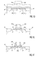
- this mask 13 After removing the resin mask 12 by oxygen plasma, we form, as shown on the Figure 1C in the case of the realization of the circuit integrated into different types of transistors, a new resin lithographic mask 13 defining the location of the source and drain of the transistors of a given type. To this end, this mask includes openings 15 opposite the regions 2a of the substrate in which must be made the transistors. In as part of the realization of CMOS circuits, this mask 13 is used in particular to mask the regions of the substrate intended for pMOS transistors.
- the n- implantation in the substrate can be carried out with phosphorus or arsenic at doses of 1x10 12 to 5x10 13 ions / cm 2 at energies of 50 to 100 keV.
- High-dose n + implantation in the silicon layer 8 can also be carried out with phosphorus or arsenic at doses of 1x10 14 to 1x10 15 ions / cm 2 (i.e. doses 20 to 100 times higher) and at energies from 10 to 25 keV; the implantation energies being directly linked to the implantation depth, the doping of the layer 8 is carried out with lower energies than those used for the doping of the substrate, for example from 4 to 5 times lower.
- the resin mask 13 is then removed by oxygen plasma.
- the implantation p- can be carried out with boron or BF + / 2 ions at the same doses as those used for n- implantation, but using energies from 10 to 70 keV. Then we perform p + implantation in layer 8 with ions of boron or BF + / 2 at the same doses as implantation n + in layer 8, but at energies from 10 to 50 keV. As for n-channel transistors, these p- and p + are performed using, in addition to the mask resin lithographic, a nitride mask of silicon produced at the same time as the mask 10a, masking the transistor channel in the same way as the mask 10a. This resin mask is removed after the p + implantation of layer 8.
- the first high dose implantation of the silicon layer 8 ensures doping of this layer up to the 8-6 silicon-oxide interface grid and in particular under the spacing strips or spacers made later (Figure 1E). This high dose doping of layer 8 also allows ensure proper high frequency operation of transistors.
- This layer 22 is in particular a layer of silicon oxide deposited by chemical phase deposition low pressure steam (LPCVD), this deposition technique ensuring the uniformity of the thickness of the layer 22. This thickness is approximately 100 to 200 nm. We obtain thus the structure shown in Figure 1D.
- LPCVD chemical phase deposition low pressure steam
- This engraving is of the type full plate engraving (i.e. without mask). She is performed in reactive ionic mode using a tri- or tetra-fluoromethane plasma for example.
- spacers 24 are voluntary residues resulting from oxide thicknesses on the sides of the mask 10a.
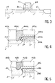
- a two-layer etching mask 10a In order to keep the mask 10a intact during the etching of the spacer strips 24, it is possible to use a two-layer etching mask 10a. This variant is shown in FIGS. 2 and 3. To this end, during the deposition of the layers intended to form the mask 10a, a layer 11 of Si 3 N 4 of 300 nm is deposited successively directly on the semiconductor layer 8 by LPCVD and a 30 nm SiO 2 layer 13 by low pressure chemical vapor deposition, by tetraethylorthosilicate pyrolysis (TEOS) or at low temperature (LTO).
- TEOS tetraethylorthosilicate pyrolysis
- LTO low temperature
- the two-layer etching mask 10a (FIG. 2) is produced as before by reactive ion etching using a plasma of tri- or tetrafluoromethane for the upper layer 13 in SiO 2 and a mixture of CHF 3 , C 2 F 6 for the lower layer 11 in Si 3 N 4 .
- the top layer 13 is made of a material of the same kind as that intended for spacers 24, the upper layer 13 is deleted, when engraving the spacers 24 (figure 3).
- the next step in the process consists in etching the semiconductor layer 8 so as to eliminate the regions not covered by the mask 10a but also by the spacers 24. This gives grid 8a of the transistors.
- This engraving must be selective in relation to to the spacing strips 24, to the side insulations 4 and compared to oxide 6, the latter also serving etching stop layer.
- This engraving of the layer 8 can be reactively ionized using a sulfur hexafluoride plasma for a silicon layer, this type of etching having high anisotropy characteristics.
- the etching of the silicon layer after the making spacers avoids etching on the surface of the field oxide 4.
- the oxide layer formed has a thickness of 10 to 20 nm.
- the next step in the process consists, as shown in Figure 1G, to be removed by etching anisotropic the oxide regions 6 exposed during the etching of the silicon layer 8.
- This elimination is carried out with a anisotropic dry etching with etching stop on the silicon substrate.
- This engraving is made from selectively compared to silicon, for example in using tri- or tetrafluoromethane. This removal of oxide above source regions and drain causes slight erosion of the spacers 24 and non-harmful field oxide (a few nm) the subsequent operation of the transistors and their subsequent manufacturing steps.
- the conductive epitaxy of a conductive layer 28 is carried out selectively over the regions. source and drain and on the grids 8a with respect to the field oxide 4, the spacers 24 and the lateral insulation 26 of the grids 8a.
- This layer 28 has a thickness of approximately 100 nm. It is in particular made of silicon with a high density of defects, that is to say quasi-amorphous or comprising micro-crystallines, so as to favor the formation of fine junctions, during the subsequent implantation, and this with good control of the depth of the joints; the epitaxy of silicon is obtained from the thermal decomposition of SiH 4 .
- Partial siliciding allows, as shown in FIG. 1G, obtaining a layer 29 of area. This layer reduces resistance of contact between layer 28 and the connections of the circuit.
- This layer 29 is obtained by siliciding self-positioned (or self-aligned) on the regions of source, drain and grid using metals of transition such as titanium or cobalt.
- This siliciding consists in depositing a metallic layer of Ti or Co on layer 28 and at heat the structure obtained between 500 and 800 ° C to that the metal reacts chemically with the silicon underlying and selectively removing the deposited metal elsewhere than on layer 28.
- An ion implantation 30 is then carried out in the layers 28 and 29 but also in the underlying source and drain regions and in the grids 8a.
- This implantation is a high dose implantation, that is to say that the dose is 10 to 50 times higher than that of the low dose implantation of the source and drain regions.
- phosphorus or arsenic ions are implanted at doses of 5 ⁇ 10 14 to 5 ⁇ 10 15 ions / cm 2 with an energy of 15 to 80 keV.
- n + implementation is carried out as previously using a mask 31, identical to mask 13, having openings 33 facing the n channel transistors to be produced and masking the rest of the circuit and in particular the regions in which must be made of transistors p channel for CMOS integrated circuits.
- the high dose implantation 30 is performed in using, in addition to the resin masks, the spacers 24 and the lateral insulations 26 of the grids 8a as mask, thus making it possible to physically separate the n + (respectively p +) source and drain regions 32 and 34 of the transistor channel.
- the last implanted ions are essentially located in the epitaxial layer of silicon 28 and the silicide layer 29. Also, for ensure diffusion of these ions in the substrate by view of the source 32 and drain 34 regions of type n +, and in the gate 8a of the transistors thus that an activation of the implanted ions, we perform a annealing of the structure obtained; this annealing is done either in the oven at 900 ° C for 2 to 3 tens of minutes under a nitrogen atmosphere, either by annealing fast by means of lamps.
- layer 28 epitaxial and implanted serves as a source of dopant for the grids and the source and drain regions of transistors.
- n + zones (respectively p +) physically embedded in zones n- (respectively p-) and suspended above the level of the transistor channel which is at the level of the regions n- (respectively p-) of transistors.
- the next step in the process consists in depositing a conductive layer 38 selectively on the silicide layer 29 with respect to the spacing strips 24, as shown in FIG. 1H, allowing the shunts of the grid, of the source and of the drain of each transistor.
- This conductive layer 38 is in particular tungsten deposited by LPCVD, at low temperature, by decomposition of WF 6 and SiH 4 , as described in the article by VV Lee cited above.
- This conductive layer 38 has a thickness of approximately 100 nm.
- Grid shunts, springs and drains obtained have a low resistance, of the order of 0.5 to 2 ohms / square.
- the MOS transistors thus obtained can withstand high supply voltages and particular of 5 V for 8a grids of 300 nm of large.
- isolation 40 in particular silicon oxide, on the whole structure. Creep leveling of this layer 40 can possibly be produced to soften the passage of metallization subsequent grids and interconnections of source and drain regions of circuit transistors integrated.
- openings 42 in the insulation layer 40 by reactive ion etching using a mask layer 38 serving as a barrier layer to this engraving.
- a mask layer 38 serving as a barrier layer to this engraving.
- conductive material 44 The presence of the conductive layer 38 facilitates the making contact at the bottom of the contact holes 42.
- the shunt layer provides a good seed for the growth of the metallization layer 44.
- This conductive material 44 is in particular selectively deposited as the conductive layer 38.
- the material 44 can be a silicide formed by local siliciding of the layer 38 or a metal. In the latter case, we use in particular tungsten deposited at low temperature by LPCVD as described in the article by V.V Lee cited above.
- FIGS. 4 and 5 represent extreme situations of making electrical contact on the source and drain regions of the transistors using the method according to the invention.
- the circuit elements have the same references as above, supplemented by the letters a and b respectively.
- contact electric is provided via the epitaxial layers 28a, 28b silicon, 29a or 29b silicide and 38a or 38b of shunt.
- the shunt layers 38a marry perfectly the contours of layer 29a and by therefore those of the conductive layer 28a, which thus constitutes a good protection of the diodes of source and drain at the edge of field oxide 4a or 4b.
- the stacking of these layers allows the realization of contacts 44a and 44b overflowing, without having to use a step additional and in particular an implantation ionic inside the contact holes 42a and 42b, formed respectively in the isolation layer 40a and 40b.
Landscapes
- Metal-Oxide And Bipolar Metal-Oxide Semiconductor Integrated Circuits (AREA)
- Insulated Gate Type Field-Effect Transistor (AREA)
Claims (11)
- Verfahren zur Herstellung einer integrierten Schaltung auf einem Halbleitersubstrat mit MIS-Transistoren, deren Sources (18, 32) und Drains (20, 34) aus doppelten Übergängen bestehen und deren Gates in einer Halbleiterschicht ausgebildet sind, eine erste Implantation (14) von Ionen eines bestimmten Konduktivitätstyps in das Substrat umfassend, mit einer bestimmten Dosis, um dort erste Source- und Drainübergänge (18 und 20) zu bilden, dann eine zweite Ionenimplantation (30) desselben Typs wie die erste, mit einer höheren Dosis als die erste Implantation, um die genannten doppelten Übergänge zu bilden, wobei dieses Verfahren die folgenden Schritte umfaßt:a) - Herstellen seitlicher elektrischer Isolationen (4) der Transistoren in dem genannten Substrat,b) - Abscheiden einer Schicht eines ersten Isolators (6) wenigstens zwischen den seitlichen Isolationen auf dem genannten Substrat,c) - Abscheiden - auf der in b) erhaltenen Struktur - einer Halbleiterschicht (8), die geeignet ist, dotiert und selektiv geätzt zu werden in bezug auf die genannten seitlichen Isolationen, den ersten Isolator und herzustellende isolierende Abstandsstreifen (24),d) - Herstellen - auf der Halbleiterschicht - einer Maske (10a), aus wenigstens einem Material, das geeignet ist, selektiv geätzt zu werden in bezug auf die genannten seitlichen Isolationen, den erste Isolator, die Halbleiterschicht, ein zweites isolierendes Material (26) und die genannten herzustellenden isolierenden Abstandsstreifen (24), die die Gates der herzuszellenden Transistoren in der Halbleiterschicht maskieren,e) - erste Ionenimplantation (14) in die Halbleiterschicht (8) und in das unmaskierte Substrat (2), um die ersten Source- und Drainübergänge (18 und 20) der Transistoren zu bilden,f) - Herstellen der genannten isolierenden Abstandsstreifen (24) auf den Flanken der Maske (10a),g) - Ätzen der Halbleiterschicht (8), um ihre nicht durch die Maske abgedeckten Bereiche zu eliminieren und die genannten isolierenden Abstandsstreifen sowie das Gate 8a des Transistors bilden,h) - Isolieren der geätzten Flanken der Halbleiterschicht mit dem zweiten Isolator (26),i) - Eliminieren der Maske (10a) durch selektives Ätzen in bezug auf die genannten seitlichen Isolationen (4), die Schicht des ersten Isolators (6), die Halbleiterschicht (8), die Isolation der geätzten Flanken, und in bezug auf die genannten Abstandsstreifen (24),j) - Eliminieren der in Schritt g) freigelegten Bereiche des ersten Isolators durch selektives Ätzen in bezug auf die Halbleiterschicht (8) und in bezug auf das Substrat,k) - Abscheiden einer leitenden Schicht (28) mittels einer Epitaxietechnik auf den Bereichen der Source (18) und des Drains (20), freigelegt in Schritt j), und auf dem Gate (8a) der Transistoren, selektiv in bezug auf die genannten seitlichen Isolationen (4), die genannten Abstandsstreifen (24) und in bezug auf die Isolation (26) der geätzten Flanken,l) - zweite Ionenimplantation (30) in die leitende Schicht (28) und in die Source- und Drainbereiche, damit dort die doppelten Übergänge teilweise gebildet werden,m) - Herstellen der elektrischen Verbindungen der integrierten Schaltung.
- Verfahren nach Anspruch 1, dadurch gekennzeichnet, daß man zwischen den Schritten 1) und m) auf der leitenden Schicht (28) ein leitendes Material (38) abscheidet, selektiv in bezug auf den genannten Abstandstreifen, den genannten seitlichen Isolationen und dem zweiten Isolator, um die Shunts bzw. Nebenschlüsse der Gates, der Sources und der Drains zu bilden.
- Verfahren nach Anspruch 2, dadurch gekennzeichnet, daß man zwischen der leitenden Schicht (28) und dem leitenden Material (38) auf dieser Schicht (28) eine leitende Zwischenschicht (29) abscheidet, selektiv in bezug auf die Abstandsstreifen, die seitlichen Isolationen und den zweiten Isolator.
- Verfahren nach einem der vorangehenden Ansprüche, dadurch gekennzeichnet, daß die Maske (10a) durch eine Aufeinanderschichtung von zwei Materialien (13, 11) gebildet wird, wobei das direkt auf der Halbleiterschicht (8) gebildete Material (11) selektiv geätzt werden kann in bezug auf den ersten Isolator, die Halbleiterschicht, das zweite isolierende Material (26), die genannten isolierenden Abstandsstreifen und die seitlichen Isolationen.
- Verfahren nach einem der vorangehenden Ansprüche, dadurch gekennzeichnet, daß der Schritt m) darin besteht, auf der gesamten in l) erhaltenen Struktur eine Isolierschicht (40) abzuscheiden; in dieser Isolierschicht gegenüber den anzuschließenden Gates (8a), Sources (18, 32) und Drains (20, 34) Kontaktlöcher (42) zu bilden; in den Kontaktlöchern (42) in bezug auf die Isolierschicht (40) selektiv ein leitendes Material (44) abzuscheiden.
- Verfahren nach einem der Ansprüche 2 bis 5, dadurch gekennzeichnet, daß das selektiv auf der leitenden Schicht abgeschiedene Material und/oder das in den Kontaktlöchern abgeschiedene Material mittels LPCVD abgeschiedenes Wolfram, Silicium, ein Silicid oder ein unter Platin, Palladium und Kupfer ausgewähltes Metall ist.
- Verfahren nach einem der vorangehenden Ansprüche, dadurch gekennzeichnet, daß die Maske (10a) durch eine Si3N4-Schicht (11) und eine SiO2-Schicht (13) gebildet wird, wobei die Si3N4-Schicht direkt auf der Halbleiterschicht gebildet wird.
- Verfahren nach einem der vorangehenden Ansprüche, dadurch gekennzeichnet, daß man nach der zweiten Implantation ein Tempern der Schaltung durchführt, damit die implantierten Ionen diffundieren und aktiviert werden.
- Verfahren nach einem der vorangehenden Ansprüche, dadurch gekennzeichnet, daß das Substrat (2), die Halbleiterschicht (8) und die leitende Schicht (28) aus Silicium sind.
- Verfahren nach einem der vorangehenden Ansprüche, dadurch gekennzeichnet, daß das Substrat (2) und die Halbleiterschicht (8) aus Silicium sind, und dadurch, daß die leitende Schicht (28) wenigstens teilweise durch ein Silicid eines Übergangsmetalls gebildet wird.
- Verfahren nach Anspruch 10, dadurch gekennzeichnet, daß das Übergangsmetall Titan oder Kobalt ist.
Applications Claiming Priority (2)
| Application Number | Priority Date | Filing Date | Title |
|---|---|---|---|
| FR8912697 | 1989-09-28 | ||
| FR8912697A FR2652448B1 (fr) | 1989-09-28 | 1989-09-28 | Procede de fabrication d'un circuit integre mis haute tension. |
Publications (2)
| Publication Number | Publication Date |
|---|---|
| EP0420748A1 EP0420748A1 (de) | 1991-04-03 |
| EP0420748B1 true EP0420748B1 (de) | 1999-01-27 |
Family
ID=9385899
Family Applications (1)
| Application Number | Title | Priority Date | Filing Date |
|---|---|---|---|
| EP90402651A Expired - Lifetime EP0420748B1 (de) | 1989-09-28 | 1990-09-26 | Verfahren zur Herstellung einer Hochspannungs-MIS-integrierten Schaltung |
Country Status (6)
| Country | Link |
|---|---|
| US (1) | US5314832A (de) |
| EP (1) | EP0420748B1 (de) |
| JP (1) | JP3038862B2 (de) |
| CA (1) | CA2026126A1 (de) |
| DE (1) | DE69032917T2 (de) |
| FR (1) | FR2652448B1 (de) |
Cited By (1)
| Publication number | Priority date | Publication date | Assignee | Title |
|---|---|---|---|---|
| US7338874B2 (en) | 2003-08-22 | 2008-03-04 | Samsung Electronics Co., Ltd. | Highly integrated semiconductor device with silicide layer that secures contact margin and method of manufacturing the same |
Families Citing this family (33)
| Publication number | Priority date | Publication date | Assignee | Title |
|---|---|---|---|---|
| JPH0555250A (ja) * | 1991-08-28 | 1993-03-05 | Rohm Co Ltd | 半導体装置およびその製法 |
| JPH05110005A (ja) * | 1991-10-16 | 1993-04-30 | N M B Semiconductor:Kk | Mos型トランジスタ半導体装置およびその製造方法 |
| US5429987A (en) * | 1993-01-25 | 1995-07-04 | Sharp Microelectronics Technology, Inc. | Method for profile control of selective metallization |
| US5672530A (en) * | 1993-03-22 | 1997-09-30 | Sharp Microelectronics Technology, Inc. | Method of making MOS transistor with controlled shallow source/drain junction |
| JP3181773B2 (ja) * | 1993-10-29 | 2001-07-03 | シャープ株式会社 | 半導体装置の製造方法 |
| US5671397A (en) * | 1993-12-27 | 1997-09-23 | At&T Global Information Solutions Company | Sea-of-cells array of transistors |
| US5472895A (en) * | 1993-12-27 | 1995-12-05 | Hyundai Electronics Industries Co., Ltd. | Method for manufacturing a transistor of a semiconductor device |
| US6675361B1 (en) * | 1993-12-27 | 2004-01-06 | Hyundai Electronics America | Method of constructing an integrated circuit comprising an embedded macro |
| JPH0837164A (ja) * | 1994-07-21 | 1996-02-06 | Nec Corp | 半導体装置の製造方法 |
| US5496750A (en) * | 1994-09-19 | 1996-03-05 | Texas Instruments Incorporated | Elevated source/drain junction metal oxide semiconductor field-effect transistor using blanket silicon deposition |
| JP3426043B2 (ja) * | 1994-09-27 | 2003-07-14 | 株式会社半導体エネルギー研究所 | 半導体装置の作製方法 |
| US5824577A (en) * | 1995-02-16 | 1998-10-20 | National Semiconductor Corporation | MOSFET with reduced leakage current |
| KR100206878B1 (ko) * | 1995-12-29 | 1999-07-01 | 구본준 | 반도체소자 제조방법 |
| EP0813234A3 (de) * | 1996-06-12 | 1999-05-26 | Texas Instruments Incorporated | Verfahren zur Herstellung eines MOSFETS |
| US5824586A (en) * | 1996-10-23 | 1998-10-20 | Advanced Micro Devices, Inc. | Method of manufacturing a raised source/drain MOSFET |
| US6046471A (en) * | 1996-11-07 | 2000-04-04 | Advanced Micro Devices, Inc. | Ultra shallow junction depth transistors |
| US5780349A (en) * | 1997-02-20 | 1998-07-14 | National Semiconductor Corporation | Self-aligned MOSFET gate/source/drain salicide formation |
| DE19718167C1 (de) * | 1997-04-29 | 1998-06-18 | Siemens Ag | MOS-Transistor und Verfahren zu dessen Herstellung |
| US6518155B1 (en) | 1997-06-30 | 2003-02-11 | Intel Corporation | Device structure and method for reducing silicide encroachment |
| US6777759B1 (en) | 1997-06-30 | 2004-08-17 | Intel Corporation | Device structure and method for reducing silicide encroachment |
| US6610564B2 (en) * | 2000-03-03 | 2003-08-26 | Shinichi Fukada | Method of fabricating semiconductor device |
| US5940698A (en) * | 1997-12-01 | 1999-08-17 | Advanced Micro Devices | Method of making a semiconductor device having high performance gate electrode structure |
| US5837588A (en) * | 1998-01-26 | 1998-11-17 | Texas Instruments-Acer Incorporated | Method for forming a semiconductor device with an inverse-T gate lightly-doped drain structure |
| JP2000156502A (ja) * | 1998-09-21 | 2000-06-06 | Texas Instr Inc <Ti> | 集積回路及び方法 |
| US6211026B1 (en) | 1998-12-01 | 2001-04-03 | Micron Technology, Inc. | Methods of forming integrated circuitry, methods of forming elevated source/drain regions of a field effect transistor, and methods of forming field effect transistors |
| US6211048B1 (en) * | 1998-12-21 | 2001-04-03 | United Microelectronics Corp. | Method of reducing salicide lateral growth |
| US6660600B2 (en) | 2001-01-26 | 2003-12-09 | Micron Technology, Inc. | Methods of forming integrated circuitry, methods of forming elevated source/drain regions of a field effect transistor, and methods of forming field effect transistors |
| DE10103524A1 (de) * | 2001-01-26 | 2002-08-22 | Infineon Technologies Ag | Verfahren und Halbleiteranordnung zur Ätzung einer Schicht eines Halbleitersubstrats mittels einer siliziumhaltigen Ätzmaske |
| JP2005531158A (ja) * | 2002-06-26 | 2005-10-13 | セムエキップ インコーポレイテッド | 半導体デバイス及び半導体デバイスの製造方法 |
| US20080200020A1 (en) * | 2003-06-18 | 2008-08-21 | Semequip, Inc. | Semiconductor device and method of fabricating a semiconductor device |
| US7012024B2 (en) * | 2003-08-15 | 2006-03-14 | Micron Technology, Inc. | Methods of forming a transistor with an integrated metal silicide gate electrode |
| JP2010067748A (ja) * | 2008-09-10 | 2010-03-25 | Rohm Co Ltd | 半導体装置および半導体装置の製造方法 |
| JP5220549B2 (ja) * | 2008-10-20 | 2013-06-26 | 本田技研工業株式会社 | アウタロータ型多極発電機のステータ構造体 |
Family Cites Families (6)
| Publication number | Priority date | Publication date | Assignee | Title |
|---|---|---|---|---|
| US4569122A (en) * | 1983-03-09 | 1986-02-11 | Advanced Micro Devices, Inc. | Method of forming a low resistance quasi-buried contact |
| JPS60117719A (ja) * | 1983-11-30 | 1985-06-25 | Fujitsu Ltd | 半導体装置の製造方法 |
| JPS62221158A (ja) * | 1986-03-24 | 1987-09-29 | Toshiba Corp | 半導体装置の製造方法 |
| JPH01265541A (ja) * | 1988-04-15 | 1989-10-23 | Fujitsu Ltd | 半導体装置 |
| US5079180A (en) * | 1988-12-22 | 1992-01-07 | Texas Instruments Incorporated | Method of fabricating a raised source/drain transistor |
| US5168072A (en) * | 1990-10-12 | 1992-12-01 | Texas Instruments Incorporated | Method of fabricating an high-performance insulated-gate field-effect transistor |
-
1989
- 1989-09-28 FR FR8912697A patent/FR2652448B1/fr not_active Expired - Fee Related
-
1990
- 1990-09-25 CA CA002026126A patent/CA2026126A1/en not_active Abandoned
- 1990-09-26 EP EP90402651A patent/EP0420748B1/de not_active Expired - Lifetime
- 1990-09-26 DE DE69032917T patent/DE69032917T2/de not_active Expired - Fee Related
- 1990-09-28 JP JP2257627A patent/JP3038862B2/ja not_active Expired - Lifetime
-
1992
- 1992-02-12 US US07/835,106 patent/US5314832A/en not_active Expired - Fee Related
Cited By (1)
| Publication number | Priority date | Publication date | Assignee | Title |
|---|---|---|---|---|
| US7338874B2 (en) | 2003-08-22 | 2008-03-04 | Samsung Electronics Co., Ltd. | Highly integrated semiconductor device with silicide layer that secures contact margin and method of manufacturing the same |
Also Published As
| Publication number | Publication date |
|---|---|
| EP0420748A1 (de) | 1991-04-03 |
| FR2652448B1 (fr) | 1994-04-29 |
| FR2652448A1 (fr) | 1991-03-29 |
| US5314832A (en) | 1994-05-24 |
| JPH03120837A (ja) | 1991-05-23 |
| CA2026126A1 (en) | 1991-03-29 |
| DE69032917D1 (de) | 1999-03-11 |
| JP3038862B2 (ja) | 2000-05-08 |
| DE69032917T2 (de) | 1999-07-29 |
Similar Documents
| Publication | Publication Date | Title |
|---|---|---|
| EP0420748B1 (de) | Verfahren zur Herstellung einer Hochspannungs-MIS-integrierten Schaltung | |
| EP0426250B1 (de) | Verfahren zur Herstellung eines MIS-Transistor-Bauelementes mit einem Gitter, welches über geringdotierte Teile der Source- und Drain-Gebiete herausragt | |
| EP0443958B1 (de) | Verfahren zum Herstellen einer analogen integrierten Hochgeschwindigkeitsschaltung unter Verwendung von lokalen Leitungsverbindungen aus Silizid | |
| EP0462882A1 (de) | Dünnfilm-Feldeffekttransistor mit vergrabenem Gate und Verfahren zur Herstellung | |
| EP0164281A1 (de) | Verfahren zur Herstellung einer vergrabenen Isolierschicht in einem Halbleitersubstrat durch Ionenimplantation | |
| EP0426251A1 (de) | Verfahren zur Herstellung eines MIS-Transistor-Bauelementes mit einer invertierten T-förmigen Gitterelektrode | |
| FR2530867A1 (fr) | Dispositifs mos a barriere de schottky et leur procede de fabrication | |
| FR2806832A1 (fr) | Transistor mos a source et drain metalliques, et procede de fabrication d'un tel transistor | |
| EP2323160A1 (de) | Verfahren zur Herstellung von Feldeffekttransistoren mit einer Gegenelektrode und Halbleitervorrichtung | |
| FR2756102A1 (fr) | Dispositif a semi-conducteur commande par une grille mos et procede pour sa fabrication | |
| FR2757312A1 (fr) | Transistor mis a grille metallique auto-alignee et son procede de fabrication | |
| EP0463972A1 (de) | Verfahren zum Herstellen eines elektrischen Kontakts auf dem aktiven Element einer MIS-integrierten Schaltung | |
| WO2000046858A1 (fr) | Transistor mos a tension de seuil dynamique equipe d'un limiteur de courant, et procede de realisation d'un tel transistor | |
| EP0635880B1 (de) | Verfahren zur Herstellung eines Transistors in Silizium-auf-Isolator Technologie | |
| EP0414618B1 (de) | Dünnfilm-MOS-Transistor, bei dem die Kanalzone mit der Source verbunden ist, und Verfahren zur Herstellung | |
| EP0190243B1 (de) | Verfahren zur herstellung einer integrierten schaltung vom mis-typ | |
| EP0522938B1 (de) | Verfahren zum Herstellen eines vertikalen Feldeffekt-Transistors und durch dieses Verfahren hergestellter Transistor | |
| EP1006573A1 (de) | Herstellungsverfahren für integrierte BiCMOS Schaltkreise auf einem gewöhnlichen CMOS Substrat | |
| WO2002037560A1 (fr) | Procede de fabrication simultanee d"une paire de transistors a grilles isolees ayant respectivement un oxyde fin et un oxyde epais, et circuit integre correspondant comprenant une telle paire de transistors | |
| FR2864345A1 (fr) | Realisation de la peripherie d'une diode schottky a tranchees mos | |
| FR2648622A1 (fr) | Procede de fabrication d'un circuit integre comportant un transistor a effet de champ a double implantation | |
| EP1650796A2 (de) | Verfahren für einen Kontaktanschluss auf einer Region einer integrierten Schaltung, insbesondere auf Transistorelektroden | |
| FR2464561A1 (fr) | Structure de transistors complementaires (cmos) et son procede de fabrication | |
| FR3138242A1 (fr) | Procédé de fabrication de diode schottky et circuit intégré correspondant | |
| EP0194916B1 (de) | Verfahren zum Herstellen von integrierten Schaltungen durch MOS- und CMOS-Technologie und entsprechende CMOS-Struktur |
Legal Events
| Date | Code | Title | Description |
|---|---|---|---|
| PUAI | Public reference made under article 153(3) epc to a published international application that has entered the european phase |
Free format text: ORIGINAL CODE: 0009012 |
|
| AK | Designated contracting states |
Kind code of ref document: A1 Designated state(s): DE ES FR GB IT NL |
|
| 17P | Request for examination filed |
Effective date: 19910906 |
|
| 17Q | First examination report despatched |
Effective date: 19950307 |
|
| GRAG | Despatch of communication of intention to grant |
Free format text: ORIGINAL CODE: EPIDOS AGRA |
|
| GRAG | Despatch of communication of intention to grant |
Free format text: ORIGINAL CODE: EPIDOS AGRA |
|
| GRAH | Despatch of communication of intention to grant a patent |
Free format text: ORIGINAL CODE: EPIDOS IGRA |
|
| GRAH | Despatch of communication of intention to grant a patent |
Free format text: ORIGINAL CODE: EPIDOS IGRA |
|
| GRAA | (expected) grant |
Free format text: ORIGINAL CODE: 0009210 |
|
| AK | Designated contracting states |
Kind code of ref document: B1 Designated state(s): DE ES FR GB IT NL |
|
| PG25 | Lapsed in a contracting state [announced via postgrant information from national office to epo] |
Ref country code: NL Free format text: LAPSE BECAUSE OF FAILURE TO SUBMIT A TRANSLATION OF THE DESCRIPTION OR TO PAY THE FEE WITHIN THE PRESCRIBED TIME-LIMIT Effective date: 19990127 Ref country code: ES Free format text: THE PATENT HAS BEEN ANNULLED BY A DECISION OF A NATIONAL AUTHORITY Effective date: 19990127 |
|
| REF | Corresponds to: |
Ref document number: 69032917 Country of ref document: DE Date of ref document: 19990311 |
|
| ITF | It: translation for a ep patent filed | ||
| GBT | Gb: translation of ep patent filed (gb section 77(6)(a)/1977) |
Effective date: 19990401 |
|
| NLV1 | Nl: lapsed or annulled due to failure to fulfill the requirements of art. 29p and 29m of the patents act | ||
| PLBE | No opposition filed within time limit |
Free format text: ORIGINAL CODE: 0009261 |
|
| STAA | Information on the status of an ep patent application or granted ep patent |
Free format text: STATUS: NO OPPOSITION FILED WITHIN TIME LIMIT |
|
| 26N | No opposition filed | ||
| PGFP | Annual fee paid to national office [announced via postgrant information from national office to epo] |
Ref country code: GB Payment date: 20000920 Year of fee payment: 11 |
|
| PGFP | Annual fee paid to national office [announced via postgrant information from national office to epo] |
Ref country code: FR Payment date: 20000927 Year of fee payment: 11 |
|
| PGFP | Annual fee paid to national office [announced via postgrant information from national office to epo] |
Ref country code: DE Payment date: 20000928 Year of fee payment: 11 |
|
| PG25 | Lapsed in a contracting state [announced via postgrant information from national office to epo] |
Ref country code: GB Free format text: LAPSE BECAUSE OF NON-PAYMENT OF DUE FEES Effective date: 20010926 |
|
| REG | Reference to a national code |
Ref country code: GB Ref legal event code: IF02 |
|
| PG25 | Lapsed in a contracting state [announced via postgrant information from national office to epo] |
Ref country code: DE Free format text: LAPSE BECAUSE OF NON-PAYMENT OF DUE FEES Effective date: 20020501 |
|
| GBPC | Gb: european patent ceased through non-payment of renewal fee |
Effective date: 20010926 |
|
| PG25 | Lapsed in a contracting state [announced via postgrant information from national office to epo] |
Ref country code: FR Free format text: LAPSE BECAUSE OF NON-PAYMENT OF DUE FEES Effective date: 20020531 |
|
| REG | Reference to a national code |
Ref country code: FR Ref legal event code: ST |
|
| PG25 | Lapsed in a contracting state [announced via postgrant information from national office to epo] |
Ref country code: IT Free format text: LAPSE BECAUSE OF NON-PAYMENT OF DUE FEES;WARNING: LAPSES OF ITALIAN PATENTS WITH EFFECTIVE DATE BEFORE 2007 MAY HAVE OCCURRED AT ANY TIME BEFORE 2007. THE CORRECT EFFECTIVE DATE MAY BE DIFFERENT FROM THE ONE RECORDED. Effective date: 20050926 |