EP0607670B1 - Datenverrieglung - Google Patents
Datenverrieglung Download PDFInfo
- Publication number
- EP0607670B1 EP0607670B1 EP93309671A EP93309671A EP0607670B1 EP 0607670 B1 EP0607670 B1 EP 0607670B1 EP 93309671 A EP93309671 A EP 93309671A EP 93309671 A EP93309671 A EP 93309671A EP 0607670 B1 EP0607670 B1 EP 0607670B1
- Authority
- EP
- European Patent Office
- Prior art keywords
- data
- bus
- signal
- valid
- circuit
- Prior art date
- Legal status (The legal status is an assumption and is not a legal conclusion. Google has not performed a legal analysis and makes no representation as to the accuracy of the status listed.)
- Expired - Lifetime
Links
Images


Classifications
-
- G—PHYSICS
- G06—COMPUTING OR CALCULATING; COUNTING
- G06F—ELECTRIC DIGITAL DATA PROCESSING
- G06F13/00—Interconnection of, or transfer of information or other signals between, memories, input/output devices or central processing units
- G06F13/38—Information transfer, e.g. on bus
- G06F13/40—Bus structure
- G06F13/4063—Device-to-bus coupling
- G06F13/4068—Electrical coupling
- G06F13/4072—Drivers or receivers
- G06F13/4077—Precharging or discharging
-
- Y—GENERAL TAGGING OF NEW TECHNOLOGICAL DEVELOPMENTS; GENERAL TAGGING OF CROSS-SECTIONAL TECHNOLOGIES SPANNING OVER SEVERAL SECTIONS OF THE IPC; TECHNICAL SUBJECTS COVERED BY FORMER USPC CROSS-REFERENCE ART COLLECTIONS [XRACs] AND DIGESTS
- Y02—TECHNOLOGIES OR APPLICATIONS FOR MITIGATION OR ADAPTATION AGAINST CLIMATE CHANGE
- Y02D—CLIMATE CHANGE MITIGATION TECHNOLOGIES IN INFORMATION AND COMMUNICATION TECHNOLOGIES [ICT], I.E. INFORMATION AND COMMUNICATION TECHNOLOGIES AIMING AT THE REDUCTION OF THEIR OWN ENERGY USE
- Y02D10/00—Energy efficient computing, e.g. low power processors, power management or thermal management
Definitions
- the present invention as it is defined in the appended claims relates to data caching in digital circuits and may provide power saving features in precharged bus circuitry.
- a precharged bus is a bus operated in conjunction with a multi-phase clock, on which data may be driven during a data-drive phase, and which is precharged to a precharge level (i.e., VDD) during a precharge phase.
- VDD precharge level
- US-A-5 093 588 discloses a system including a precharge bus design.
- precharge signals may be conducted to the receiving circuit through a latch that is enabled before the precharged bus is driven with valid data.
- the receiving circuit may receive precharge signals in a data-drive phase during which no data is to be driven on the precharged bus. The propagation of precharge signals through the receiving circuit, "precharge rippling", may result in unnecessary transitions and invalid data at the output of the receiving circuit. The unnecessary transitions cause excess power consumption and additional noise.
- the latch circuit includes an input line for receiving data from the bus, a latch for conducting electrical signals from the bus to the receiving circuit, and a structure for enabling the latch only when data is being driven on the bus during a data-drive phase.
- the structure for enabling may include a data-clock signal that indicates a data-drive phase, a data-valid signal that is asserted when data is driven on the bus and a control circuit responsive to the data-valid signal and the data-clock signal, the control circuit for delaying the enabling of the latch during a data-drive phase until data is driven on the bus.
- the data-valid signal may possess the same timing as the data driven on the bus, and in some embodiments of the present invention may be conducted on an extra line of the bus.
- the extra line may be driven by a circuit of the same design as the circuit used to drive the data lines of the bus, and may also have the same loading as the data lines.
- an enable signal which enables data to be driven onto the data lines may also be used to enable the assertion of the data-valid signal on the extra line.
- the latch circuit also includes a structure for delaying the enabling of the latch until some time after data is driven onto the bus.
- the structure may include at least one inverter connected in series between the extra line carrying the data-valid signal and the control circuit input.
- an apparatus for controlling the receiving of data by a receiving circuit from a precharged bus including an input line for receiving data from the precharged bus, a latch for conducting electrical signals from the input line to the receiving circuit, and an enabling means for enabling the latch such that precharge values are not conducted to the receiving circuit.
- This method includes the steps of indicating when data may be driven onto the bus, generating a data-valid signal that is asserted only when data is driven onto the bus, and latching electrical signals from the bus to the receiving circuit only when data may be driven onto the bus and the data-valid signal is asserted.
- the method provided by the invention includes the steps of generating a data-clock signal that indicates the timing of data-drive phases and precharge phases, asserting an indicator signal when data is being driven on the precharged bus, combining the data-clock signal and the indicator signal into an enable signal, the enable signal being asserted when data is being driven on the precharged bus during a data-drive phase, and enabling the conduction of electrical signals from the precharged bus to the receiving circuit only when the enable signal is asserted.
- FIG. 1 an example of one bit line of a precharged data bus as is generally known to those skilled in the art of logic design.
- the bit line 2 consists of a data line 4 , a pull-up transistor 6 , and a bus driver 8 for each source of data.
- Each driver 8 has two transistors 10 and 12 in series.
- the precharged data bus operates in conjunction with a multi-phase clock such that the bus may be precharged (i.e., pulled to a high level) during a precharge phase, and may be driven with data during a data-drive phase.
- the gate of pull-up transistor 6 is connected to a precharge phase indicator (shown in FIG.
- the gate of transistor 10 receives a data-drive phase indicator (shown in FIG. 1 as ⁇ d ) ANDed with a driver enabling signal (ENABLEn) such that transistor 10 is turned on during a data-drive phase if that particular driver has been enabled.
- the gate of transistor 12 receives the data to be driven (DATAn) such that transistor 12 is turned on if the data is TRUE, and is turned off if the data is FALSE.
- DATAn data to be driven
- the precharged bus in FIG. 1 uses negative logic. If the data is TRUE, the bus is pulled to a low level (VSS). If the data is FALSE, the bus is tri-stated and retains its precharge value of VDD.
- the drivers required for such a precharged bus need only include two series transistors.
- a non-precharged bus typically requires the driver from each source of data to include a sourcing transistor, a sinking transistor, and a method for disabling both transistors.
- the use of a precharged bus reduces the number of transistors needed in the driver for each source of data and, therefore, reduces the design cost.
- FIG. 2 Shown in FIG. 2 is an example of a precharged bus used in conjunction with a receiving circuit.
- the example includes data line 4 of a precharged bus, a latch 20 , and an asynchronous logic 22 as a receiving circuit.
- the data line 4 is connected to the input of latch 20 .
- the gate of latch 20 is controlled by the DATA CLOCK signal which is high during each data-drive phase and low during each precharge phase.
- the output of latch 20 is conducted on line 28 and received as LOGIC INPUT by the asynchronous logic 22 .
- the asynchronous logic 22 In response to LOGIC INPUT, the asynchronous logic 22 generates a LOGIC OUTPUT on line 24 .
- DATA CLOCK When DATA CLOCK is low, the latch 20 is disabled and the signal on data line 4 is not received by the asynchronous logic 22 . When DATA CLOCK is high, latch 20 is enabled and allows the signal on data line 4 to pass through the latch 20 and be received by the asynchronous logic 22 . It should be noted here that DATA CLOCK indicates when data may be driven on the bus, but does not necessarily indicate that data is being driven on the bus. During any particular data-drive phase, data is usually not driven on the bus until some time after the low-to-high transition of DATA CLOCK. During the time that DATA CLOCK is high and before data is driven onto the bus, the bus remains at its precharge level.
- the precharge signal conducted on data line 4 may be latched into and propagate through the asynchronous circuit.
- This precharge rippling may cause unnecessary transistor switching in the asynchronous circuit and may therefore cause excess power consumption and additional noise. Also, the precharge rippling may cause invalid data to appear as LOGIC OUTPUT on line 24 .
- DATA CLOCK is driven high during the data-drive phase (indicated by ⁇ d ) and low during the precharge phase (indicated by ⁇ p ).
- the data bus is precharged to a high level (VDD).
- VDD high level
- a data source may drive data onto the data line 4 , which data may be latched into functional blocks such as the asynchronous logic 22 shown in FIG. 2 , and used for operation or calculation by that functional block.
- a low signal is driven on the data line 4 and ripples through the asynchronous logic 22 resulting in a change in LOGIC OUTPUT on line 24 .
- the asynchronous logic and its output then remains unchanged until time t 0 when DATA CLOCK is driven high enabling latch 20 .
- DATA CLOCK enables latch 20 while the data bus still retains its precharge value
- the input to the asynchronous logic 22 transitions from low to high at time t 0 .
- the precharge value then propagates through the asynchronous logic. This precharge rippling may result in the switching of transistors within the asynchronous logic and a change in LOGIC OUTPUT shown in FIG. 3 as occurring at time t 1 .
- Valid data does not appear as LOGIC INPUT until time t 2 , after which time the valid data propagates through the asynchronous logic resulting in a correct LOGIC OUTPUT at time t 3 .
- the switching of transistors within the asynchronous logic from the time the precharge value is received (t 0 ), until the time the valid data is received (t 2 ) is unnecessary and results in excess power consumption.
- the value appearing as LOGIC OUTPUT between times t 1 and t 3 is a result of the precharge rippling and may be invalid.
- Another instance of undesirable precharge rippling may occur when no data is driven onto the data bus during a data-drive phase, as shown in the period TP5 in FIG. 3 .
- the asynchronous logic has responded to the data that was driven during TP3.
- latch 20 is enabled by DATA CLOCK going high, and the precharge value is received by and ripples through the asynchronous logic 22 which may cause LOGIC OUTPUT to change at time t 5 .
- This change in the asynchronous logic 22 is also unnecessary and power consuming, and results in invalid data appearing as LOGIC OUTPUT.
- precharged bus decreases the amount of circuitry required.
- the use of a precharged bus can result in precharge rippling through a receiving circuit such as asynchronous logic 22 which increases power consumption and results in invalid data appearing at the output of the receiving circuit.
- the precharged bus may utilize any multi-phase clock.
- FIG. 4 Shown in FIG. 4 is an example of a latch circuit 30 designed in accordance with the principles of the present invention for delaying the latching of signals from a precharged bus to a receiving circuit, thereby preventing the latching of precharge signals which causes undesirable precharge rippling.
- Data from the precharged data bus is conducted on data line 4 .
- Latch 20 has an input connected to data line 4 and an output connected to a receiving circuit, labeled in FIG. 4 as asynchronous circuit 22 .
- the gate of latch 20 is connected to the output of a structure for enabling the latch so that precharge values are not conducted from the precharged bus to the asynchronous circuit 22 .
- the structure for enabling includes an AND gate 32 having an input line 34 carrying a DATA CLOCK signal, an input line 36 carrying a DATA VALID signal, and an output connected to the gate of latch 20 .
- the DATA VALID signal is the output of inverter 38 which receives the DATA VALID signal. The function of inverter 38 will be explained subsequently.
- the DATA CLOCK signal indicates when the precharged bus is in a data-drive phase and when it is in a precharge phase.
- DATA CLOCK is high during data-drive phases, and low during precharge phases.
- the DATA VALID signal indicates when data is being driven on the bus.
- DATA VALID is low only when data is driven on the precharged bus.
- the inverted DATA VALID signal and the DATA CLOCK signal are received by AND gate 32 such that the output of the AND gate is high only if the precharged bus is in a data-drive phase and data is being driven on the precharged bus.
- the latch circuit of the present invention prevents the receiving of precharge values from the precharged bus to a receiving circuit such as the asynchronous logic 22 .
- the DATA VALID signal be received from an extra line 40 added to the precharged bus.
- the extra line 40 may be driven by a circuit of the same design as the circuits used to drive the data lines 42 .
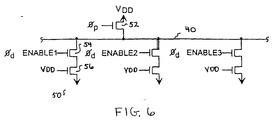
- the extra line may be driven by a circuit of the same design as is shown in FIG. 6 .
- the extra line 40 may be driven by a driver 50 or may be pulled up to VDD by pull-up transistor 52 . As was the case with the circuit shown in FIG.
- the gate of pull-up transistor 52 is connected to a precharge phase indicator such that pull-up transistor 52 turns on and pulls the extra line 40 up to VDD during every precharge phase.
- Each driver 50 includes a transistor 54 and transistor 56 in series.
- the gate of transistor 12 is tied to VDD.
- the gate of transistor 54 is controlled by a data-phase indicator ANDed with a driver enabling signal (ENABLEn) such that transistor 54 is turned on during a data-drive phase if that particular driver has been enabled.
- ENABLEn tied to the gate of transistor 54 is the same ENABLEn signal as was shown in FIG. 1 .
- the assertion of the ENABLEn signal causes the DATA SOURCEn signal of FIG.
- the extra line 40 carrying the DATA VALID signal have a loading similar to the loading of the other lines of the precharged bus. Because the data lines 42 and the extra line 40 have similar loading, the timing of the data and the DATA VALID signal will be the same. Thus, the assertion of DATA VALID will be received by latch circuit 30 at the same time that it receives valid data, thereby reducing the chance of latching precharge value, instead of valid data, into the receiving circuit.
- the latch circuit of the present invention may also include a structure for further delaying the latching of data from the precharged data bus to the asynchronous circuit.
- This structure for further delaying may include at least one inverter 38 having an input connected the extra line 40 of the precharged bus and having an output connected to the AND gate 32 .
- the inverter 38 delays the conduction of the DATA VALID signal to the input of the AND gate which, in turn, delays the low to high transition at the output of the AND gate 32 .
- the enabling of latch 20 is further delayed from the time that valid data appears on data line 4 until the DATA VALID signal propagates through inverter 38 and AND gate 32 . This delay allows for further assurance that only valid data will be received by the asynchronous logic.
- the latch circuit embodying the present invention includes a input line such as data line 4 , a latch connected between the input line and a receiving circuit, and a structure for enabling the latch such that precharge values are not conducted to the receiving circuit.
- the structure for enabling the latch may include an indicator signal for indicating when the precharged bus is being driven with data, a data clock signal for indicating data-drive phases, and a logic circuit that receives the indicator signal and the data clock signal and that generates an output that is asserted when the precharged bus is being driven with data during a data-drive phase.
- the indicator signal may be a DATA VALID signal conducted on an extra line 40 added to the precharged bus.
- the extra line 40 has the same loading as the other data lines 42 of the precharged bus.
- the logic circuit may be an AND gate 32 .
- the latch circuit of the present invention may include at least one inverter 38 connected between the extra line 40 and the AND gate 32 providing a delay between the time DATA VALID is asserted and the time DATA VALID is received by the AND gate 32 .
- the timing diagram shown in FIG. 5 The timing and levels of the DATA CLOCK signal and data driven on data line 4 are the same as was depicted in FIG. 3 .
- the DATA VALID signal indicates when valid data is driven onto a data line 4 .
- the DATA VALID signal is conducted on an extra line 40 of the precharged bus and is asserted at the same time that valid data appears on the data line 4 .
- the DATA VALID signal shown in FIG. 5 is the signal appearing at the output of the inverter 38 , conducted on line 36 .
- the inverters 38 cause a delay between the time that DATA is driven on data line 4 and the time that the AND gate output (shown in FIG. 5 as the ENABLE signal) transitions to a high level.
- a low signal is driven on the data line 4 and propagates through the asynchronous logic 22 resulting in a LOGIC OUTPUT signal on line 24 .
- the asynchronous logic remains unchanged at time t 0 when DATA CLOCK is driven high.
- DATA CLOCK would at that time enable latch 20 while the data bus still retains its precharge value, which may result in precharge rippling and invalid data at LOGIC OUTPUT.
- the enabling of latch 20 is delayed until valid data replaces the precharge value on the precharged bus.
- DATA VALID is asserted on the extra line 40 of the precharged bus.
- the DATA VALID signal asserted on extra line 40 propagates through inverter 38 and is received by AND gate 32 as the DATA VALID signal at time t 2 .
- the assertion of DATA VALID on line 36 causes the AND gate output (ENABLE) to go high which, in turn, enables latch 20 allowing conduction of the data from data line 4 to the asynchronous logic 22 .
- the latch circuit of the present invention delays the enabling of latch 20 until valid data has replaced the precharge value on the precharged bus. Because the asynchronous logic does not receive precharge values, unnecessary transitions within the asynchronous logic are prevented and power consumption is reduced.
- FIG. 5 Another instance of preventing undesirable precharge rippling may be shown as occurring during period TP5 in FIG. 5 .
- the precharge value may be received by and propagate through asynchronous logic 22 when no data is driven during a data-drive phase. With the use of the delayed latch of the present invention, however, this precharge rippling is prevented. Because valid data is not driven onto the precharged bus, the DATA VALID signal is not driven low during TP5. As a consequence, latch 20 is not enabled and changes that have occurred on data line 4 are not received by asynchronous logic 22 , thereby preventing precharge rippling.
- the latch circuit embodying the present invention delays the latching of electrical signals from the precharged bus to a receiving circuit such that the latching of precharge values are prevented.
- precharge values may be latched into a receiving circuit when valid data follows precharge values during a data-drive phase, or when no data is driven onto a precharged bus during a data-drive phase.
- the propagation of the precharge value through the receiving circuit may cause unnecessary transitions within the receiving circuit and an incorrect signal at its output.
- the latch circuit of the present invention prevents this precharge rippling and its undesirable effects.
Landscapes
- Engineering & Computer Science (AREA)
- General Engineering & Computer Science (AREA)
- Theoretical Computer Science (AREA)
- Computer Hardware Design (AREA)
- Physics & Mathematics (AREA)
- General Physics & Mathematics (AREA)
- Logic Circuits (AREA)
- Dram (AREA)
Claims (7)
- System, bei dem Daten während einer Datentreibungsphase über einen Bus geführt werden, mit einem für die Weiterleitung von Daten von dem Bus zu einer Empfangsschaltung vorgesehenen Schaltung, wobei die Schaltung aufweist:dadurch gekennzeichnet, daß die Aktivierungseinrichtung gültige Daten mit einem vorbestimmten Pegel detektiert und einen Transistor einschaltet, wenn gültige Daten während der Datentreibungsphase auf dem Bus vorhanden sind;Eine Eingangsleitung (4) zum Empfang der Daten von dem Bus (42);einen Transistor (20) mit einem Eingang und einem Ausgang, wobei der Eingang mit der Eingangsleitung und der Ausgang mit der Empfangsschaltung (22) verbunden ist;eine Aktivierungseinrichtung (30), die mit dem Bus und dem Transistor verbunden ist, wobei die Aktivierungseinrichtung aufweist:Eine Verzögerungseinrichtung (38) mit mindestens einem Inverter,und der Inverter einen mit einem Daten-gültig-Signal verbundenen Eingang aufweist zwecks Empfang und Verzögerung des Daten-gültig-Signals;eine Steuereinrichtung (32) vorgesehen ist, die einen ersten Eingang aufweist, der mit einem Ausgang des Inverters verbunden ist, um das verzögerte Daten-gültig-Signal zu empfangen, und einen zweiten Eingang, der derart geschaltet ist, daß er das Datentaktsignal empfängt, um ein Aktivierungssignals zu erzeugen, welches mit einem Gate des Transistors verbunden ist.
- Schaltung nach Anspruch 1, bei dem die Steuereinrichtung ein UND-Gatter aufweist.
- Schaltung nach Anspruch 1 oder 2, bei dem das Daten-gültig-Signal die gleichen Zeitcharakteristika aufweist wie die über den Bus geführten Daten.
- Schaltung nach Anspruch 1, 2 oder 3, bei dem der Bus eine Anzahl von Datenleitungen aufweist und bei der eine der Datenleitungen das Daten-gültig-Signal führt und bei der die eine Leitung die gleiche Belastung aufweist wie jede einzelne der anderen Datenleitungen.
- Schaltung nach Anspruch 4, bei der ein Aktivierungssignal die Führung von Daten zu anderen Datenleitungen aktiviert und bei der das Aktivierungssignal das Daten-gültig-Signal auf der einen Leitung aktiviert.
- Verfahren zur Vermeidung des Empfangs von Vorladewerten von einem vorgeladenen Bus durch eine Empfangsschaltung, wobei der vorgeladene Bus während der Vorladephasen auf einen Vorladewert betrieben wird und während der Datentreibungsphasen mittels Daten betrieben werden kann und das Verfahren folgende Schritte umfaßt:gekennzeichnet durchErzeugung eines Datentaktsignals (DATA CLOCK), das die Taktung der Datentreibungsphasen und Vorladephasen anzeigt;Empfang des Datentaktsignals;Aktivierung der Leitung von elektrischen Signalen von dem vorgeladenen Bus zur Empfangsschaltung nur, wenn das Aktivierungssignal aktiviert worden ist,Bereitstellen eines Anzeigesignals (DATA VALID), durch das angezeigt wird, daß gültige Daten über den vorgeladenen Bus geführt werden;Empfangen des Anzeigesignals;Verzögern des Anzeigesignals undVerknüpfen des Datentaktsignals und des verzögerten Anzeigesignals zu einem Aktivierungssignal (ENABLE), wobei das Aktivierungssignal aktiviert wird, wenn gültige Daten während einer Datentreibungsphase über den vorgeladenen Bus geführt werden.
- Verfahren nach Anspruch 6, bei dem der Verzögerungsschritt den Schritt zur Verzögerung des Anzeigesignals durch mindestens einen Inverter aufweist.
Applications Claiming Priority (2)
| Application Number | Priority Date | Filing Date | Title |
|---|---|---|---|
| US673193A | 1993-01-21 | 1993-01-21 | |
| US6731 | 1993-01-21 |
Publications (2)
| Publication Number | Publication Date |
|---|---|
| EP0607670A1 EP0607670A1 (de) | 1994-07-27 |
| EP0607670B1 true EP0607670B1 (de) | 1999-07-14 |
Family
ID=21722295
Family Applications (1)
| Application Number | Title | Priority Date | Filing Date |
|---|---|---|---|
| EP93309671A Expired - Lifetime EP0607670B1 (de) | 1993-01-21 | 1993-12-02 | Datenverrieglung |
Country Status (4)
| Country | Link |
|---|---|
| US (1) | US5502414A (de) |
| EP (1) | EP0607670B1 (de) |
| JP (1) | JPH0715291A (de) |
| DE (1) | DE69325641T2 (de) |
Families Citing this family (6)
| Publication number | Priority date | Publication date | Assignee | Title |
|---|---|---|---|---|
| US5383155A (en) * | 1993-11-08 | 1995-01-17 | International Business Machines Corporation | Data output latch control circuit and process for semiconductor memory system |
| US5856752A (en) * | 1996-09-13 | 1999-01-05 | Hewlett-Packard Company | Driver circuit with precharge and active hold |
| DE19758672B4 (de) * | 1996-10-09 | 2004-07-15 | Fujitsu Ltd., Kawasaki | Vorrichtung zum Übertragen von Signalen |
| US6100738A (en) * | 1998-12-22 | 2000-08-08 | Philips Electronics North America Corporation | High-speed current switch with complementary stages |
| US6829716B2 (en) * | 2000-06-16 | 2004-12-07 | International Business Machines Corporation | Latch structure for interlocked pipelined CMOS (IPCMOS) circuits |
| US6674671B1 (en) * | 2002-08-14 | 2004-01-06 | Broadcom Corp. | Circuit for lines with multiple drivers |
Family Cites Families (25)
| Publication number | Priority date | Publication date | Assignee | Title |
|---|---|---|---|---|
| US3662113A (en) * | 1968-03-27 | 1972-05-09 | Scott Inc H H | Stereophonic demodulator apparatus and automatic monophonic-stereophonic switching circuit |
| US3764921A (en) * | 1972-10-27 | 1973-10-09 | Control Data Corp | Sample and hold circuit |
| US3897774A (en) * | 1974-01-28 | 1975-08-05 | Baxter Laboratories Inc | Signal processing circuit |
| US4139851A (en) * | 1976-11-22 | 1979-02-13 | Rca Corporation | Two level threshold circuit |
| US4323796A (en) * | 1980-01-30 | 1982-04-06 | Motorola, Inc. | Low transient feedthru FET sample and hold gate |
| US4488066A (en) * | 1982-11-08 | 1984-12-11 | At&T Bell Laboratories | Databus coupling arrangement using transistors of complementary conductivity type |
| JPS6030215A (ja) * | 1983-07-28 | 1985-02-15 | Toshiba Corp | Cmos論理回路 |
| US4585958A (en) * | 1983-12-30 | 1986-04-29 | At&T Bell Laboratories | IC chip with noise suppression circuit |
| US4618786A (en) * | 1984-08-13 | 1986-10-21 | Thomson Components - Mostek Corporation | Precharge circuit for enhancement mode memory circuits |
| US4785201A (en) * | 1986-12-29 | 1988-11-15 | Integrated Device Technology, Inc. | High speed/high drive CMOS output buffer with inductive bounce suppression |
| JPS63304711A (ja) * | 1987-06-05 | 1988-12-13 | Nec Corp | 出力バッファ回路 |
| NL8800872A (nl) * | 1988-04-06 | 1989-11-01 | Philips Nv | Geintegreerde schakeling. |
| JP2684806B2 (ja) * | 1989-02-03 | 1997-12-03 | 日本電気株式会社 | 集積回路 |
| US5128557A (en) * | 1989-05-22 | 1992-07-07 | Ncr Corporation | Clamping circuit for data transfer bus |
| JPH036120A (ja) * | 1989-06-01 | 1991-01-11 | Aisan Ind Co Ltd | パワートランジスタ回路の同時通電防止回路 |
| JPH0377129A (ja) * | 1989-08-18 | 1991-04-02 | Mitsubishi Electric Corp | プリチャージ方式バス回路 |
| US5225723A (en) * | 1990-05-24 | 1993-07-06 | Apple Computer, Inc. | Circuitry for the timing data output enable pulses |
| JPH0468711A (ja) * | 1990-07-05 | 1992-03-04 | Hitachi Ltd | デジタル出力回路 |
| US5122675A (en) * | 1990-10-12 | 1992-06-16 | Vlsi Technology, Inc. | Digital line lock circuit with noise immunity |
| US5059823A (en) * | 1990-10-22 | 1991-10-22 | Advanced Micro Devices, Inc. | Supply bounce controlled output buffer circuit |
| JP2628942B2 (ja) * | 1990-11-06 | 1997-07-09 | 三菱電機株式会社 | プルアップ抵抗コントロール入力回路及び出力回路 |
| US5289062A (en) * | 1991-03-18 | 1994-02-22 | Quality Semiconductor, Inc. | Fast transmission gate switch |
| US5155393A (en) * | 1991-09-06 | 1992-10-13 | Atmel Corporation | Clock selection for storage elements of integrated circuits |
| US5194768A (en) * | 1992-03-27 | 1993-03-16 | Advanced Micro Devices, Inc. | Apparatus for filtering noise from a periodic signal |
| US5164612A (en) * | 1992-04-16 | 1992-11-17 | Kaplinsky Cecil H | Programmable CMOS flip-flop emptying multiplexers |
-
1993
- 1993-12-02 EP EP93309671A patent/EP0607670B1/de not_active Expired - Lifetime
- 1993-12-02 DE DE69325641T patent/DE69325641T2/de not_active Expired - Fee Related
-
1994
- 1994-01-14 JP JP6002331A patent/JPH0715291A/ja active Pending
-
1995
- 1995-04-13 US US08/422,617 patent/US5502414A/en not_active Expired - Lifetime
Also Published As
| Publication number | Publication date |
|---|---|
| EP0607670A1 (de) | 1994-07-27 |
| JPH0715291A (ja) | 1995-01-17 |
| US5502414A (en) | 1996-03-26 |
| DE69325641T2 (de) | 2000-04-06 |
| DE69325641D1 (de) | 1999-08-19 |
Similar Documents
| Publication | Publication Date | Title |
|---|---|---|
| US6016066A (en) | Method and apparatus for glitch protection for input buffers in a source-synchronous environment | |
| JPH06349282A (ja) | メモリアレイ用の二重動的センスアンプ | |
| US5396108A (en) | Latch controlled output driver | |
| EP1332593B1 (de) | Vorverzerrungsschema | |
| EP0696851A1 (de) | Transparenter Hochleistungs-Latch kompatibel mit dynamischen Logikschaltungen | |
| US6924685B2 (en) | Device for controlling a setup/hold time of an input signal | |
| US20040036517A1 (en) | Flip-flop circuit | |
| US5502414A (en) | Circuit for delaying data latching from a precharged bus and method | |
| US6018783A (en) | Register access controller which prevents simultaneous coupling of more than one register to a bus interface | |
| EP0107442B1 (de) | Signal-Eingangsschaltung | |
| US5636165A (en) | Apparatus for and method of facilitating proper data transfer between two or more digital memory elements | |
| US5105104A (en) | Self-adjusting precharge level circuit | |
| JP2986041B2 (ja) | 遷移制御オフチップドライバ回路およびその動作方法 | |
| US6140843A (en) | Conditional invert functions in precharged circuits | |
| US5111063A (en) | Integrated clock driver circuit | |
| US5561694A (en) | Self-timed driver circuit | |
| US5994918A (en) | Zero delay regenerative circuit for noise suppression on a computer data bus | |
| US6507222B1 (en) | High speed single ended sense amplifier | |
| US6484267B1 (en) | Clock gated bus keeper | |
| US5469476A (en) | Circuit and method for filtering voltage spikes | |
| US20040263206A1 (en) | Pseudo-dynamic latch deracer | |
| US5225722A (en) | Signal transmission circuit and signal transmission method | |
| KR100545075B1 (ko) | 스큐 억제 기능을 갖는 출력 버퍼회로 | |
| EP0458362B1 (de) | Programmierbares logisches Feld (PLA) vom Vorladungstype mit geringem Leistungsverbrauch | |
| WO2001048994A1 (en) | Method and circuit for protection of a universal serial bus transceiver against short-circuit |
Legal Events
| Date | Code | Title | Description |
|---|---|---|---|
| PUAI | Public reference made under article 153(3) epc to a published international application that has entered the european phase |
Free format text: ORIGINAL CODE: 0009012 |
|
| AK | Designated contracting states |
Kind code of ref document: A1 Designated state(s): BE DE DK ES FR GB GR IE IT LU NL PT SE |
|
| 17P | Request for examination filed |
Effective date: 19941102 |
|
| 17Q | First examination report despatched |
Effective date: 19971013 |
|
| GRAG | Despatch of communication of intention to grant |
Free format text: ORIGINAL CODE: EPIDOS AGRA |
|
| GRAG | Despatch of communication of intention to grant |
Free format text: ORIGINAL CODE: EPIDOS AGRA |
|
| GRAH | Despatch of communication of intention to grant a patent |
Free format text: ORIGINAL CODE: EPIDOS IGRA |
|
| GRAH | Despatch of communication of intention to grant a patent |
Free format text: ORIGINAL CODE: EPIDOS IGRA |
|
| GRAA | (expected) grant |
Free format text: ORIGINAL CODE: 0009210 |
|
| AK | Designated contracting states |
Kind code of ref document: B1 Designated state(s): BE DE DK ES FR GB GR IE IT LU NL PT SE |
|
| PG25 | Lapsed in a contracting state [announced via postgrant information from national office to epo] |
Ref country code: SE Free format text: THE PATENT HAS BEEN ANNULLED BY A DECISION OF A NATIONAL AUTHORITY Effective date: 19990714 Ref country code: NL Free format text: LAPSE BECAUSE OF FAILURE TO SUBMIT A TRANSLATION OF THE DESCRIPTION OR TO PAY THE FEE WITHIN THE PRESCRIBED TIME-LIMIT Effective date: 19990714 Ref country code: GR Free format text: LAPSE BECAUSE OF NON-PAYMENT OF DUE FEES Effective date: 19990714 Ref country code: ES Free format text: THE PATENT HAS BEEN ANNULLED BY A DECISION OF A NATIONAL AUTHORITY Effective date: 19990714 Ref country code: BE Free format text: LAPSE BECAUSE OF FAILURE TO SUBMIT A TRANSLATION OF THE DESCRIPTION OR TO PAY THE FEE WITHIN THE PRESCRIBED TIME-LIMIT Effective date: 19990714 |
|
| REF | Corresponds to: |
Ref document number: 69325641 Country of ref document: DE Date of ref document: 19990819 |
|
| ET | Fr: translation filed | ||
| ITF | It: translation for a ep patent filed | ||
| REG | Reference to a national code |
Ref country code: IE Ref legal event code: FG4D |
|
| PGFP | Annual fee paid to national office [announced via postgrant information from national office to epo] |
Ref country code: LU Payment date: 19991013 Year of fee payment: 7 |
|
| PG25 | Lapsed in a contracting state [announced via postgrant information from national office to epo] |
Ref country code: PT Free format text: LAPSE BECAUSE OF FAILURE TO SUBMIT A TRANSLATION OF THE DESCRIPTION OR TO PAY THE FEE WITHIN THE PRESCRIBED TIME-LIMIT Effective date: 19991014 Ref country code: DK Free format text: LAPSE BECAUSE OF FAILURE TO SUBMIT A TRANSLATION OF THE DESCRIPTION OR TO PAY THE FEE WITHIN THE PRESCRIBED TIME-LIMIT Effective date: 19991014 |
|
| PG25 | Lapsed in a contracting state [announced via postgrant information from national office to epo] |
Ref country code: IE Free format text: LAPSE BECAUSE OF NON-PAYMENT OF DUE FEES Effective date: 19991202 |
|
| NLV1 | Nl: lapsed or annulled due to failure to fulfill the requirements of art. 29p and 29m of the patents act | ||
| PLBE | No opposition filed within time limit |
Free format text: ORIGINAL CODE: 0009261 |
|
| STAA | Information on the status of an ep patent application or granted ep patent |
Free format text: STATUS: NO OPPOSITION FILED WITHIN TIME LIMIT |
|
| 26N | No opposition filed | ||
| REG | Reference to a national code |
Ref country code: IE Ref legal event code: MM4A |
|
| PG25 | Lapsed in a contracting state [announced via postgrant information from national office to epo] |
Ref country code: LU Free format text: LAPSE BECAUSE OF NON-PAYMENT OF DUE FEES Effective date: 20001202 |
|
| REG | Reference to a national code |
Ref country code: GB Ref legal event code: IF02 |
|
| PGFP | Annual fee paid to national office [announced via postgrant information from national office to epo] |
Ref country code: GB Payment date: 20021104 Year of fee payment: 10 |
|
| PGFP | Annual fee paid to national office [announced via postgrant information from national office to epo] |
Ref country code: FR Payment date: 20021202 Year of fee payment: 10 |
|
| PGFP | Annual fee paid to national office [announced via postgrant information from national office to epo] |
Ref country code: DE Payment date: 20021230 Year of fee payment: 10 |
|
| PG25 | Lapsed in a contracting state [announced via postgrant information from national office to epo] |
Ref country code: GB Free format text: LAPSE BECAUSE OF NON-PAYMENT OF DUE FEES Effective date: 20031202 |
|
| PG25 | Lapsed in a contracting state [announced via postgrant information from national office to epo] |
Ref country code: DE Free format text: LAPSE BECAUSE OF NON-PAYMENT OF DUE FEES Effective date: 20040701 |
|
| GBPC | Gb: european patent ceased through non-payment of renewal fee |
Effective date: 20031202 |
|
| PG25 | Lapsed in a contracting state [announced via postgrant information from national office to epo] |
Ref country code: FR Free format text: LAPSE BECAUSE OF NON-PAYMENT OF DUE FEES Effective date: 20040831 |
|
| REG | Reference to a national code |
Ref country code: FR Ref legal event code: ST |
|
| PG25 | Lapsed in a contracting state [announced via postgrant information from national office to epo] |
Ref country code: IT Free format text: LAPSE BECAUSE OF NON-PAYMENT OF DUE FEES Effective date: 20051202 |