EP0607712A1 - Frequenzmodulierte Integratorschaltung - Google Patents
Frequenzmodulierte Integratorschaltung Download PDFInfo
- Publication number
- EP0607712A1 EP0607712A1 EP93400130A EP93400130A EP0607712A1 EP 0607712 A1 EP0607712 A1 EP 0607712A1 EP 93400130 A EP93400130 A EP 93400130A EP 93400130 A EP93400130 A EP 93400130A EP 0607712 A1 EP0607712 A1 EP 0607712A1
- Authority
- EP
- European Patent Office
- Prior art keywords
- capacitor
- integrating capacitor
- amplifier
- charge
- output
- Prior art date
- Legal status (The legal status is an assumption and is not a legal conclusion. Google has not performed a legal analysis and makes no representation as to the accuracy of the status listed.)
- Granted
Links
Images


Classifications
-
- G—PHYSICS
- G01—MEASURING; TESTING
- G01R—MEASURING ELECTRIC VARIABLES; MEASURING MAGNETIC VARIABLES
- G01R21/00—Arrangements for measuring electric power or power factor
- G01R21/133—Arrangements for measuring electric power or power factor by using digital technique
-
- G—PHYSICS
- G06—COMPUTING OR CALCULATING; COUNTING
- G06G—ANALOGUE COMPUTERS
- G06G7/00—Devices in which the computing operation is performed by varying electric or magnetic quantities
- G06G7/12—Arrangements for performing computing operations, e.g. operational amplifiers specially adapted therefor
- G06G7/16—Arrangements for performing computing operations, e.g. operational amplifiers specially adapted therefor for multiplication or division
- G06G7/161—Arrangements for performing computing operations, e.g. operational amplifiers specially adapted therefor for multiplication or division with pulse modulation, e.g. modulation of amplitude, width, frequency, phase or form
-
- G—PHYSICS
- G06—COMPUTING OR CALCULATING; COUNTING
- G06G—ANALOGUE COMPUTERS
- G06G7/00—Devices in which the computing operation is performed by varying electric or magnetic quantities
- G06G7/12—Arrangements for performing computing operations, e.g. operational amplifiers specially adapted therefor
- G06G7/18—Arrangements for performing computing operations, e.g. operational amplifiers specially adapted therefor for integration or differentiation; for forming integrals
- G06G7/184—Arrangements for performing computing operations, e.g. operational amplifiers specially adapted therefor for integration or differentiation; for forming integrals using capacitive elements
- G06G7/186—Arrangements for performing computing operations, e.g. operational amplifiers specially adapted therefor for integration or differentiation; for forming integrals using capacitive elements using an operational amplifier comprising a capacitor or a resistor in the feedback loop
-
- H—ELECTRICITY
- H03—ELECTRONIC CIRCUITRY
- H03M—CODING; DECODING; CODE CONVERSION IN GENERAL
- H03M1/00—Analogue/digital conversion; Digital/analogue conversion
- H03M1/12—Analogue/digital converters
- H03M1/60—Analogue/digital converters with intermediate conversion to frequency of pulses
-
- H—ELECTRICITY
- H03—ELECTRONIC CIRCUITRY
- H03M—CODING; DECODING; CODE CONVERSION IN GENERAL
- H03M3/00—Conversion of analogue values to or from differential modulation
- H03M3/30—Delta-sigma modulation
- H03M3/322—Continuously compensating for, or preventing, undesired influence of physical parameters
- H03M3/368—Continuously compensating for, or preventing, undesired influence of physical parameters of noise other than the quantisation noise already being shaped inherently by delta-sigma modulators
- H03M3/376—Prevention or reduction of switching transients, e.g. glitches
-
- H—ELECTRICITY
- H03—ELECTRONIC CIRCUITRY
- H03M—CODING; DECODING; CODE CONVERSION IN GENERAL
- H03M3/00—Conversion of analogue values to or from differential modulation
- H03M3/30—Delta-sigma modulation
- H03M3/322—Continuously compensating for, or preventing, undesired influence of physical parameters
- H03M3/324—Continuously compensating for, or preventing, undesired influence of physical parameters characterised by means or methods for compensating or preventing more than one type of error at a time, e.g. by synchronisation or using a ratiometric arrangement
- H03M3/326—Continuously compensating for, or preventing, undesired influence of physical parameters characterised by means or methods for compensating or preventing more than one type of error at a time, e.g. by synchronisation or using a ratiometric arrangement by averaging out the errors
- H03M3/338—Continuously compensating for, or preventing, undesired influence of physical parameters characterised by means or methods for compensating or preventing more than one type of error at a time, e.g. by synchronisation or using a ratiometric arrangement by averaging out the errors by permutation in the time domain, e.g. dynamic element matching
- H03M3/34—Continuously compensating for, or preventing, undesired influence of physical parameters characterised by means or methods for compensating or preventing more than one type of error at a time, e.g. by synchronisation or using a ratiometric arrangement by averaging out the errors by permutation in the time domain, e.g. dynamic element matching by chopping
-
- H—ELECTRICITY
- H03—ELECTRONIC CIRCUITRY
- H03M—CODING; DECODING; CODE CONVERSION IN GENERAL
- H03M3/00—Conversion of analogue values to or from differential modulation
- H03M3/30—Delta-sigma modulation
- H03M3/39—Structural details of delta-sigma modulators, e.g. incremental delta-sigma modulators
- H03M3/412—Structural details of delta-sigma modulators, e.g. incremental delta-sigma modulators characterised by the number of quantisers and their type and resolution
- H03M3/422—Structural details of delta-sigma modulators, e.g. incremental delta-sigma modulators characterised by the number of quantisers and their type and resolution having one quantiser only
- H03M3/43—Structural details of delta-sigma modulators, e.g. incremental delta-sigma modulators characterised by the number of quantisers and their type and resolution having one quantiser only the quantiser being a single bit one
-
- H—ELECTRICITY
- H03—ELECTRONIC CIRCUITRY
- H03M—CODING; DECODING; CODE CONVERSION IN GENERAL
- H03M3/00—Conversion of analogue values to or from differential modulation
- H03M3/30—Delta-sigma modulation
- H03M3/39—Structural details of delta-sigma modulators, e.g. incremental delta-sigma modulators
- H03M3/436—Structural details of delta-sigma modulators, e.g. incremental delta-sigma modulators characterised by the order of the loop filter, e.g. error feedback type
- H03M3/456—Structural details of delta-sigma modulators, e.g. incremental delta-sigma modulators characterised by the order of the loop filter, e.g. error feedback type the modulator having a first order loop filter in the feedforward path
Definitions
- the present invention relates to a modulated integrator circuit, including a means for frequency modulating an input signal and an integrator means comprising an amplifier and an integrating capacitor switchingly connected across an input and an output of the amplifier.
- Integrator circuits can suffer from problems associated with voltage offsets across the input of the amplifier.
- Frequency modulation or "chopping" of the input signal is one well-known method of removing the effect of these offset voltages.
- the polarity of an input signal to the amplifier is modulated by an applied frequency or "chopper” signal in the form of a square wave, such that the input signal is applied alternately with a positive and negative polarity.
- the modulated signal, and any offset voltage is integrated and the output signal is then demodulated, for example, by an exclusive OR gate clocked by the frequency signal.
- This demodulated signal comprises a constant signal corresponding to the integrated input signal superimposed with an offset noise signal having the frequency of the chopper signal.
- the offset signal can then be removed by filtering the composite signal through a filter having a high frequency cut-off below the chopper frequency.
- Such modulating techniques are used in particular in Sigma-Delta analogue to digital converters, in which a reference voltage of varying sign is summed with an input voltage and integrated, the output of the integrator being sent to a comparator and the output of the comparator fed back to control the polarity of the reference voltage, the polarity of the reference voltage being chosen to tend to bring the output of the integrator towards zero.
- Such converters are well-known in the art and are described, for example, in US 3 659 288, US 4 009 475 and many others.
- Frequency modulation in which the polarity of the input voltage is additionally varied, is also known in relation to these circuits and is discussed in FR 2 570 854, in which an input voltage is sampled by means of an arrangement of switching capacitors, the polarity of the input voltage being variable according to the sequence of capacitor switching used.
- Frequency modulation of an integrator circuit including an amplifier and a capacitor gives use to a particular problem associated with the integrating capacitor.
- the charge on the integrating capacitor rises. If the polarity of the input signal is then reversed, i.e. by the frequency modulated signal, the integrating capacitor will then be charged in the opposite sense to that of the new input signal and the new output of the amplifier. This introduces an error in the integration.
- the polarity of the charge in the integrating capacitor should also be reversed at the time of the reversal of the input signal, i.e. so that the integration can continue from the same point, but with the charge on the integrating capacitor being reversed to reflect the change in the polarity of the input.
- this reversal of the polarity of the integrating capacitor is accomplished by means of a simple switching connection around the integrating capacitor, the connections to each plate of the integrating capacitor being reversed at the same time as the change in polarity of the input signal.
- this conventional system suffers from two major disadvantages. Firstly, disconnecting the integrating capacitor from the connection between the input and output of the amplifier has the result that, until the capacitor is reconnected the amplifier is in an open loop condition, i.e. there is no feedback path between the input and the output. In this condition, the risk of saturation of the amplifier becomes great.
- the second disadvantage associated with simple reversal of the capacitor relates to irregularities associated with the charges stored on each plate of the capacitor.
- This problem is particularly acute where the components of the integrating circuit are constructed using CMOS technology where the integrating capacitor will comprise an upper and a lower plate arranged above a common substrate.
- capacitances will also exist between each of the plates and the substrate.
- the value of these parasitic capacitances will depend on the distance of the plate from the substrate, such that the parasitic capacitance for the lower plate will be considerably greater than that of the upper plate.
- the lower plate parasitic capacitance will be of the order of 10% of the value of the capacitor as a whole (i.e. the plate to plate capacitance) whilst the upper plate parasitic capacitance will be of the order of 1% of the capacitance of the plate to plate capacitor.
- the switching capacitor is also used to reverse the charge of the integrating capacitor at the time of reversal of the input signal during modulation.
- a three stage operation is used. Firstly, the output at the amplifier at that instant is connected to the switching capacitor. Secondly, the charge on the integrating capacitor is cleared and, thirdly, the charge on the switching capacitor is transferred to the integrating capacitor, such that the integrating capacitor is now charged to the reverse polarity.
- the ratio of the capacitance of the integrating and switching capacitor determines both the gain of the amplifier and the charge transferred during the reversing operation. This means, firstly, that the ratio and hence the gain must be fixed at unity to give correct transfer of charge of the integrating capacitor. Furthermore, problems associated with parasitic capacitances will still arise and the dual function of the switching capacitor makes it difficult to compensate for these. Also, this system suffers from the disadvantage that a relatively large number of operations are required to reverse the charge on the capacitor, including the step of clearing the integrating capacitor before transfering the charge on the switching capacitor to the integrating capacitor.
- the present invention is characterised in that the circuit further comprises a storage means, in addition to any switching capacitors associated with the modulation of the input signal if present, the storage means being switchingly connected between the input and the output of the amplifier in parallel with the integrating capacitor and operable to store charge associated with the voltage of the output of the amplifier and to transfer such charge to the integrating capacitor to enable reversal of the charge of the integrating capacitor in synchronism with the frequency modulation of the input signal.
- the storage means has substantially twice the capacitance of the integrating capacitor, the circuit being operable to charge the storage means simultaneously with the plate of the integrating capacitor connected to the output of the amplifier and then to deposit this charge, corresponding to substantially twice the charge of the integrating capacitor, at the other plate of the integrating capacitor to effectively reverse the sign of the capacitor.
- the integrating capacitor is connected across the amplifier such that the plate of the capacitor having the largest parasitic capacitance is connected to the output of the amplifier.
- the integrating capacitor may comprise a CMOS capacitor in which the bottom plate is connected to the amplifier output and the top plate to the amplifier input.
- the output of the amplifier may be represented by a low resistance current source and the input by a load of infinite resistance.
- Most amplifiers approach these specifications, particularly operational amplifiers.
- Arranging the integrating capacitor as described minimises the effects of the parasitic capacitances, as the larger parasitic capacitance is always connected to the current source. Hence any residual charges remaining after inversion of the capacitor will be quickly neutralised by the current source.
- the larger parasitic capacitance of the integrator may be permanently connected to the output, avoiding the injection of unwanted charge that occurs when the parastic capacitance is suddenly placed at the high impedance input with the conventional systems.
- the storage means comprises a capacitor, in which the plate of the storage capacitor having the smallest parasitic capacitance is alternately connectable to the input and output plates of the integrating capacitor, the other plate of the storage capacitor being connected to an earth or equivalent.
- the plate to plate value of the capacitance of the storage capacitor given will closely correspond to the desired value of twice the capacitance of the integrating capacitor.
- the specification of the storage capacitor can be chosen such that the main capacitance of the plates of the storage capacitor together with the parasitic capacitance of the plate of the storage capacitor connectable to the input and output plates of the integrating capacitor present a global capacitance of twice the value of the integrating capacitor. In this embodiment, only one plate of the storage capacitor ever transfers charge, such that no assymmetries ever arise.
- Use of a dedicated storage capacitor, as opposed to use of a switching capacitor for this purpose means that the specification of the storage capacitor can be chosen for the optimum effect.
- frequency modulation may be effected by a switching capacitor arrangement to invert the input signal.
- the invention extends to a sigma-delta analogue to digital converter including such an integrator circuit and, in particular, a sigma-delta multiplier circuit comprising two sigma-delta circuits, such as that shown in FR 2 570 854, in which one or both sigma-delta converters include such an integrator.
- the invention also extends to an electricity metering including such a multiplier circuit.
- a circuit such as a sigma-delta circuit, including frequency modulation.
- a chopper signal Tch is added to the input signal Vin1 at point 1 and the combined signal is passed through the sigma-delta converter 2, which includes an associated constant offset voltage Voffset.
- the output signal is demodulated at 3 by subtraction of the same chopper signal.
- the demodulated signal at this point will comprise the converted input signal having a constant value and a superimposed offset noise signal having the frequency of the chopper signal.
- This signal is then passed through a filter 4 having a frequency cut-off F c at a point below the frequency of the chopper signal, thereby filtering out the offset noise and providing a signal corresponding to the converted input signal without the effects of the offset.
- This technique is well-known and need not be described in any further detail.
- a conventional sigma-delta conversion circuit including switching capacitor means for controlling the polarity of the input reference voltage and for changing the polarity voltage to effect frequency modulation.
- input signal Vin and reference signal Vref are fed via an arrangement of switches ⁇ in, ⁇ ref, ⁇ ma, ⁇ ch, ⁇ dec and a switching capacitor 10 to an operational amplifier 11 and integrating capacitor 14.
- the polarity of the signal sent to the amplifier is dependent on the order in which the switches are operated. For example, in order to transmit Vref with the same polarity to the input of the amplifier 11, ⁇ ref and ⁇ ch are first closed to place a charge corresponding to Vref on the switching capacitor 10.
- ⁇ ref and ⁇ ch are opened and ⁇ dec and ⁇ ma closed such that ⁇ ma is connected to earth and the charge appears at the input of the amplifier 11 with the same polarity as the input voltage.
- ⁇ ref and ⁇ dec are closed simultaneously, such that a charge of the opposite potential appears at the other side of the capacitor and to the input of the amplifier.
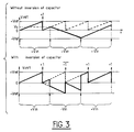
- Fig. 3 shows the effects of changing the polarity of the input signal Vin in the cases where firstly, the integrating capacitor 14 is not reversed and, secondly, where the integrating capacitor is reversed.
- the voltage Vint at the output of the amplifier 11 is at a non-zero point Vx.
- Reversing the polarity of the input signal Vin at this point in the cycle without reversing the capacitor means that, subsequently, the output of the integrator has to firstly clear off the residual charge on the integrating capacitor and then to bring the change to the capacitor to the same magnitude as at the time of the inversion but with a reverse polarity before the input signal may be integrated to the point where it rises above the reference value to the comparator 12 to control Vref of the opposite polarity to be injected. As shown in the upper figure, if the input voltage Vin is again reversed to return to a positive voltage, this point may not be reached in the available time. In contrast, where the capacitor 14 is reversed at the point of inversion of the input voltage, the integrator will commence its integration with the correct initial conditions, such that an output Q correctly reflecting the magnitude of the input voltage will result.
- CMOS constructed capacitor 13 comprising a top plate 20 and a bottom plate 21 maintained in relation to each other and to a substrate 22.
- capacitances also exist between each plate and the substrate, having the effect that the capacitor can be modelled as a single capacitor C together with two parasitic capacitances Cbot and Ctop. Due to the proximity of the lower plate 21 to the substrate 22, the bottom capacitance Cbot is considerably more significant, i.e. of the order of 10% of C, compared with 1% for Ctop.
- the integrating capacitor 14 may be arranged with its bottom plate connected to the output of the amplifier then, as the capacitor is reversed, the bottom parasitic capacitance will become connected to the input of the operational amplifier 11.
- the amplifier may be modelled as presenting an effectively infinite resistance at its inputs and a current source at its output. Accordingly, connecting Cbot to the high resistance input causes the parasitic capacitor to inject its charge into the main capacitance, causing errors in the integration. Reversing the capacitor in the opposite sense (i.e.
- Fig 5. shows an embodiment of the present invention which overcomes these problems.
- the sigma-delta circuit shown comprises a switching capacitor 30 together with associated switches ⁇ in, ⁇ ref, ⁇ ma, ⁇ ch, ⁇ dec, operating as described before, an amplifier 31 and a comparator 32 and a clocked bistable 33.
- the circuit further comprises an exclusive OR gate (EOR) 34 which includes one input connected to the timing signal ⁇ chop to demodulate the output.
- EOR exclusive OR gate
- the circuit also includes an integrating capacitor 35 together with a storage capacitor 36 arranged as shown in parallel, having twice the capacity of the integrating capacitor 35 and having associated switches ⁇ inv1 and ⁇ inv2. Referring to the timing diagram shown in Fig.
- phase pulses ⁇ 1, 2, 3, 4 are generated e.g. by a microprocessor (not shown).
- the switches ⁇ in, ⁇ ma, ⁇ ref, ⁇ ch, ⁇ dec are controlled by the microprocessor relative to these phases as in conventional circuits.
- the switch ⁇ inv1 is closed during the immediately subsequent timing sub-cycle ⁇ 4, to charge the storage capacitor 36 to the voltage Vint at the output of the amplifier, i.e. to charge the capacitor 36 to the value 2C.Vint.
- the switch ⁇ inv1 is disconnected and the switch ⁇ inv2 connected to deposit the charge 2C.Vint into the integrating capacitor 35. Immediately before this operation the capacitor 35 held the charge + C.Vint.
- the integrating capacitor 35 can be arranged with its bottom plate permanently connected to the output of the amplifier 31 in order to minimise the effects of the parasitic capacitance, the larger bottom plate capacitance being exposed only to the operation of the current source of the amplifier.
- the top plate of the capacitor 36 may be connected to the integrating capacitor, the bottom plate being permanently connected to ground, such that the most significant capacitance value is the capacitance across the main plates.
- the parasitic capacitance associated with this plate may be taken into account with the main capacitance in matching the total value of the capacitor 36 to the capacitor 35.
- the present invention is equally applicable to other in modulated integrating circuits in the input to the integrator is periodically reversed.
- the invention may be applied to one or both sigma-delta circuits used in a sigma-delta multiplication circuit, e.g. as found in the field of electricity metering.
- the output of a first sigma-delta converter controls the sign of the input of a second sigma-delta converter, such that the output of the second sigma-delta circuit is representative of the product of the input signals to each converter.
- Such multiplication circuits are described in FR 2 570 854.
- the input of the first and second converters may be the current and voltage, respectively, such that the output of the second converter represents the energy taken by a load.
- the present invention may be incorporated in one or both sigma-delta converters.
Landscapes
- Engineering & Computer Science (AREA)
- Physics & Mathematics (AREA)
- Theoretical Computer Science (AREA)
- Mathematical Physics (AREA)
- Power Engineering (AREA)
- General Physics & Mathematics (AREA)
- Software Systems (AREA)
- Computer Hardware Design (AREA)
- Compression, Expansion, Code Conversion, And Decoders (AREA)
- Amplifiers (AREA)
- Networks Using Active Elements (AREA)
- Stabilization Of Oscillater, Synchronisation, Frequency Synthesizers (AREA)
- Transforming Light Signals Into Electric Signals (AREA)
Priority Applications (7)
| Application Number | Priority Date | Filing Date | Title |
|---|---|---|---|
| ES93400130T ES2165362T3 (es) | 1993-01-20 | 1993-01-20 | Circuito integrador modulado en frecuencia. |
| DE69330744T DE69330744T2 (de) | 1993-01-20 | 1993-01-20 | Frequenzmodulierte Integratorschaltung |
| EP93400130A EP0607712B1 (de) | 1993-01-20 | 1993-01-20 | Frequenzmodulierte Integratorschaltung |
| AT93400130T ATE205620T1 (de) | 1993-01-20 | 1993-01-20 | Frequenzmodulierte integratorschaltung |
| DK93400130T DK0607712T3 (da) | 1993-01-20 | 1993-01-20 | Frekvensmoduleret integratorkredsløb |
| US08/182,877 US5459464A (en) | 1993-01-20 | 1994-01-13 | Frequency modulated integrator circuit |
| RU94001561/09A RU2144213C1 (ru) | 1993-01-20 | 1994-01-19 | Схема интегратора с частотной модуляцией |
Applications Claiming Priority (1)
| Application Number | Priority Date | Filing Date | Title |
|---|---|---|---|
| EP93400130A EP0607712B1 (de) | 1993-01-20 | 1993-01-20 | Frequenzmodulierte Integratorschaltung |
Publications (2)
| Publication Number | Publication Date |
|---|---|
| EP0607712A1 true EP0607712A1 (de) | 1994-07-27 |
| EP0607712B1 EP0607712B1 (de) | 2001-09-12 |
Family
ID=8214666
Family Applications (1)
| Application Number | Title | Priority Date | Filing Date |
|---|---|---|---|
| EP93400130A Expired - Lifetime EP0607712B1 (de) | 1993-01-20 | 1993-01-20 | Frequenzmodulierte Integratorschaltung |
Country Status (7)
| Country | Link |
|---|---|
| US (1) | US5459464A (de) |
| EP (1) | EP0607712B1 (de) |
| AT (1) | ATE205620T1 (de) |
| DE (1) | DE69330744T2 (de) |
| DK (1) | DK0607712T3 (de) |
| ES (1) | ES2165362T3 (de) |
| RU (1) | RU2144213C1 (de) |
Cited By (5)
| Publication number | Priority date | Publication date | Assignee | Title |
|---|---|---|---|---|
| EP0747849A1 (de) * | 1995-06-07 | 1996-12-11 | Landis & Gyr Technology Innovation AG | SC-Integrator mit umschaltbarer Polarität |
| EP0903863A1 (de) * | 1997-09-19 | 1999-03-24 | Motorola, Inc. | Ein-Bit-Analog-Digital-Wandler |
| US7248628B2 (en) | 2001-03-02 | 2007-07-24 | Shaeffer Derek K | Method and apparatus for a programmable filter |
| EP2275921A2 (de) | 1995-07-31 | 2011-01-19 | Canon Kabushiki Kaisha | Bildverarbeitungsgerät |
| US8102171B2 (en) | 2006-05-26 | 2012-01-24 | Rohde & Schwarz Gmbh & Co. Kg | Measuring device and measuring method for measuring the envelope power and the mean-power value |
Families Citing this family (9)
| Publication number | Priority date | Publication date | Assignee | Title |
|---|---|---|---|---|
| US6137431A (en) * | 1999-02-09 | 2000-10-24 | Massachusetts Institute Of Technology | Oversampled pipeline A/D converter with mismatch shaping |
| US6140871A (en) * | 1999-03-26 | 2000-10-31 | National Semiconductor Corporation | Switched capacitor amplifier circuit having bus precharge capability and method |
| SE514073C2 (sv) * | 1999-04-07 | 2000-12-18 | Ericsson Telefon Ab L M | Offsetkompensering i analog-digital-omvandlare |
| US7199743B2 (en) * | 2004-12-29 | 2007-04-03 | Intel Corporation | Cyclic digital to analog converter |
| KR100828271B1 (ko) * | 2005-08-05 | 2008-05-07 | 산요덴키가부시키가이샤 | 스위치 제어 회로, δ∑ 변조 회로, 및 δ∑ 변조형 ad컨버터 |
| JP4662826B2 (ja) * | 2005-08-05 | 2011-03-30 | 三洋電機株式会社 | スイッチ制御回路、δς変調回路、及びδς変調型adコンバータ |
| JP2009135595A (ja) * | 2007-11-28 | 2009-06-18 | Sony Corp | スイッチトキャパシタ回路、スイッチトキャパシタフィルタ、およびシグマデルタad変換器 |
| IT201700077220A1 (it) * | 2017-07-10 | 2019-01-10 | St Microelectronics Srl | Circuito convertitore digitale-analogico, dispositivo e procedimento corrispondenti |
| CN113094022B (zh) * | 2021-06-09 | 2021-08-20 | 广东希荻微电子股份有限公司 | 一种模拟乘法器 |
Citations (3)
| Publication number | Priority date | Publication date | Assignee | Title |
|---|---|---|---|---|
| DE2846598A1 (de) * | 1978-10-26 | 1980-04-30 | Stepper & Co | Time-division-multiplizierer insbesondere zur messung der elektrischen leistung und energie |
| EP0354060A2 (de) * | 1988-08-05 | 1990-02-07 | THE GENERAL ELECTRIC COMPANY, p.l.c. | Delta-Sigma-Modulator |
| EP0461282A1 (de) * | 1990-06-12 | 1991-12-18 | Siemens Aktiengesellschaft | Überabtastender Analog-Digital-Umsetzer mit Rauschfilterung in Switched-Capacitor-Technik |
Family Cites Families (8)
| Publication number | Priority date | Publication date | Assignee | Title |
|---|---|---|---|---|
| US3659988A (en) * | 1970-02-18 | 1972-05-02 | Phillips Petroleum Co | Bicomponent distribution plate of a spinneret assembly |
| US4009475A (en) * | 1974-12-05 | 1977-02-22 | Hybrid Systems Corporation | Delta-sigma converter and decoder |
| JPS5923261A (ja) * | 1982-07-29 | 1984-02-06 | Toshiba Corp | 電力ロ−ドサ−ベイ装置 |
| FR2570854B1 (fr) * | 1984-09-25 | 1991-01-04 | Enertec | Procede et dispositif de traitement de signal |
| CA1233890A (en) * | 1985-05-27 | 1988-03-08 | Peter Gillingham | Decimating filter |
| SU1444832A1 (ru) * | 1987-07-15 | 1988-12-15 | Организация П/Я А-3500 | Аналого-цифровой интегратор |
| SU1539800A2 (ru) * | 1988-03-11 | 1990-01-30 | Курский Политехнический Институт | Интегратор с автоматической коррекцией нулевого уровн |
| JPH04243326A (ja) * | 1991-01-18 | 1992-08-31 | Nec Corp | オーバサンプリングd−a変換器 |
-
1993
- 1993-01-20 ES ES93400130T patent/ES2165362T3/es not_active Expired - Lifetime
- 1993-01-20 AT AT93400130T patent/ATE205620T1/de not_active IP Right Cessation
- 1993-01-20 DK DK93400130T patent/DK0607712T3/da active
- 1993-01-20 EP EP93400130A patent/EP0607712B1/de not_active Expired - Lifetime
- 1993-01-20 DE DE69330744T patent/DE69330744T2/de not_active Expired - Fee Related
-
1994
- 1994-01-13 US US08/182,877 patent/US5459464A/en not_active Expired - Lifetime
- 1994-01-19 RU RU94001561/09A patent/RU2144213C1/ru not_active IP Right Cessation
Patent Citations (3)
| Publication number | Priority date | Publication date | Assignee | Title |
|---|---|---|---|---|
| DE2846598A1 (de) * | 1978-10-26 | 1980-04-30 | Stepper & Co | Time-division-multiplizierer insbesondere zur messung der elektrischen leistung und energie |
| EP0354060A2 (de) * | 1988-08-05 | 1990-02-07 | THE GENERAL ELECTRIC COMPANY, p.l.c. | Delta-Sigma-Modulator |
| EP0461282A1 (de) * | 1990-06-12 | 1991-12-18 | Siemens Aktiengesellschaft | Überabtastender Analog-Digital-Umsetzer mit Rauschfilterung in Switched-Capacitor-Technik |
Cited By (6)
| Publication number | Priority date | Publication date | Assignee | Title |
|---|---|---|---|---|
| EP0747849A1 (de) * | 1995-06-07 | 1996-12-11 | Landis & Gyr Technology Innovation AG | SC-Integrator mit umschaltbarer Polarität |
| US5689206A (en) * | 1995-06-07 | 1997-11-18 | Landis & Gyr Technology Innovation Ag | Sc-integrator with switchable polarity |
| EP2275921A2 (de) | 1995-07-31 | 2011-01-19 | Canon Kabushiki Kaisha | Bildverarbeitungsgerät |
| EP0903863A1 (de) * | 1997-09-19 | 1999-03-24 | Motorola, Inc. | Ein-Bit-Analog-Digital-Wandler |
| US7248628B2 (en) | 2001-03-02 | 2007-07-24 | Shaeffer Derek K | Method and apparatus for a programmable filter |
| US8102171B2 (en) | 2006-05-26 | 2012-01-24 | Rohde & Schwarz Gmbh & Co. Kg | Measuring device and measuring method for measuring the envelope power and the mean-power value |
Also Published As
| Publication number | Publication date |
|---|---|
| US5459464A (en) | 1995-10-17 |
| ATE205620T1 (de) | 2001-09-15 |
| DK0607712T3 (da) | 2002-01-14 |
| DE69330744T2 (de) | 2002-07-04 |
| DE69330744D1 (de) | 2001-10-18 |
| ES2165362T3 (es) | 2002-03-16 |
| RU2144213C1 (ru) | 2000-01-10 |
| EP0607712B1 (de) | 2001-09-12 |
Similar Documents
| Publication | Publication Date | Title |
|---|---|---|
| EP0607712A1 (de) | Frequenzmodulierte Integratorschaltung | |
| US4543534A (en) | Offset compensated switched capacitor circuits | |
| EP0060026B1 (de) | Verstärkerstufe mit Operationsverstärker und äquivalentem Widerstandsschaltkreis mit schaltbaren Kapazitäten | |
| US5376936A (en) | One-bit switched-capacitor D/A circuit with continuous time linearity | |
| US4555668A (en) | Gain amplifier | |
| EP0030824B1 (de) | Integrator mit geschaltetem Kondensator und seine Verwendung in einem Filter | |
| US5351050A (en) | Detent switching of summing node capacitors of a delta-sigma modulator | |
| US4808942A (en) | Continuous mode auto-zero offset amplifier or integrator | |
| US7003068B2 (en) | Device for subtracting or adding a constant amount of charge in a charge-coupled device at high operating frequencies | |
| US4496858A (en) | Frequency to voltage converter | |
| US4691125A (en) | One hundred percent duty cycle sample-and-hold circuit | |
| EP0483419A1 (de) | Ganz differenzialer Abtast- und Haltkreisaddierer | |
| US20050017793A1 (en) | Boosted sampling circuit and relative method of driving | |
| EP0055260B1 (de) | Kosinusfilter mit geschalteten kapazitäten | |
| Lee et al. | Low-sensitivity switched-capacitor ladder filters | |
| US5361037A (en) | Isolation amplifier with capacitive coupling | |
| CA1189582A (en) | Switched-capacitor modulator for quadrature modulation | |
| JPS628619A (ja) | デジタル−アナログ変換器 | |
| US5376891A (en) | Phase-sensitive rectifier arrangement with integration effect | |
| US4195273A (en) | CTD charge subtraction transversal filter | |
| US5638020A (en) | Switched capacitor differential circuits | |
| US4331944A (en) | Switched-capacitor resistor simulation circuits | |
| GB2111780A (en) | Improvements in or relating to amplifier systems | |
| WO1984004421A1 (en) | Circuit for effecting improved slew rate of operational amplifiers | |
| Hewes | A self-contained 800 stage CCD transversal filter |
Legal Events
| Date | Code | Title | Description |
|---|---|---|---|
| PUAI | Public reference made under article 153(3) epc to a published international application that has entered the european phase |
Free format text: ORIGINAL CODE: 0009012 |
|
| AK | Designated contracting states |
Kind code of ref document: A1 Designated state(s): AT BE CH DE DK ES FR GB GR IT LI NL SE |
|
| 17P | Request for examination filed |
Effective date: 19941230 |
|
| 17Q | First examination report despatched |
Effective date: 20000410 |
|
| GRAG | Despatch of communication of intention to grant |
Free format text: ORIGINAL CODE: EPIDOS AGRA |
|
| GRAG | Despatch of communication of intention to grant |
Free format text: ORIGINAL CODE: EPIDOS AGRA |
|
| GRAG | Despatch of communication of intention to grant |
Free format text: ORIGINAL CODE: EPIDOS AGRA |
|
| GRAH | Despatch of communication of intention to grant a patent |
Free format text: ORIGINAL CODE: EPIDOS IGRA |
|
| GRAH | Despatch of communication of intention to grant a patent |
Free format text: ORIGINAL CODE: EPIDOS IGRA |
|
| GRAA | (expected) grant |
Free format text: ORIGINAL CODE: 0009210 |
|
| AK | Designated contracting states |
Kind code of ref document: B1 Designated state(s): AT BE CH DE DK ES FR GB GR IT LI NL SE |
|
| REF | Corresponds to: |
Ref document number: 205620 Country of ref document: AT Date of ref document: 20010915 Kind code of ref document: T |
|
| REG | Reference to a national code |
Ref country code: CH Ref legal event code: EP |
|
| REF | Corresponds to: |
Ref document number: 69330744 Country of ref document: DE Date of ref document: 20011018 |
|
| REG | Reference to a national code |
Ref country code: GB Ref legal event code: IF02 |
|
| REG | Reference to a national code |
Ref country code: DK Ref legal event code: T3 |
|
| ET | Fr: translation filed | ||
| REG | Reference to a national code |
Ref country code: ES Ref legal event code: FG2A Ref document number: 2165362 Country of ref document: ES Kind code of ref document: T3 |
|
| REG | Reference to a national code |
Ref country code: GR Ref legal event code: EP Ref document number: 20010402420 Country of ref document: GR |
|
| PLBE | No opposition filed within time limit |
Free format text: ORIGINAL CODE: 0009261 |
|
| STAA | Information on the status of an ep patent application or granted ep patent |
Free format text: STATUS: NO OPPOSITION FILED WITHIN TIME LIMIT |
|
| 26N | No opposition filed | ||
| REG | Reference to a national code |
Ref country code: FR Ref legal event code: GC |
|
| BECH | Be: change of holder |
Owner name: *SCHLUMBERGER ELECTRICITY INC. Effective date: 20040202 |
|
| REG | Reference to a national code |
Ref country code: CH Ref legal event code: PUE Owner name: SCHLUMBERGER INDUSTRIES S.A. Free format text: SCHLUMBERGER INDUSTRIES S.A.#50, AVENUE JEAN-JAURES#92120 MONTROUGE (FR) -TRANSFER TO- SCHLUMBERGER INDUSTRIES S.A.#313-B NORTH HIGHWAY 11#WEST UNION, SC 29696 (US) Ref country code: CH Ref legal event code: NV Representative=s name: DR. LUSUARDI AG |
|
| REG | Reference to a national code |
Ref country code: CH Ref legal event code: PUE Owner name: SCHLUMBERGER INDUSTRIES S.A. Free format text: SCHLUMBERGER INDUSTRIES S.A.#50, AVENUE JEAN-JAURES#92120 MONTROUGE (FR) -TRANSFER TO- SCHLUMBERGER INDUSTRIES S.A.#313-B NORTH HIGHWAY 11#WEST UNION, SC 29696 (US) Ref country code: CH Ref legal event code: PK Free format text: RECTIFICATION. Ref country code: CH Ref legal event code: NV Representative=s name: DR. LUSUARDI AG |
|
| NLS | Nl: assignments of ep-patents |
Owner name: SCHLUMBERGER ELECTRICITY, INC. |
|
| NLT1 | Nl: modifications of names registered in virtue of documents presented to the patent office pursuant to art. 16 a, paragraph 1 |
Owner name: SCHLUMBERGER S.A. |
|
| REG | Reference to a national code |
Ref country code: FR Ref legal event code: DG |
|
| REG | Reference to a national code |
Ref country code: FR Ref legal event code: TP |
|
| REG | Reference to a national code |
Ref country code: GB Ref legal event code: 732E |
|
| PGFP | Annual fee paid to national office [announced via postgrant information from national office to epo] |
Ref country code: ES Payment date: 20090126 Year of fee payment: 17 Ref country code: DK Payment date: 20090130 Year of fee payment: 17 Ref country code: AT Payment date: 20090102 Year of fee payment: 17 |
|
| PGFP | Annual fee paid to national office [announced via postgrant information from national office to epo] |
Ref country code: NL Payment date: 20090124 Year of fee payment: 17 Ref country code: DE Payment date: 20090302 Year of fee payment: 17 |
|
| PGFP | Annual fee paid to national office [announced via postgrant information from national office to epo] |
Ref country code: GR Payment date: 20090129 Year of fee payment: 17 Ref country code: GB Payment date: 20090129 Year of fee payment: 17 Ref country code: CH Payment date: 20090126 Year of fee payment: 17 |
|
| PGFP | Annual fee paid to national office [announced via postgrant information from national office to epo] |
Ref country code: BE Payment date: 20090219 Year of fee payment: 17 |
|
| PGFP | Annual fee paid to national office [announced via postgrant information from national office to epo] |
Ref country code: SE Payment date: 20090128 Year of fee payment: 17 Ref country code: IT Payment date: 20090129 Year of fee payment: 17 |
|
| PGFP | Annual fee paid to national office [announced via postgrant information from national office to epo] |
Ref country code: FR Payment date: 20090119 Year of fee payment: 17 |
|
| BERE | Be: lapsed |
Owner name: *SCHLUMBERGER ELECTRICITY INC. Effective date: 20100131 |
|
| REG | Reference to a national code |
Ref country code: NL Ref legal event code: V1 Effective date: 20100801 |
|
| REG | Reference to a national code |
Ref country code: CH Ref legal event code: PL |
|
| REG | Reference to a national code |
Ref country code: DK Ref legal event code: EBP |
|
| GBPC | Gb: european patent ceased through non-payment of renewal fee |
Effective date: 20100120 |
|
| EUG | Se: european patent has lapsed | ||
| REG | Reference to a national code |
Ref country code: FR Ref legal event code: ST Effective date: 20100930 |
|
| PG25 | Lapsed in a contracting state [announced via postgrant information from national office to epo] |
Ref country code: NL Free format text: LAPSE BECAUSE OF NON-PAYMENT OF DUE FEES Effective date: 20100801 Ref country code: LI Free format text: LAPSE BECAUSE OF NON-PAYMENT OF DUE FEES Effective date: 20100131 Ref country code: FR Free format text: LAPSE BECAUSE OF NON-PAYMENT OF DUE FEES Effective date: 20100201 Ref country code: CH Free format text: LAPSE BECAUSE OF NON-PAYMENT OF DUE FEES Effective date: 20100131 |
|
| PG25 | Lapsed in a contracting state [announced via postgrant information from national office to epo] |
Ref country code: DE Free format text: LAPSE BECAUSE OF NON-PAYMENT OF DUE FEES Effective date: 20100803 Ref country code: AT Free format text: LAPSE BECAUSE OF NON-PAYMENT OF DUE FEES Effective date: 20100120 |
|
| PG25 | Lapsed in a contracting state [announced via postgrant information from national office to epo] |
Ref country code: GB Free format text: LAPSE BECAUSE OF NON-PAYMENT OF DUE FEES Effective date: 20100120 |
|
| PG25 | Lapsed in a contracting state [announced via postgrant information from national office to epo] |
Ref country code: DK Free format text: LAPSE BECAUSE OF NON-PAYMENT OF DUE FEES Effective date: 20100131 |
|
| PG25 | Lapsed in a contracting state [announced via postgrant information from national office to epo] |
Ref country code: BE Free format text: LAPSE BECAUSE OF NON-PAYMENT OF DUE FEES Effective date: 20100131 |
|
| PG25 | Lapsed in a contracting state [announced via postgrant information from national office to epo] |
Ref country code: IT Free format text: LAPSE BECAUSE OF NON-PAYMENT OF DUE FEES Effective date: 20100120 |
|
| REG | Reference to a national code |
Ref country code: ES Ref legal event code: FD2A Effective date: 20111118 |
|
| PG25 | Lapsed in a contracting state [announced via postgrant information from national office to epo] |
Ref country code: ES Free format text: LAPSE BECAUSE OF NON-PAYMENT OF DUE FEES Effective date: 20100121 |
|
| PG25 | Lapsed in a contracting state [announced via postgrant information from national office to epo] |
Ref country code: SE Free format text: LAPSE BECAUSE OF NON-PAYMENT OF DUE FEES Effective date: 20100121 |