EP0607944B1 - Automatische Verstärkungsregelung für Burstsignale - Google Patents
Automatische Verstärkungsregelung für Burstsignale Download PDFInfo
- Publication number
- EP0607944B1 EP0607944B1 EP94100722A EP94100722A EP0607944B1 EP 0607944 B1 EP0607944 B1 EP 0607944B1 EP 94100722 A EP94100722 A EP 94100722A EP 94100722 A EP94100722 A EP 94100722A EP 0607944 B1 EP0607944 B1 EP 0607944B1
- Authority
- EP
- European Patent Office
- Prior art keywords
- signal
- loop
- subtractor
- output signal
- multiplier
- Prior art date
- Legal status (The legal status is an assumption and is not a legal conclusion. Google has not performed a legal analysis and makes no representation as to the accuracy of the status listed.)
- Expired - Lifetime
Links
Images

Classifications
-
- H—ELECTRICITY
- H03—ELECTRONIC CIRCUITRY
- H03G—CONTROL OF AMPLIFICATION
- H03G3/00—Gain control in amplifiers or frequency changers
- H03G3/20—Automatic control
- H03G3/30—Automatic control in amplifiers having semiconductor devices
- H03G3/3036—Automatic control in amplifiers having semiconductor devices in high-frequency amplifiers or in frequency-changers
- H03G3/3042—Automatic control in amplifiers having semiconductor devices in high-frequency amplifiers or in frequency-changers in modulators, frequency-changers, transmitters or power amplifiers
- H03G3/3047—Automatic control in amplifiers having semiconductor devices in high-frequency amplifiers or in frequency-changers in modulators, frequency-changers, transmitters or power amplifiers for intermittent signals, e.g. burst signals
Definitions
- the present invention relates to an AGC circuit for burst signals in a burst signal demodulator, such as for voice activation, slotted aloha, TDMA, etc.
- a voice activation method which operates according to a talker's intermittent voice generation characteristic such as to transmit a signal when there is a voice and transmit no signal when there is no voice is useful for effective utilisation of satellite power and is extensively employed.
- a signal modulation wave is an intermittently transmitted signal, i.e., a burst signal. Therefore, a burst demodulator is required on the receive side.
- a received level on the receive side is varied with variations of the communication channel transmission loss (each base station).
- the loop gain of the demodulator's carrier recovery circuit or the clock recovery circuit is varied, and a stable demodulation operation can not longer be obtained. Therefore, an AGC operation for maintaining a constant received signal level is required.
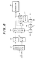
- Fig. 6 shows a block diagram of a conventional AGC circuit.
- a quasi-synchronization demodulator 21 receives an intermittently transmitted burst modulated signal (IF input signal) for quasi-synchronization demodulation with orthogonal carrier wave signals which are substantially equal in frequency to the carrier wave frequency to obtain two quadrature channels of analog type.
- A/D converters 22 and 23 convert the two output signals from the quasi-synchronization demodulator 21 into respective digital data series consisting of a plurality of bits.
- the digital data series obtained by the A/D converters 22 and 23 are applied to a multiplier 24.
- the output of the multiplier 24 is supplied to a demodulator 31 using a DSP (Digital Signal Processor), and also to square circuits 25 and 26.
- DSP Digital Signal Processor
- the received signal level is obtained by squaring the respective outputs of the multiplier 24.
- the received signal levels of the data series obtained by the squaring circuits 25 and 26 are added in an adder 27 to obtain the received signal power of the outputs of the multiplier 24.
- a subtractor 28 subtracts an output signal level of the adder 27 from a reference value R1 to be set by the AGC loop.
- the difference value of the output of the subtractor 28 is multiplied by a multiplier 29 with a loop gain constant k which determines the AGC loop gain, and the multiplied result is applied to an integrator 30.
- the integrator 30 integrates the output of the multiplier 29 and drives the multiplier 24.
- the AGC loop is thus established in order to minimize the output value of the subtractor 28.
- the AGC response time thereof is determined by the loop gain constant k; the response time becomes shorter with a greater gain constant k and becomes longer with a smaller loop gain constant k.
- JP-A-59-135915 discloses an AGC circuit for receiving a transmitted signal, and demodulating said signal and a selector for selecting one of three different loop constants based upon the output signal of a decision unit.
- An object of the invention is therefore to provide an AGC circuit for burst signals capable of a high quality demodulation.
- Another object of the invention is to provide an AGC circuit for burst signals, in which the AGC loop has a high speed response characteristic when a high speed synchronization is necessary in the initial state, while the AGC loop band becomes minimum and the loop noise vanishes after the high speed response state.
- Fig. 1 is a block diagram showing a first embodiment.
- parts like those in the AGC circuit shown in Fig. 6 are designated by like reference numerals.
- an area decision unit 11 and a selector 12 are added to the system shown in Fig. 6.
- the area decision unit 11 converts the output signal of the subtractor 28 into a three-state signal by comparing the output signal level with reference values R2 and R3.
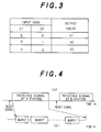
- the output signal IV from the subtractor 28 is decided with respect to the reference values R2 and R3 as in Fig. 2.
- Shown at C1 and C2 are two-bit data of the output signal of the area decision unit 11.
- the reference value R2 is set to be greater than the reference value R3.
- the area decision unit 11 sets C1 to "0" and C2 to “0” if the output signal IV of the subtractor 28 is greater than the reference value R2, sets C1 to “1” and C2 to “0” if the output signal IV of the subtractor 28 is less than the reference value R3, and sets C1 to "0” and C2 to "1” if the output signal IV of the subtractor 28 has an intermediate value between the reference values R2 and R3.
- the selector 12 receives the output signal of the subtractor 28 and selects either one of loop constants K1 to K3 as shown in Fig. 3 in accordance with the input codes C1 and C2.
- the loop constants K1 to K3 are set as K1 >> K2 ⁇ K3.
- the selector 12 selects the loop constant K1 if C1 and C2 are both "0", selects the loop constant K2 if C1 and C2 are respectively "0" and "1” and selects the loop constant K3 if C1 and C2 are respectively "1" and "0".
- the selector 12 selects the loop constant K1 if the output signal of the subtractor 28 is greater than the reference value R2, selects the loop constant K3 if the output signal of the subtractor 28 is less than the reference value R3, and selects the loop constant K2 if the output signal of the subtractor 28 has an intermediate value between the reference values R2 and R3.
- the signal selected by the selector 12 is supplied to the multiplier 29 for determining the gain of the AGC loop.
- the output value of the adder 27 is less than the reference value R1, and the subtractor 28 generates a negative output.
- the selector 12 executes the selection operation based upon a table as shown in Fig. 3, and selects a loop constant K3.
- This loop constant K3 is input to the multiplier 29. If K1 to K3 are related as K1 >> K2 ⁇ K3 as noted above, the AGC loop band is held at a minimum.
- the output signal of the multiplier 29 is negative (that is a small input signal) even though K3 has a small value.
- the input to the integrator 30 thus controls the multiplier 24 to provide for the maximum gain so as to increase the input signal.
- Figs. 4(a) and 4(b) show an operation in case when the demodulator first communicates with a station A and then communicates with a station B. In this case, the reset signal is supplied before the start of the communication. When making communication with station B after the communication with station A has been ended, a reset signal is input prior to the start of the communication.
- Fig. 4(b) shows a case when the burst signal is transmitted on the basis of generation of the talker's speech in station A.
- the output of the subtractor 28 When the received signal vanishes, the output of the subtractor 28 is held at a negative value. In many cases, at this moment the output of the subtractor 28 becomes less than the reference value R3, and the selector 12 selectively provides the loop constant K3 to the multiplier 29. Since the loop constant K3 is sufficiently small, only a very small value is supplied to the integrator 30 subsequent to the multiplier 29. Thus, the output of the integrator 30 is held substantially at a constant value for a long time (compared with the interval of the voice activation signal burst). The gain of the multiplier 24 is thus held substantially at the same value as when there is a burst signal.
- the gain of the multiplier 24 is held to be substantially ideal, and the time required for the next pull-in is extremely reduced. If the input signal is great compared with the previous burst, the loop constant K1 is selected to provide for high speed response of the AGC loop as noted above. If the input signal is less compared with the previous burst, however, time-consuming response is liable. In the voice activation or like system, the transmitting station is the same, and the level difference is small and has substantially no influence on the subsequent demodulator.
- the reference value R3 is set in the lower range of the demodulator.
- the loop constant K2 is supplied to the multiplier 29 according to table shown in Fig. 2.
- the level deviation from the desired level is very small compared with that at the time of the initial reception.
- the loop band need not be considerably great(that is, there is no need to follow high speed).
- the loop constant K2 is set to a value which is considerably smaller than the loop constant K1 and greater than the loop constant K3.
- the demodulator is immediately set to a level permitting stable operation.
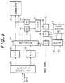
- Fig. 5 shows a block diagram showing a second embodiment of the present invention.
- parts like those shown in Fig. 6 are designated by like reference numerals.
- the embodiment of Fig. 5 is formed by adding a selector 12 and a polarity detection unit 13 to the structure shown in Fig. 6.
- the polarity detection unit 13 receives the output signal of the subtractor 28 which detects the difference between a reference value R1 and the received level, and detects the polarity of the input.
- the detected polarity signal is applied to the selector 12.
- the selector 12 selects the loop constant K1 if the polarity of the polarity detection unit 13 is positive and selects the loop constant K2 if the polarity of the polarity detection unit 13 is negative.
- K1 >> K2.
- the selected loop constant K1 or K2 is input to the multiplier 29, which determines the AGC loop gain.
- the second embodiment Before receiving the signal, the received power is low because at this time at most noise components present in the channel are received. Thus, the output value of the adder 27 is less than the reference value R1, and the polarity detection unit 13 generates a negative output. The polarity detection unit 13 thus generates a negative signal, and the selector 12 generates the loop constant K2 as its output. The subtractor 28 provides the loop constant K2 as its output. Thus, if the loop constant K2 meets K2 ⁇ K1 and can hold the loop band to be narrow, the AGO loop waits with a low speed response characteristic. However, since no signal has been received, the multiplier 24 normally has a maximum gain.
- the loop constant K1 is set as a constant in the multiplier 29 by the polarity detection unit 13 and the selector 12.
- the loop constant K1 is sufficiently greater than the loop constant K2, that is K1 >> K2, and the loop band is widened.
- the AGC band is widened and the high speed response to the input signal is realized.
- the signal power that is input to the demodulator 31 from the multiplier 24 rapidly becomes coincident with the reference value R1, and thus the output signal of the subtractor 28 becomes zero.
- the selector 12 is controlled to select the loop constant K2. Since at this time the loop constant K2 is sufficiently small compared with K1, the noise in the AGC loop is sufficiently small, and the signal deterioration is held minimum. Thus, when the high speed synchronization is required, the AGC loop band is increased, and after a pull-in the AGC loop band is reduced to minimize the signal deterioration.
- the output of the subtractor 28 is held negative, and thus the loop constant K2 remains set in the subtractor 28. Since the loop constant K2 is sufficiently small, the integrator 30 subsequent to the multiplier 29 is supplied with only a very small value. The value of the integrator 30 is thus held substantially constant for a long time. Thus, the gain of the multiplier 24 is held substantially at the same value as when there is a burst signal.
- the gain of the multiplier 24 is held to be substantially ideal, and thus the time required for the next pull-in is extremely reduced.
- the response takes time.
- the transmitter earth station is the same.
- the level difference is small and has no effect on the subsequent demodulator.
- the level difference between adjacent bursts is at most about 3 dB and has substantially no effect on the demodulator.
- the AG0 loop when the high speed synchronization is necessary in the initial stage, the AG0 loop has the high speed response characteristic, and after that the high speed response the AGC loop band becomes minimum, and also the influence of the loop noise vanishes.
- the AGC loop band is set to be minimum, thus setting the gain of the gain control multiplier with respect to the previous burst level.
- the intermediate loop band is selected to absorb the inter-burst deviation.
Landscapes
- Control Of Amplification And Gain Control (AREA)
- Circuits Of Receivers In General (AREA)
Claims (7)
- AGC-Schaltung für Burstsignale mit:wobei die Schleifenkonstanten K1, K2 und K3 die Beziehung K1 » K2 ≥ K3 haben, der erste Referenzwert so eingestellt ist, daß er größer als der zweite Referenzwert ist, und der Selektor (12) die Schleifenkonstante K1 auswählt, wenn das Ausgangssignal des Subtrahierers größer als der erste Referenzwert ist, die Schleifenkonstante K3 auswählt, wenn das Ausgangssignal des Subtrahierers (28) kleiner als der zweite Referenzwert ist, und die Schleifenkonstante K2 auswählt, wenn das Ausgangssignal des Subtrahierers einen Zwischenwert zwischen dem ersten und zweiten Referenzwert hat.a) einem Quasisynchronisationsdemodulator (21) zum Empfangen eines intermittierend gesendeten Burstmodulationssignals und Demodulieren des Burstmodulationssignals in ein Basisbandsignal,b) einem Selektor (12) zum Auswählen einer von drei vorbestimmten unterschiedlichen Schleifenkonstanten K1, K2 und K3 auf der Grundlage des Ausgangssignals einer Bereichsentscheidungseinheit, gekennzeichnet durch:c) zwei Analog-Digital-Wandler (22, 23) zum Umwandeln des Ausgangssignals des Quasisynchronisationsdemodulators in ein digitales Signal,d) einen ersten Multiplizierer (24) zum Empfangen der Ausgangssignale der Analog-Digital-Wandler und eines Integrators (30) und Durchführen einer Multiplikationsoperation,e) zwei Quadrierschaltungen (25, 26) zum Quadrieren des Ausgangssignals des ersten Multiplizierers,f) eine Addiererschaltung (27) zum Addieren der Ausgangssignale der Quadrierschaltungen,g) einen digitalen Subtrahierer (28) zum Subtrahieren eines vorbestimmten Referenzsignals (R1) von der Ausgabe der Addiererschaltung,h) eine Bereichsentscheidungseinheit (11) zum Entscheiden über drei unterschiedliche Bereiche, die durch Vergleichen eines ersten und zweiten vorbestimmten Referenzwerts mit dem Pegel des Subtrahiererausgangssignals festgelegt sind,i) einen zweiten Multiplizierer (29) zum Multiplizieren der Ausgangssignale des Selektors (12) und des Subtrahierers (28), wobei der Integrator (30) zum Integrieren des Ausgangssignals des zweiten Multiplizierers (29) zum Ansteuern des ersten Multiplizierers (24) damit vorgesehen ist, und
- AGC-Schaltung nach Anspruch 1, wobei der Integrator (30) bei Kommunikationsbeginn zurückgesetzt wird.
- AGC-Schaltung nach Anspruch 1 oder 2, wobei eine digitale Polaritätsdetektionseinheit (13) als Entscheidungseinheit zum Detektieren einer Polarität des Ausgangssignals des Subtrahierers (28) verwendet wird und der Selektor (12) die Schleifenkonstante K1 auswählt, wenn durch die Polaritätsdetektionseinheit detektiert wird, daß das Ausgangssignal des Subtrahierers positiv ist, und die Schleifenkonstante K2 (K1 » K2) auswählt, wenn das Ausgangssignal des Subtrahierers negativ ist.
- AGC-Verfahren für Burstsignale mit den folgenden Schritten:einem ersten Schritt zum Quasidemodulieren eines intermittierend gesendeten Burstmodulationswellensignals in ein Basisbandsignal;einem zweiten Schritt zum Multiplizieren des Basisbandsignals mit einem variablen Verstärkungskoeffizienten;einem dritten Schritt zum Erhalten eines Empfangssignalpegels durch Verwendung des multiplizierten Signals;einem vierten Schritt zum Entscheiden über einen Bereich, in dem ein Differenzsignal des Empfangssignalpegels von einem Referenzpegel liegt, unter mehreren Pegelbereichen;einem fünften Schritt zum Bestimmen einer Schleifenkonstante in Übereinstimmung mit dem Entscheidungsbereich;einem sechsten Schritt zum Multiplizieren des Differenzsignals mit der bestimmten Schleifenkonstante;einem siebenten Schritt zum Integrieren des multiplizierten Differenzsignals mit der Schleifenkonstante; undeinem achten Schritt zum Ändern der variablen Verstärkungskoeffizienten in dem zweiten Schritt.
- Verfahren nach Anspruch 4, wobei der integrierte Wert in dem siebenten Schritt bei Kommunikationsbeginn zurückgesetzt wird.
- Verfahren nach Anspruch 4 oder 5, wobei die mehreren Pegelbereiche durch einen ersten Referenzwert und einen zweiten Referenzwert festgelegt sind, der größer als der erste Referenzwert ist, und die Schleifenkonstanten K1 bis K3 sind, die in der Beziehung K1 » K2 ≥ K3 stehen.
- Verfahren nach Anspruch 4, 5 oder 6, wobei die mehreren Pegelbereiche durch einen Referenzwert festgelegt und die Schleifenkonstanten K1 und K2 sind, die in der Beziehung K1 » K2 stehen.
Applications Claiming Priority (4)
| Application Number | Priority Date | Filing Date | Title |
|---|---|---|---|
| JP7945/93 | 1993-01-20 | ||
| JP7850/93 | 1993-01-20 | ||
| JP5007850A JP2500577B2 (ja) | 1993-01-20 | 1993-01-20 | バ―スト信号用agc回路 |
| JP5007945A JP2500578B2 (ja) | 1993-01-20 | 1993-01-20 | バ―スト信号用agc回路 |
Publications (2)
| Publication Number | Publication Date |
|---|---|
| EP0607944A1 EP0607944A1 (de) | 1994-07-27 |
| EP0607944B1 true EP0607944B1 (de) | 1998-09-16 |
Family
ID=26342236
Family Applications (1)
| Application Number | Title | Priority Date | Filing Date |
|---|---|---|---|
| EP94100722A Expired - Lifetime EP0607944B1 (de) | 1993-01-20 | 1994-01-19 | Automatische Verstärkungsregelung für Burstsignale |
Country Status (5)
| Country | Link |
|---|---|
| US (1) | US5452332A (de) |
| EP (1) | EP0607944B1 (de) |
| CN (1) | CN1052591C (de) |
| AU (1) | AU673390B2 (de) |
| DE (1) | DE69413264T2 (de) |
Families Citing this family (19)
| Publication number | Priority date | Publication date | Assignee | Title |
|---|---|---|---|---|
| DE69428883T2 (de) * | 1993-08-11 | 2002-04-11 | Ntt Docomo, Inc. | Gerät und verfahren zur automatischen verstärkungsregelung für einen spreizspektrum empfänger |
| US6026131A (en) * | 1995-12-27 | 2000-02-15 | Laurent; Souef | Automatic gain control systems |
| US5784410A (en) * | 1996-06-03 | 1998-07-21 | Matsushita Electric Industrial Co., Ltd. | Reception automatic gain control system and method |
| GB2314705B (en) * | 1996-06-25 | 2000-06-28 | Nec Technologies | Frequency hopping communications receivers |
| AU744861B2 (en) * | 1997-12-24 | 2002-03-07 | Nec Corporation | Frequency hopping communications receivers |
| CA2232754A1 (en) * | 1996-09-05 | 1998-03-12 | Mitsubishi Denki Kabushiki Kaisha | Gain control method and receiver |
| CA2273239C (en) * | 1996-12-13 | 2003-06-10 | John Gerard Beerends | Device and method for signal quality determination |
| FI106670B (fi) * | 1997-12-08 | 2001-03-15 | Nokia Networks Oy | Vastaanottomenetelmä ja vastaanotin |
| US6289044B1 (en) * | 1998-05-12 | 2001-09-11 | Nortel Networks Limited | Automatic gain control circuit for a modem receiver |
| BR9909264A (pt) * | 1998-09-28 | 2002-01-02 | Matsushita Eletric Industrtial | Receptor vsb |
| JP2001284996A (ja) * | 2000-03-31 | 2001-10-12 | Matsushita Electric Ind Co Ltd | ゲイン制御装置 |
| JP3479839B2 (ja) | 2000-10-27 | 2003-12-15 | 日本電気株式会社 | 受信agc回路 |
| JP3599001B2 (ja) * | 2001-06-25 | 2004-12-08 | ソニー株式会社 | 自動利得制御回路およびその方法、並びにそれらを用いた復調装置 |
| US20110119062A1 (en) * | 2005-09-29 | 2011-05-19 | Dohan Jewel L | Voice-recognition/voice-activated vehicle signal system |
| JP4997833B2 (ja) * | 2006-05-30 | 2012-08-08 | 沖電気工業株式会社 | 自動利得制御装置 |
| EP2053739A4 (de) * | 2006-12-15 | 2010-10-06 | Panasonic Corp | Digitales agc gerät |
| CN101814902B (zh) * | 2009-02-24 | 2013-09-04 | 瑞昱半导体股份有限公司 | 增益控制电路和增益控制方法 |
| US8760538B2 (en) | 2011-01-21 | 2014-06-24 | Exelis, Inc. | Adaptive gain control image processing system and method |
| CN102665267B (zh) | 2012-04-12 | 2015-12-16 | 华为技术有限公司 | 一种功率调整方法及装置 |
Family Cites Families (7)
| Publication number | Priority date | Publication date | Assignee | Title |
|---|---|---|---|---|
| JPS59135915A (ja) * | 1983-01-25 | 1984-08-04 | Matsushita Electric Ind Co Ltd | 入力レベル検出回路 |
| US4703282A (en) * | 1985-06-29 | 1987-10-27 | Nec Corporation | Digital demodulation system |
| US5040194A (en) * | 1986-07-15 | 1991-08-13 | Hayes Microcomputer Products, Inc. | Method and apparatus for providing for automatic gain control of incoming signals in a modem |
| JPS6382010A (ja) * | 1986-09-25 | 1988-04-12 | Nec Corp | 自動利得制御装置 |
| IT1230401B (it) * | 1989-06-15 | 1991-10-21 | Italtel Spa | Ricevitore a conversione diretta per segnali numerici e metodo per la demodulazione di tali segnali. |
| BE1004402A6 (fr) * | 1989-08-30 | 1992-11-17 | Internat Ind Engineering S A | Dispositif de coulee obturable pour un conteneur siderurgique ou metallurgique. |
| JPH0812979B2 (ja) * | 1989-11-21 | 1996-02-07 | 日本電気株式会社 | 自動利得制御装置 |
-
1994
- 1994-01-18 AU AU53865/94A patent/AU673390B2/en not_active Ceased
- 1994-01-19 DE DE69413264T patent/DE69413264T2/de not_active Expired - Fee Related
- 1994-01-19 US US08/184,245 patent/US5452332A/en not_active Expired - Lifetime
- 1994-01-19 EP EP94100722A patent/EP0607944B1/de not_active Expired - Lifetime
- 1994-01-20 CN CN94102659A patent/CN1052591C/zh not_active Expired - Fee Related
Also Published As
| Publication number | Publication date |
|---|---|
| AU5386594A (en) | 1994-07-28 |
| AU673390B2 (en) | 1996-11-07 |
| CN1052591C (zh) | 2000-05-17 |
| US5452332A (en) | 1995-09-19 |
| CN1099207A (zh) | 1995-02-22 |
| DE69413264D1 (de) | 1998-10-22 |
| EP0607944A1 (de) | 1994-07-27 |
| DE69413264T2 (de) | 1999-03-04 |
Similar Documents
| Publication | Publication Date | Title |
|---|---|---|
| EP0607944B1 (de) | Automatische Verstärkungsregelung für Burstsignale | |
| US4587662A (en) | TDMA spread-spectrum receiver with coherent detection | |
| US6377620B1 (en) | Balancing amplitude and phase | |
| CA2207350C (en) | Gain controller | |
| US5946607A (en) | Method of apparatus for automatic gain control, and digital receiver using same | |
| GB2326782A (en) | Selection of amplifiers in a transmitter in dependence on the data to be transmitted or a pilot signal and a required power | |
| US5533064A (en) | Digital radio receiver having limiter amplifiers and logarithmic detector | |
| US5612972A (en) | Spectrum spread signal reception with differential demodulation of spectrum spread demodulated components at each synchronous point and at a point always one symbol period later | |
| US7149263B2 (en) | AGC method and circuit for digital radio receiver | |
| US6121828A (en) | Demodulator | |
| US7386285B2 (en) | Automatic gain control adaptive for plural modulation schemes | |
| US7894785B2 (en) | Amplifier assembly, receiver comprising said assembly and method for operating a programmable amplifier | |
| WO2001028106A1 (en) | Receiver, transceiver, radio unit and method for telecommunication | |
| JPH04259125A (ja) | 自動等化器 | |
| US5638400A (en) | Receiver | |
| US6295445B1 (en) | Automatic gain controlling method, automatic gain controlling apparatus, and communication receiving apparatus | |
| US5668829A (en) | Spread spectrum communication apparatus | |
| US7443934B2 (en) | Method and apparatus for detecting signals, and transmitting apparatus and receiving apparatus using the same | |
| WO1999023777A1 (fr) | Emetteur et recepteur pour systeme de communication a plusieurs vitesses a spectre disperse direct par multiplexage du temps de propagation, et systeme precite | |
| US5625647A (en) | Transmitter having automatic level control function | |
| JPH06216955A (ja) | バースト信号用agc回路 | |
| US4559635A (en) | Auto-adaptive amplitude-equalizing arrangement for digital radio links | |
| JPH0794981A (ja) | 自動利得制御回路 | |
| JPH0918533A (ja) | バースト信号用agc回路 | |
| JPH09294146A (ja) | 自動利得制御回路 |
Legal Events
| Date | Code | Title | Description |
|---|---|---|---|
| PUAI | Public reference made under article 153(3) epc to a published international application that has entered the european phase |
Free format text: ORIGINAL CODE: 0009012 |
|
| 17P | Request for examination filed |
Effective date: 19940429 |
|
| AK | Designated contracting states |
Kind code of ref document: A1 Designated state(s): DE FR GB IT NL SE |
|
| 17Q | First examination report despatched |
Effective date: 19960813 |
|
| GRAG | Despatch of communication of intention to grant |
Free format text: ORIGINAL CODE: EPIDOS AGRA |
|
| GRAG | Despatch of communication of intention to grant |
Free format text: ORIGINAL CODE: EPIDOS AGRA |
|
| GRAG | Despatch of communication of intention to grant |
Free format text: ORIGINAL CODE: EPIDOS AGRA |
|
| GRAH | Despatch of communication of intention to grant a patent |
Free format text: ORIGINAL CODE: EPIDOS IGRA |
|
| GRAH | Despatch of communication of intention to grant a patent |
Free format text: ORIGINAL CODE: EPIDOS IGRA |
|
| GRAA | (expected) grant |
Free format text: ORIGINAL CODE: 0009210 |
|
| AK | Designated contracting states |
Kind code of ref document: B1 Designated state(s): DE FR GB IT NL SE |
|
| REF | Corresponds to: |
Ref document number: 69413264 Country of ref document: DE Date of ref document: 19981022 |
|
| ET | Fr: translation filed | ||
| PLBE | No opposition filed within time limit |
Free format text: ORIGINAL CODE: 0009261 |
|
| STAA | Information on the status of an ep patent application or granted ep patent |
Free format text: STATUS: NO OPPOSITION FILED WITHIN TIME LIMIT |
|
| 26N | No opposition filed | ||
| REG | Reference to a national code |
Ref country code: GB Ref legal event code: IF02 |
|
| PGFP | Annual fee paid to national office [announced via postgrant information from national office to epo] |
Ref country code: NL Payment date: 20090115 Year of fee payment: 16 Ref country code: DE Payment date: 20090115 Year of fee payment: 16 |
|
| PGFP | Annual fee paid to national office [announced via postgrant information from national office to epo] |
Ref country code: GB Payment date: 20090114 Year of fee payment: 16 |
|
| PGFP | Annual fee paid to national office [announced via postgrant information from national office to epo] |
Ref country code: SE Payment date: 20090108 Year of fee payment: 16 Ref country code: IT Payment date: 20090127 Year of fee payment: 16 |
|
| PGFP | Annual fee paid to national office [announced via postgrant information from national office to epo] |
Ref country code: FR Payment date: 20090113 Year of fee payment: 16 |
|
| REG | Reference to a national code |
Ref country code: NL Ref legal event code: V1 Effective date: 20100801 |
|
| GBPC | Gb: european patent ceased through non-payment of renewal fee |
Effective date: 20100119 |
|
| EUG | Se: european patent has lapsed | ||
| REG | Reference to a national code |
Ref country code: FR Ref legal event code: ST Effective date: 20100930 |
|
| PG25 | Lapsed in a contracting state [announced via postgrant information from national office to epo] |
Ref country code: NL Free format text: LAPSE BECAUSE OF NON-PAYMENT OF DUE FEES Effective date: 20100801 Ref country code: FR Free format text: LAPSE BECAUSE OF NON-PAYMENT OF DUE FEES Effective date: 20100201 |
|
| PG25 | Lapsed in a contracting state [announced via postgrant information from national office to epo] |
Ref country code: DE Free format text: LAPSE BECAUSE OF NON-PAYMENT OF DUE FEES Effective date: 20100803 |
|
| PG25 | Lapsed in a contracting state [announced via postgrant information from national office to epo] |
Ref country code: GB Free format text: LAPSE BECAUSE OF NON-PAYMENT OF DUE FEES Effective date: 20100119 |
|
| PG25 | Lapsed in a contracting state [announced via postgrant information from national office to epo] |
Ref country code: IT Free format text: LAPSE BECAUSE OF NON-PAYMENT OF DUE FEES Effective date: 20100119 |
|
| PG25 | Lapsed in a contracting state [announced via postgrant information from national office to epo] |
Ref country code: SE Free format text: LAPSE BECAUSE OF NON-PAYMENT OF DUE FEES Effective date: 20100120 |