EP0608077B1 - Réseau de résistances comprenant des circuits téléphoniques - Google Patents
Réseau de résistances comprenant des circuits téléphoniques Download PDFInfo
- Publication number
- EP0608077B1 EP0608077B1 EP94300262A EP94300262A EP0608077B1 EP 0608077 B1 EP0608077 B1 EP 0608077B1 EP 94300262 A EP94300262 A EP 94300262A EP 94300262 A EP94300262 A EP 94300262A EP 0608077 B1 EP0608077 B1 EP 0608077B1
- Authority
- EP
- European Patent Office
- Prior art keywords
- substrate
- traces
- resistor
- films
- resistive
- Prior art date
- Legal status (The legal status is an assumption and is not a legal conclusion. Google has not performed a legal analysis and makes no representation as to the accuracy of the status listed.)
- Expired - Lifetime
Links
Images
Classifications
-
- H—ELECTRICITY
- H01—ELECTRIC ELEMENTS
- H01C—RESISTORS
- H01C13/00—Resistors not provided for elsewhere
- H01C13/02—Structural combinations of resistors
-
- H—ELECTRICITY
- H04—ELECTRIC COMMUNICATION TECHNIQUE
- H04M—TELEPHONIC COMMUNICATION
- H04M19/00—Current supply arrangements for telephone systems
- H04M19/001—Current supply source at the exchanger providing current to substations
-
- H—ELECTRICITY
- H01—ELECTRIC ELEMENTS
- H01H—ELECTRIC SWITCHES; RELAYS; SELECTORS; EMERGENCY PROTECTIVE DEVICES
- H01H85/00—Protective devices in which the current flows through a part of fusible material and this current is interrupted by displacement of the fusible material when this current becomes excessive
- H01H85/02—Details
- H01H85/04—Fuses, i.e. expendable parts of the protective device, e.g. cartridges
- H01H85/041—Fuses, i.e. expendable parts of the protective device, e.g. cartridges characterised by the type
- H01H85/048—Fuse resistors
- H01H2085/0483—Fuse resistors with temperature dependent resistor, e.g. thermistor
-
- H—ELECTRICITY
- H01—ELECTRIC ELEMENTS
- H01H—ELECTRIC SWITCHES; RELAYS; SELECTORS; EMERGENCY PROTECTIVE DEVICES
- H01H85/00—Protective devices in which the current flows through a part of fusible material and this current is interrupted by displacement of the fusible material when this current becomes excessive
- H01H85/0039—Means for influencing the rupture process of the fusible element
- H01H85/0073—Expansion or rupture of the insulating support for the fusible element
-
- H—ELECTRICITY
- H01—ELECTRIC ELEMENTS
- H01H—ELECTRIC SWITCHES; RELAYS; SELECTORS; EMERGENCY PROTECTIVE DEVICES
- H01H85/00—Protective devices in which the current flows through a part of fusible material and this current is interrupted by displacement of the fusible material when this current becomes excessive
- H01H85/02—Details
- H01H85/04—Fuses, i.e. expendable parts of the protective device, e.g. cartridges
- H01H85/041—Fuses, i.e. expendable parts of the protective device, e.g. cartridges characterised by the type
- H01H85/046—Fuses formed as printed circuits
-
- H—ELECTRICITY
- H01—ELECTRIC ELEMENTS
- H01H—ELECTRIC SWITCHES; RELAYS; SELECTORS; EMERGENCY PROTECTIVE DEVICES
- H01H85/00—Protective devices in which the current flows through a part of fusible material and this current is interrupted by displacement of the fusible material when this current becomes excessive
- H01H85/02—Details
- H01H85/04—Fuses, i.e. expendable parts of the protective device, e.g. cartridges
- H01H85/041—Fuses, i.e. expendable parts of the protective device, e.g. cartridges characterised by the type
- H01H85/048—Fuse resistors
Definitions
- balancing resistors telephone line interface resistors
- line cards circuit boards
- a first-level condition is one where the resistors and the line card survive and continue to function despite certain occurrences (conditions). These occurrences include lightning transients, and also include some types of improper connections such as could be made by technicians.
- a second-level condition is one where, if there is no protection in the design, the balancing resistors overheat, the overheating being so significant as to cause melting and/or burning of resin-cased components on the line card, and/or cause burning of the line card (circuit board). Occurrences that give rise to a second-level condition are other types of improper connections which could be made by technicians.
- a third-level condition is one where a sudden high voltage surge is applied to the telephone system.
- an occurrence creating a third-level condition is where power lines fall on or otherwise contact telephone wires in the system.
- Third-level conditions are often such as to melt small wires that are in the telephone system not only in the cages for the line cards, but also in regions outside of and remote from such cages. The small wires may not only melt or be otherwise damaged, but may burn and/or may cause a fire in the premises where the wires are located.
- EP-A-0507465 discloses a balancing resistor network which is designed to meet the requirements of the three levels of adverse conditions. In response to a second level condition, a spring (which during normal circuit operation acts as a conductor) is "tripped" so that it can no longer provide a conducting path, thereby causing an open circuit. In order to clear the open circuit it is necessary for a technician to manually replace the balancing resistor network.
- the balancing resistors perform the electrical functions that are required by telephone companies; they must reliably meet the three levels. That, however, is not all that the balancing resistors must do if their manufacturer is to survive and prosper in the balancing resistor business.
- balancing resistors have low resistance values.
- Low-level resistors are vastly more susceptible to over heating than are high-value ones, simply because of the laws of physics.
- balancing resistors be physically small in size, but such small-size resistors radiate less heat and thus are far more likely to fail heating tests.
- some telephone companies want -- at least for some applications -- the balancing resistors and associated line cards to re-set automatically after having open circuited in response to an incipient second-level condition. In other words, they want everything to resume operating, after a second-level condition, just as if that condition had never happened, and without any need for human intervention.
- a telephone circuit board with a balancing and cut off resistor network combination includes a thin substrate having front and back surfaces parallel to each other; first and second thick film resistive films screen printed onto said front surface of said substrate; third and fourth thick film resistive films screen printed onto said back surface of said substrate, said first and second resistive films being respectively on the left and right sides of said front surface and being separated from each other by a gap, said fourth and third resistive films being respectively on the left and right sides of said back surface and being separated from each other, said first and third resistive films being generally registered with each other, and said first and third resistive films being electrically connected with each other and forming one resistor, said second and fourth resistive films being electrically connected with each other and forming another resistor, said one resistor and said other resistor having such resistances as to be balanced with each other; termination means to connect said one resistor and said other resistor to a telephone circuit board; environmentally protective and arc-minimizing coating means provided over said films; said substrate and said resistive films having such physical size that said
- the thermistor film is sufficiently far from the resistive films on the same surface that there is no significant arcing between the thermistor and the resistive films even when a third-level adverse condition occurs.
- the thermistor film is sufficiently close to the resistive films, on both substrate surfaces, that heat conducted through the substrate from the resistive films causes the thermistor to operate an associated relay before a second-level condition causes melting of or heat damage to any synthetic resin-cased component on the circuit board (line card) with which the resistor network is closely associated, or causes the circuit board to burn.
- the relay and thermistor are preferably such that when the substrate of the present balancing resistor network increases in temperature to near that which would result from a second-level condition, the relay is operated to shut down the overload current flow through the board and thus through the balancing resistor network which is on the board. Cooling of the resistor network then occurs, and the relay is such that the thermistor relay combination automatically causes current to flow again.
- the substrate is caused to be small, but sufficient resistive film is deposited on both sides of the substrate that lightning transients, a first-level condition, will not harm the resistor. Because of the thermistor-relay combination, the smallness of the substrate does not result in harm when the overheating from second-level conditions starts to exist.
- the termination traces on the substrate connect the resistive films to each other and, very importantly, are such as to take advantage of substantially instantaneous reliable fracture of the substrate, so that there is substantially instantaneous breakage of the electric circuits when a third-level adverse condition occurs.
- the breakage is so fast that small wires in the telephone system, both on and far remote from the board, do not melt, burn or become damaged, and so that there is no fire danger.
- Both of the substrate surfaces are preferably devoid of significant flaws, score lines, etc., in order to maximize the strength of the substrate and reduce production costs.
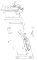
- a balancing resistor network for telephone circuits constructed in accordance with the present invention, is indicated at 10, being shown as part of a telephone circuit board (line card) 11, which is of conventional construction.
- a typical physical size of the resistor network 10 is 1.6 inches (40.6 mm) long and 0.46 inch (11.7 mm) high (mounted height). This size is for a network consisting of two balanced (matched) 100-ohm resistors.
- the indicated small resistor network satisfies all three of the above-stated levels of adverse conditions, when used in combination with a relay, and automatically re-sets so that the board 11 resumes functioning after a second-level adverse condition ceases to exist.
- the substrate is caused to have a different surface area for each size (ohmic value) or size range of resistors, the area being caused to be just sufficient that lightning transients will not cause damage to the resistors.
- Eight termination pins 14 - 21 are provided at the lower edge of resistor 10, and are respectively inserted into and connected to plated holes in the circuit board.
- Conductors 22, 23 form part of the circuit board 11 and extend respectively from central pins 17, 18 to terminals on relay 12.
- the telephone resistor and thermistor network (numbered 10 in FIGS. 1, 5 and 8) includes a thin substrate 25 that is elongate and rectangular as illustrated. It has parallel front and back surfaces that are continuous and uninterrupted, the the surfaces being sufficiently far from each other that the substrate will have much strength and also the ability to conduct substantial heat.
- the thickness of the substrate is 0.025 - 0.040 inch (0.64 - 1.02 mm).
- the substrate is a brittle ceramic, such as aluminum oxide, having a desirable moderate (not low) thermal coefficient of expansion.
- Substrate 25 has top and bottom edges 26, 27 that are parallel to each other, and end edges 28, 29 that are parallel to each other.
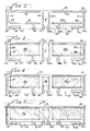
- FIG. 2 there are on the front surface of the substrate top elongate termination traces (metallisations) 31, 31a that are mirror images of each other (all mirror images being about the vertical centre line of substrate 25). Traces 31, 31a are parallel to top edge 26 and spaced a short distance therefrom. These traces respectively connect to end traces 32, 32a that are parallel to end edges 28, 29 and spaced a short distance therefrom. The indicated connections are in the upper corners of substrate 25. End traces 32, 32a are mirror images of each other.
- Lower traces 33, 33a are provided in parallel relationship to and respectively directly below top traces 31, 31a, and also in spaced parallel relationship to bottom edge 27.
- the spacing of lower traces 33, 33a above bottom edge 27 is substantial, for example about one-third of the distance between the top and bottom edges.
- Lower traces 33, 33a are mirror images of each other.
- Bottom traces are provided between the lower traces 33, 33a and bottom edge 27; these are numbered 34, 34a. They respectively connect to end traces 32, 32a, at the bottom corners of the substrate.
- the bottom traces are spaced a short distance from bottom edge 27 and are parallel to it.
- the bottom traces respectively connect to double pads 36, 37 and 36a, 37a.
- Lower traces 33, 33a respectively overlap the bottom traces and associated pads.
- the lower traces terminate at their outer ends adjacent spaces 38, 38a, such spaces being between such outer ends and the vertical traces 32, 32a.
- Near the inner ends of lower traces 33, 33a are associated vertical traces and pads 39, 39a. These connect to the lower traces 33, 33a, respectively.
- top and lower traces 31, 31a and 33, 33a are mirror images of each other and are spaced apart a relatively large distance to form a large central gap G in the substrate 25 (FIGS. 2 and 3).
- inner vertical traces 41, 41a the lower ends of which connect respectively to pads 42, 42a at the lower substrate edge.
- the traces 41, 41a are spaced from each other a substantial distance and are preferably parallel as illustrated. Traces 41, 41a are mirror images of each other as are pads 42, 42a.
- All of the above-specified traces and pads are formed of, for example, palladium silver, and are screen-printed onto the front surface of substrate 25 and then fired in a conveyor furnace. All traces, of course, have very low resistance, for example 20 milli-ohms per square.
- identical continuous thick-film resistive films 44, 44a are screen-printed onto the front surface of substrate 25 between top traces 31, 31a and lower traces 33, 33a, respectively.
- Each film 44, 44a is rectangular, and each has its upper and lower edges located in overlapping relationship to the associated traces.
- the substrate is fired in a conveyor furnace.
- Each resistive film described in this specification is an electrically conductive complex metal oxide in a glass matrix.
- the thick-film deposits are relatively thin, being deposited (screen-printed) using stainless steel screens of 250 mesh to 105 mesh (200 mesh being most common).
- the resistive film thickness ranges from 0.0004 inch to 0.0010 inch (0.01 to 0.025 mm) (fired thickness).
- thermistor film 45 there is screen-printed into the large gap G at the centre of the front surface of substrate 25 a thermistor film 45.
- Film 45 is rectangular, and the vertical edges thereof overlap inner vertical traces 41,41a.
- the thermistor film 45 is, for example, EMCA part number 4995.
- the thermistor material may be a negative temperature coefficient material in the range of -0.1%/°C to -5%/°C (ideally -1%/°C to -3%/°C), or the thermistor material may be a positive temperature coefficient material +0.1%/°C to +5%/°C (ideally +1%/°C to +3%/°C). After application of the thermistor film, the part is fired.
- an overglaze 46 is applied by screen-printing. After such application, the part is fired in order to fuse the overglaze.
- the relationships between the overglaze and the resistive films and the thermistor film are such that application and firing of the overglaze do not harm the films.
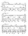
- FIGS. 6-8 the back surface of substrate 25 is shown. Except as specifically described below, everything is the same on the back surface of substrate 25 as on the front surface thereof.
- the gap at the center of the substrate, at the back thereof, is preferably somewhat smaller than gap G shown in FIGS. 2 and 3, being labelled g.
- the central gap being smaller, the resistive films are preferably somewhat longer than are the resistive films on the front surface.
- the traces and pads on the right side of the substrate (as viewed in FIG. 6), that is to say to the right of the vertical center line of substrate 25 as viewed in FIG. 6, are directly opposite and registered with the traces and pads shown at the left in FIG. 2.
- the traces and pads at the right in FIG. 6 are given the same reference numerals as those at the left in FIG. 2, except followed in each instance by the letter "b".
- the traces and pads at the left side of the substrate as viewed in FIG. 6 are registered with and correspond to the traces and pads shown at the right in FIG. 2.
- such left traces and pads are given the same reference numerals as those at the right in FIG. 2 except followed in each instance by the letter "c" instead of "a".
- resistive films 44b,44c are respectively provided directly opposite the films 44,44a shown in FIG. 3. As illustrated, the films 44b,44c extend somewhat further toward the center of the substrate 25 in that the gap g is smaller than gap G of FIGS. 2 and 3.
- the outer ends of the resistive films 44b,44c (FIG. 7) are respectively registered with the outer ends of the resistive films 44,44a shown in FIG. 3.
- Films 44b,44c are identical to each other and are substantially identical to films 44,44a.
- An arc-minimizing and environmentally protective layer is screen-printed over all of the back-side traces and resistive films, as shown in FIG. 8, and substantially corresponds to the layer shown at 46 in FIG. 5. This is glass as stated above relative to FIG. 5. Unlike the overglaze 46 shown in FIG. 5, that shown in FIG. 8 is in two sections 46a that are spaced apart at 47. However, one continuous overglaze may be provided on the back surface of the substrate, the same as on the front.
- All of the traces, films and protective arc-minimizing layers are deposited by screen-printing. In each instance, the application is followed by firing in a conveyor furnace.
- the above-indicated pins 14-21 are provided on the various pads and then secured in place and electrically connected by being dipped in solder. (A showing of the pins 14-21 is omitted in FIG. 5, but it is to be understood that they are present.) Each pin has jaws that grip opposite sides of the substrate 25 adjacent lower edge 27 thereof, that is to say grip the registered pads on such opposite sides.
- outer pin 14 grips and is electrically and physically connected to pads 36,36b; outer pin 15 to pads 37,37b; intermediate pin 16 to pads 39,39b; central pin 17 to pads 42,42b; central pin 18 to pads 42a,42c; intermediate pin 19 to pads 39a,39c; outer pin 20 to pads 37a,37c; and outer pin 21 to pads 36a,36c.
- the described traces and pins connect resistive films 44 and 44b in parallel relationship with each other, and they connect resistive films 44a and 44c in parallel relationship with each other.
- Central pins 17 and 18 connect the thermistor film 45 to conductors 22,23 on the line card 11 of FIG. 1.
- the thermistor 45 is connected to relay 12.
- Relay 12 in turn, is connected to conductors (not shown) on the circuit board that when open-circuited terminate the flow of current to the entire channel with which resistor 10 is associated, and thus to the entire resistor 10.
- the two resistive films on one side of the vertical center line of substrate 25 form one resistor, and the two resistive films on the other side of such vertical center line (other half of the substrate) form another resistor.
- the parallel connected films 44,44b form one resistor whereas the parallel-connected films 44a,44c form another resistor.
- Such one resistor and such other resistor are balanced relative to each other, that is to say are equal or substantially equal to each other in resistance value.
- the resistive films, the traces, and the substrate are such that application of a high-voltage overload to one or both of the resistors will cause substantially instantaneous breakage of the substrate and traces with consequent immediate cessation of current flow through the balancing resistor networks (or through only one of the balancing resistor networks if the overload is applied only to such one).
- the overload is typically caused by falling of a power line, etc., onto the telephone circuit, or by other contact between a power line and a telephone circuit.
- Typical overload voltages are 600 volts, 277 volts and 120 volts.
- the thermistor 45 is not spaced excessively far from the resistive films 44,44a,44b and 44c. Instead, the thermistor is sufficiently close to the films that there is conduction of sufficient heat through the substrate 25 to effect operation of the thermistor 45, which acts as a sensor for relay 12.
- the size of the substrate is correlated to the resistance values of the resistor pair, being substantially as small as permitted by having resistive films on both sides (surfaces) of the substrate.
- each resistor in the balanced resistor pair is relatively low in value. Stated more definitely, each resistor (parallel-connected resistive films on each side of the vertical center line of the substrate) has a resistance in the range of about 25 ohms to about 300 ohms.
- a further important relationship is that there is no trace (or traces) spaced upwardly above the top edges of the resistive films 44,44a,44b,44c.
- the upper region of a substrate is therefor very effectively and efficiently used as a support for the resistive films, which reduces substrate size.
- the lower traces 33,33a,33b and 33c are spaced substantial distances upwardly from the bottom edge 27 of the substrate, in order to provide (in combination with the overglaze) isolation relative to the termination pins and pads.
- resistive films are each substantially continuous, by which it is meant that substantially all of the substrate area beneath each resistive film--between opposed traces-- has resistive film deposited thereon. This relationship creates greater stability of resistance value under lightning transient conditions.
- the particular resistor 10 may be the one having the physical size stated above (namely, 1.6 inch (40.6 mm) long by 0.46 inch (1.7 mm) high), with each resistor having a value of 100 ohms.
- the parallel-connected films on one side of the vertical centre line of the substrate have a combined value of 100 ohms
- the parallel-connected films on the other side of the vertical centre line of the substrate have a combined value of 100 ohms.
- first-level condition namely a lightning transient. Because the resistive films are on both sides of the substrate, and despite the small size of the substrate, the resistive films are not damaged. In other words, this transient condition is survivable. Current flow through the resistor and through the circuit board is not interrupted or discontinued, and nothing is harmed.
- first-level condition Another type of first-level condition is where a technician has created faulty wiring, but the faulty wiring happens to be of a type that does not result in generation of sufficient heat in the resistor network to operate thermistor 45 in a way that operates the relay 12 and thus discontinues or interrupts current flow.
- Another type of first-level condition is where a technician has created faulty wiring of a type such that sufficient heat is generated to effect operation of the relay. With such a first-level condition, the thermistor-relay combination makes it survivable in that the relay will automatically reset. The same occurs relative to a second-level condition, as next described.
- a second-level condition For example, let it be assumed that a particular type of faulty wiring is created by a technician, and that the particular type is one which tends to cause excessive heating of the resistor network and/or of components on circuit board (line card) 11.
- the heating may be such as to tend to effect melting of, burning of, or other harm to synthetic resin-cased components on the circuit board or to the.circuit board itself.
- sufficient heat is conducted through substrate 25 from resistive films 44,44a,44b and 44c to thermistor film 45 that the resistance of the latter changes in such manner as to effect operation of relay 12 to open the circuit in the particular channel in which the resistor-relay pair 10,12 is mounted.
- the thermistor film 45 has such a resistance that the associated relay 12 operates to close the circuit through the channel in which the resistor-relay pair 10,12 is mounted. In other words, the thermistor resets without human intervention. It is to be understood that a time-delay network may be built into the relay 12 to delay the time at which such resetting occurs. As another option, the relay may have a zero crossing circuit to minimize arcing at the relay contacts.
- a 600-volt power line may contact the telephone line of the channel with which the resistor-relay pair 10,12 is associated.
- a sudden overload current present in the resistive films 44,44a,44b and 44c which causes very rapid heating of the substrate material sandwiched between the two films of each resistor.
- the substrate material at the ends of the substrate is not thus rapidly heated but instead remains (in comparison to the temperatures present between the films in each film pair) relatively cool. There is thus a thermal shock at each end of the substrate, and this causes breaking at the substrate at the corners and/or ends thereof.
- traces 32,32a,32b and 32c are at places where the substrate is broken, these traces are immediately interrupted so that the current flow through resistor 10, and thus the ⁇ circuit board, stops. This occurs in a very small fraction of a second.
- the overglaze 46 performs important functions of aiding in minimizing arcing. Any arcing stops so very fast that small wires in the telephone system do not melt, become damaged, or burn.
- resistor and resistor combination with a relay, particularly adapted and effective for small-size substrates, and for those companies (and applications) where automatic resetting after cessation of a second-level adverse condition is desired.
- the resistor is small, strong, environmentally protected, etc. It and the associated relay do the desired job reliably relative to all three levels of adverse conditions, and reset automatically after a second-level adverse condition (and after a circuit-interrupting type of first-level condition) has existed.
Landscapes
- Engineering & Computer Science (AREA)
- Signal Processing (AREA)
- Microelectronics & Electronic Packaging (AREA)
- Telephone Function (AREA)
- Thermistors And Varistors (AREA)
- Emergency Protection Circuit Devices (AREA)
- Apparatuses And Processes For Manufacturing Resistors (AREA)
Claims (9)
- Carte de circuit de téléphone (11) avec une combinaison d'un réseau de résistances d'équilibrage et de coupure comprenant un substrat fin (25) présentant des surfaces avant et arrière parallèles l'une à l'autre;
un premier (44) et un deuxième (44a) films résistifs à film épais imprimés par sérigraphie sur la dite surface avant du dit substrat;
un troisième (44b) et un quatrième (44c) films résistifs à film épais imprimés par sérigraphie sur la dite surface arrière du dit substrat (25), les dits premier et deuxième films résistifs (44, 44a) se trouvant respectivement sur les côtés gauche et droit de la dite surface avant, et étant séparés l'un de l'autre par un espace (G), les dits quatrième et troisième films résistifs (44c, 44b) se trouvant respectivement sur les côtés gauche et droit de la dite surface arrière et étant séparés l'un de l'autre, les dits premier (44) et troisième (44b) films résistifs étant généralement en registre l'un avec l'autre, et les dits premier (44) et troisième (44b) films résistifs étant connectés électriquement l'un à l'autre et formant une première résistance, les dits deuxième (44a) et quatrième (44c) films résistifs étant connectés électriquement l'un à l'autre et formant une autre résistance, la dite première résistance et la dite autre résistance présentant des résistances telles qu'elles soient en équilibre l'une avec l'autre;
des moyens de connexion (14, 15, 16, 19, 20, 21) pour connecter la dite première résistance et la dite autre résistance à la carte de circuit de téléphone (11);
des moyens (46) de revêtement appliqués sur les dits films pour la protection de l'environnement et pour minimiser des arcs;
le dit substrat (25) et les dits films résistifs (44, 44a, 44b, 44c) ayant une dimension physique telle que ni les dits films, ni le dit substrat ne seront endommagé par des transitoires de la foudre;
caractérisé en ce qu'un film à thermistance (45) est imprimé par sérigraphie sur la dite surface avant du dit substrat dans le dit espace (G);
des moyens de connexion (17, 18) raccordent le dit film à thermistance (45) au dit circuit (11);
un relais (12) est monté sur la dite carte de circuit (11) et est connecté électriquement aux dits moyens de connexion (17, 18) mentionnés en dernier, et
dans lequel le dit relais (12), le dit film à thermistance (45) et les dits films résistifs (44, 44a, 44b, 44c) sont en relation l'un avec l'autre de manière telle que le dit film à thermistance (45) provoquera le fonctionnement du dit relais (12) lorsque le dit substrat (25) commence à s'échauffer de manière excessive suite à une mauvaise connexion d'un type qui augmente nettement le débit de courant. - L'invention telle que revendiquée dans la revendication 1, dans laquelle les dits moyens de connexion pour la dite première résistance et la dite autre résistance comprennent des pistes de connexion (32, 32a, 32b, 32c) sur les régions d'extrémités des dites surfaces de substrat et séparées des dits films résistifs (44), les dites pistes (32) étant adaptées pour se casser essentiellement instantanément lorsque les dites régions d'extrémités se brisent suite à une haute tension appliquée à au moins l'une des dites résistance équilibrées, le dit film à thermistance (45) étant localisé de manière à ne pas provoquer d'arc vers les dits films résistifs lorsque la dite haute tension est appliquée.
- L'invention telle que revendiquée dans la revendication 1 ou 2, dans laquelle le dit substrat (25) est allongé, et chacun des films résistifs (44) est généralement de configuration rectangulaire.
- L'invention telle que revendiquée dans l'une quelconque des revendications précédentes, dans laquelle chacun des dits films résistifs (44) est continu.
- L'invention telle que revendiquée dans l'une quelconque des revendications précédentes, dans laquelle le dit film à thermistance (45) est espacé suffisamment loin des dits films résistifs, et le dit moyen de revêtement (46) est tel qu'il y ait un risque minimal de formation d'un arc entre les dits films resistifs (44) et le dit film à thermistance (45) lorsqu'une surcharge de haute tension est appliquée aux dits films résistifs (44).
- L'invention telle que revendiquée dans l'une quelconque des revendications précédentes, dans laquelle la dimension physique du dit substrat (25) n'est suffisamment grande que pour que les dits films (44) ne soient pas endommagés par des transitoires de la foudre.
- L'invention telle que revendiquée dans l'une quelconque des revendications précédentes comprenant en outre:des pistes métallisées, allongées, supérieures, gauche (31) et droite (31a), imprimées par sérigraphie sur la dite surface avant, généralement alignées l'une par rapport à l'autre, les dites pistes gauche (31) et droite (31a) se trouvant respectivement sur les côtés gauche et droit d'un axe vertical du dit substrat;des pistes métallisées, allongées, inférieures, gauche (33) et droite (33a), imprimées par sérigraphie sur la dite surface avant, généralement alignées l'une par rapport à l'autre, les dites pistes inférieures gauche (33) et droite (33a) se trouvant respectivement sur les côtés gauche et droit du dit axe vertical, les dites pistes inférieures gauche (33) et droite (33a) étant respectivement séparées par des distances relativement grandes en-dessous des dites pistes supérieures gauche (31) et droite (31a),le dit premier film résistif (44) s'étendant entre les dites pistes gauche supérieure (31) et gauche inférieure (33), le dit deuxième film résistif (44a) s'étendant entre les dites pistes droite supérieure (31a) et droite inférieure (33a);le dit substrat (25) ayant des bords supérieur (26) et inférieur (27) essentiellement parallèles l'un à l'autre, et des bords d'extrémités gauche (28) et droit (29) essentiellement parallèles l'un à l'autre;les dites pistes de connexion (32, 32a, 32b, 32c) comprennent des pistes métallisées d'extrémités gauche (32) et droite (32a) imprimées par sérigraphie sur la dite surface avant, la dite piste d'extrémité gauche (32) étant connectée à la dite piste supérieure gauche (31) et étant située entre le dit bord d'extrémité gauche (28) du dit substrat (25) et le bord d'extrémité gauche du dit premier film résistif (44), la dite piste d'extrémité droite (32a) étant connectée à la dite piste supérieure droite (31a) et étant située entre le dit bord d'extrémité droit (29) du dit substrat (25) et le bord d'extrémité droit du dit deuxième film résistif (44a); etdes pistes métallisées inférieures gauche (34) et droite (34a) imprimées par sérigraphie sur la dite surface avant près du bord inférieur (27) du dit substrat (25), dans une relation d'espacement en-dessous des dites pistes inférieures, les dites pistes inférieures gauche (34) et droite (34a) étant connectées respectivement à la dite piste d'extrémité gauche (32) et à la dite piste d'extrémité droite (32a).
- L'invention telle que revendiquée dans la revendication 7, dans laquelle les dites pistes supérieures (31) sont relativement proches de, et parallèles au dit bord supérieur (26) du dit substrat (25), et dans laquelle il n'y a pas de pistes entre le dit bord supérieur (26) et les dites pistes supérieures (31).
- L'invention telle que revendiquée dans l'une quelconque des revendications précédentes, dans laquelle les dits moyens de connexion (14, 15, 16, 19, 20, 21) pour connecter la dite première résistance et la dite autre résistance à la carte de circuit de téléphone (11) comprennent:des broches de connexion gauches et droites (14, 15, 20, 21) aux dits bords inférieurs (27) du dit substrat (25) et connectées respectivement aux dites pistes inférieures gauche (34) et droite (34a); etdes première et deuxième broches de connexion intermédiaires (16, 19) aux dits bords inférieurs (27) et connectées respectivement aux dits premier (44) et deuxième (44a) films résistifs dans des régions de ceux-ci éloignées des dites pistes gauche (32) et droite (32a).
Applications Claiming Priority (4)
| Application Number | Priority Date | Filing Date | Title |
|---|---|---|---|
| US558993A | 1993-01-19 | 1993-01-19 | |
| US5589 | 1993-01-19 | ||
| US08/037,927 US5361300A (en) | 1993-01-19 | 1993-03-26 | Balancing resistor and thermistor network for telephone circuits, and combination thereof with relay |
| US37927 | 2001-10-19 |
Publications (3)
| Publication Number | Publication Date |
|---|---|
| EP0608077A2 EP0608077A2 (fr) | 1994-07-27 |
| EP0608077A3 EP0608077A3 (fr) | 1995-03-22 |
| EP0608077B1 true EP0608077B1 (fr) | 2002-05-02 |
Family
ID=26674513
Family Applications (1)
| Application Number | Title | Priority Date | Filing Date |
|---|---|---|---|
| EP94300262A Expired - Lifetime EP0608077B1 (fr) | 1993-01-19 | 1994-01-14 | Réseau de résistances comprenant des circuits téléphoniques |
Country Status (4)
| Country | Link |
|---|---|
| US (1) | US5361300A (fr) |
| EP (1) | EP0608077B1 (fr) |
| AT (1) | ATE217116T1 (fr) |
| DE (1) | DE69430497T2 (fr) |
Families Citing this family (6)
| Publication number | Priority date | Publication date | Assignee | Title |
|---|---|---|---|---|
| US5914648A (en) | 1995-03-07 | 1999-06-22 | Caddock Electronics, Inc. | Fault current fusing resistor and method |
| SE509341C2 (sv) * | 1996-02-01 | 1999-01-11 | Ericsson Telefon Ab L M | Telefonväxelanpassad linjekretskoppling |
| US5889462A (en) * | 1996-04-08 | 1999-03-30 | Bourns, Inc. | Multilayer thick film surge resistor network |
| US8254142B2 (en) | 2009-09-22 | 2012-08-28 | Wintec Industries, Inc. | Method of using conductive elastomer for electrical contacts in an assembly |
| US8593825B2 (en) * | 2009-10-14 | 2013-11-26 | Wintec Industries, Inc. | Apparatus and method for vertically-structured passive components |
| US11636993B2 (en) | 2019-09-06 | 2023-04-25 | Eaton Intelligent Power Limited | Fabrication of printed fuse |
Family Cites Families (19)
| Publication number | Priority date | Publication date | Assignee | Title |
|---|---|---|---|---|
| SE341746B (fr) * | 1970-03-10 | 1972-09-18 | Ericsson Telefon Ab L M | |
| US3778744A (en) * | 1973-02-28 | 1973-12-11 | H Brandi | Film resistors |
| GB1466569A (en) * | 1973-10-05 | 1977-03-09 | Erie Electronics Ltd | Resistors |
| US4041440A (en) * | 1976-05-13 | 1977-08-09 | General Motors Corporation | Method of adjusting resistance of a thick-film thermistor |
| DE2651071B2 (de) * | 1976-11-09 | 1980-03-20 | Licentia Patent-Verwaltungs-Gmbh, 6000 Frankfurt | Verfahren zur Herstellung eines abgeglichenen Widerstandes in Dickschichttechnik |
| US4297670A (en) * | 1977-06-03 | 1981-10-27 | Angstrohm Precision, Inc. | Metal foil resistor |
| DE3245629A1 (de) * | 1982-12-09 | 1984-06-14 | Telefunken electronic GmbH, 6000 Frankfurt | Sicherungselement mit einer dickschichtwiderstandsanordnung |
| US4528546A (en) * | 1983-05-02 | 1985-07-09 | National Semiconductor Corporation | High power thick film |
| US4467310A (en) * | 1983-10-03 | 1984-08-21 | Northern Telecom Limited | Telephone subscriber line battery feed resistor arrangements |
| FR2562711B1 (fr) * | 1984-04-10 | 1987-01-23 | Renix Electronique Sa | Resistance haute tension de precision a faible encombrement en technologie couches epaisses |
| GB2163307B (en) * | 1984-08-15 | 1987-12-16 | Crystalate Electronics | Fusible electrical resistor |
| US4809324A (en) * | 1987-07-27 | 1989-02-28 | Siemens Transmission Systems, Inc. | Subscriber line interface circuit (SLIC) isolation from lighting-induced ground overshoots |
| JPH01220403A (ja) * | 1988-02-26 | 1989-09-04 | Murata Mfg Co Ltd | ケース内蔵型の正特性サーミスタ |
| US4959751A (en) * | 1988-08-16 | 1990-09-25 | Delco Electronics Corporation | Ceramic hybrid integrated circuit having surface mount device solder stress reduction |
| US4961065A (en) * | 1989-03-27 | 1990-10-02 | Cts Corporation | Fail-safe resistor |
| GB2230921B (en) * | 1989-04-25 | 1994-01-05 | Plessey Telecomm | Protective arrangement for telecommunications line interface circuit |
| US5204799A (en) * | 1990-03-22 | 1993-04-20 | Gpt Limited | Protective arrangement for telecommunications line interface circuit |
| ATE174154T1 (de) * | 1991-04-02 | 1998-12-15 | Caddock Electronics Inc | Widerstand, der imstande ist, als überlastschalter zu agieren |
| US5254969A (en) * | 1991-04-02 | 1993-10-19 | Caddock Electronics, Inc. | Resistor combination and method |
-
1993
- 1993-03-26 US US08/037,927 patent/US5361300A/en not_active Expired - Lifetime
-
1994
- 1994-01-14 DE DE69430497T patent/DE69430497T2/de not_active Expired - Lifetime
- 1994-01-14 AT AT94300262T patent/ATE217116T1/de not_active IP Right Cessation
- 1994-01-14 EP EP94300262A patent/EP0608077B1/fr not_active Expired - Lifetime
Also Published As
| Publication number | Publication date |
|---|---|
| ATE217116T1 (de) | 2002-05-15 |
| EP0608077A3 (fr) | 1995-03-22 |
| DE69430497T2 (de) | 2002-10-10 |
| DE69430497D1 (de) | 2002-06-06 |
| EP0608077A2 (fr) | 1994-07-27 |
| US5361300A (en) | 1994-11-01 |
Similar Documents
| Publication | Publication Date | Title |
|---|---|---|
| US4494104A (en) | Thermal Fuse | |
| JP5259289B2 (ja) | 一体化されたサーミスタ及び金属素子装置並びに方法 | |
| EP0017324B1 (fr) | Dispositif dérivant les surtensions avec un dispositif protecteur contre les pannes | |
| TWI390568B (zh) | Protection element | |
| US3978443A (en) | Fusible resistor | |
| NL8006411A (nl) | Inrichting voor het beveiligen tegen oververhitting door overspanning van een spanningsbegrenzende schakeling. | |
| US5204799A (en) | Protective arrangement for telecommunications line interface circuit | |
| US5361300A (en) | Balancing resistor and thermistor network for telephone circuits, and combination thereof with relay | |
| US6614341B2 (en) | Thick film circuit with fuse | |
| US5254969A (en) | Resistor combination and method | |
| CN1132195C (zh) | 具有过载保护的混合电路装置 | |
| CA1187917A (fr) | Fusible thermique | |
| EP0395231B1 (fr) | Disposition de protection pour circuit d'interface de ligne de télécommunications | |
| US10204757B2 (en) | Electrical circuit protection device with high resistive bypass material | |
| EP0507465B1 (fr) | Résistance capable d'agiter comme un disjoncteur | |
| CN104658724A (zh) | 用于压敏变阻器的多触点元件及压敏变阻器 | |
| EP0682347B1 (fr) | Résistance de téléphone | |
| JPH1197215A (ja) | バリスタおよびバリスタ内蔵電源装置 | |
| JP2528404B2 (ja) | 回路開放素子 | |
| JP2584370B2 (ja) | 過電圧防止素子 | |
| JPH0733353Y2 (ja) | ヒューズ抵抗器 | |
| JPH114535A (ja) | 保護用回路及び複合型保護用デバイス | |
| JPH0568337A (ja) | 回路開放素子及び過電圧過電流防止素子 | |
| JPS5858703A (ja) | セラミツクバリスタ | |
| JPH0733352Y2 (ja) | ヒューズ抵抗器 |
Legal Events
| Date | Code | Title | Description |
|---|---|---|---|
| PUAI | Public reference made under article 153(3) epc to a published international application that has entered the european phase |
Free format text: ORIGINAL CODE: 0009012 |
|
| AK | Designated contracting states |
Kind code of ref document: A2 Designated state(s): AT BE CH DE ES FR GB IE IT LI NL PT SE |
|
| PUAL | Search report despatched |
Free format text: ORIGINAL CODE: 0009013 |
|
| AK | Designated contracting states |
Kind code of ref document: A3 Designated state(s): AT BE CH DE ES FR GB IE IT LI NL PT SE |
|
| 17P | Request for examination filed |
Effective date: 19950908 |
|
| 17Q | First examination report despatched |
Effective date: 19990804 |
|
| GRAG | Despatch of communication of intention to grant |
Free format text: ORIGINAL CODE: EPIDOS AGRA |
|
| GRAG | Despatch of communication of intention to grant |
Free format text: ORIGINAL CODE: EPIDOS AGRA |
|
| GRAH | Despatch of communication of intention to grant a patent |
Free format text: ORIGINAL CODE: EPIDOS IGRA |
|
| REG | Reference to a national code |
Ref country code: GB Ref legal event code: IF02 |
|
| GRAH | Despatch of communication of intention to grant a patent |
Free format text: ORIGINAL CODE: EPIDOS IGRA |
|
| GRAA | (expected) grant |
Free format text: ORIGINAL CODE: 0009210 |
|
| AK | Designated contracting states |
Kind code of ref document: B1 Designated state(s): AT BE CH DE ES FR GB IE IT LI NL PT SE |
|
| PG25 | Lapsed in a contracting state [announced via postgrant information from national office to epo] |
Ref country code: NL Free format text: LAPSE BECAUSE OF FAILURE TO SUBMIT A TRANSLATION OF THE DESCRIPTION OR TO PAY THE FEE WITHIN THE PRESCRIBED TIME-LIMIT Effective date: 20020502 Ref country code: LI Free format text: LAPSE BECAUSE OF FAILURE TO SUBMIT A TRANSLATION OF THE DESCRIPTION OR TO PAY THE FEE WITHIN THE PRESCRIBED TIME-LIMIT Effective date: 20020502 Ref country code: IT Free format text: LAPSE BECAUSE OF FAILURE TO SUBMIT A TRANSLATION OF THE DESCRIPTION OR TO PAY THE FEE WITHIN THE PRE;WARNING: LAPSES OF ITALIAN PATENTS WITH EFFECTIVE DATE BEFORE 2007 MAY HAVE OCCURRED AT ANY TIME BEFORE 2007. THE CORRECT EFFECTIVE DATE MAY BE DIFFERENT FROM THE ONE RECORDED.SCRIBED TIME-LIMIT Effective date: 20020502 Ref country code: FR Free format text: LAPSE BECAUSE OF FAILURE TO SUBMIT A TRANSLATION OF THE DESCRIPTION OR TO PAY THE FEE WITHIN THE PRESCRIBED TIME-LIMIT Effective date: 20020502 Ref country code: CH Free format text: LAPSE BECAUSE OF FAILURE TO SUBMIT A TRANSLATION OF THE DESCRIPTION OR TO PAY THE FEE WITHIN THE PRESCRIBED TIME-LIMIT Effective date: 20020502 Ref country code: BE Free format text: LAPSE BECAUSE OF FAILURE TO SUBMIT A TRANSLATION OF THE DESCRIPTION OR TO PAY THE FEE WITHIN THE PRESCRIBED TIME-LIMIT Effective date: 20020502 Ref country code: AT Free format text: LAPSE BECAUSE OF FAILURE TO SUBMIT A TRANSLATION OF THE DESCRIPTION OR TO PAY THE FEE WITHIN THE PRESCRIBED TIME-LIMIT Effective date: 20020502 |
|
| REF | Corresponds to: |
Ref document number: 217116 Country of ref document: AT Date of ref document: 20020515 Kind code of ref document: T |
|
| REG | Reference to a national code |
Ref country code: GB Ref legal event code: FG4D |
|
| REG | Reference to a national code |
Ref country code: CH Ref legal event code: EP |
|
| REF | Corresponds to: |
Ref document number: 69430497 Country of ref document: DE Date of ref document: 20020606 |
|
| REG | Reference to a national code |
Ref country code: IE Ref legal event code: FG4D |
|
| PG25 | Lapsed in a contracting state [announced via postgrant information from national office to epo] |
Ref country code: SE Free format text: LAPSE BECAUSE OF FAILURE TO SUBMIT A TRANSLATION OF THE DESCRIPTION OR TO PAY THE FEE WITHIN THE PRESCRIBED TIME-LIMIT Effective date: 20020802 Ref country code: PT Free format text: LAPSE BECAUSE OF FAILURE TO SUBMIT A TRANSLATION OF THE DESCRIPTION OR TO PAY THE FEE WITHIN THE PRESCRIBED TIME-LIMIT Effective date: 20020802 |
|
| NLV1 | Nl: lapsed or annulled due to failure to fulfill the requirements of art. 29p and 29m of the patents act | ||
| REG | Reference to a national code |
Ref country code: CH Ref legal event code: PL |
|
| PG25 | Lapsed in a contracting state [announced via postgrant information from national office to epo] |
Ref country code: ES Free format text: LAPSE BECAUSE OF FAILURE TO SUBMIT A TRANSLATION OF THE DESCRIPTION OR TO PAY THE FEE WITHIN THE PRESCRIBED TIME-LIMIT Effective date: 20021128 |
|
| EN | Fr: translation not filed | ||
| PG25 | Lapsed in a contracting state [announced via postgrant information from national office to epo] |
Ref country code: IE Free format text: LAPSE BECAUSE OF NON-PAYMENT OF DUE FEES Effective date: 20030114 |
|
| PLBE | No opposition filed within time limit |
Free format text: ORIGINAL CODE: 0009261 |
|
| STAA | Information on the status of an ep patent application or granted ep patent |
Free format text: STATUS: NO OPPOSITION FILED WITHIN TIME LIMIT |
|
| 26N | No opposition filed |
Effective date: 20030204 |
|
| REG | Reference to a national code |
Ref country code: IE Ref legal event code: MM4A |
|
| PGFP | Annual fee paid to national office [announced via postgrant information from national office to epo] |
Ref country code: DE Payment date: 20110112 Year of fee payment: 18 |
|
| PGFP | Annual fee paid to national office [announced via postgrant information from national office to epo] |
Ref country code: GB Payment date: 20110112 Year of fee payment: 18 |
|
| GBPC | Gb: european patent ceased through non-payment of renewal fee |
Effective date: 20120114 |
|
| PG25 | Lapsed in a contracting state [announced via postgrant information from national office to epo] |
Ref country code: DE Free format text: LAPSE BECAUSE OF NON-PAYMENT OF DUE FEES Effective date: 20120801 Ref country code: GB Free format text: LAPSE BECAUSE OF NON-PAYMENT OF DUE FEES Effective date: 20120114 |
|
| REG | Reference to a national code |
Ref country code: DE Ref legal event code: R119 Ref document number: 69430497 Country of ref document: DE Effective date: 20120801 |