EP0608151A2 - Ladungspumpenschaltung mit hoher Geschwindigkeit und wenig Drift - Google Patents
Ladungspumpenschaltung mit hoher Geschwindigkeit und wenig Drift Download PDFInfo
- Publication number
- EP0608151A2 EP0608151A2 EP94300491A EP94300491A EP0608151A2 EP 0608151 A2 EP0608151 A2 EP 0608151A2 EP 94300491 A EP94300491 A EP 94300491A EP 94300491 A EP94300491 A EP 94300491A EP 0608151 A2 EP0608151 A2 EP 0608151A2
- Authority
- EP
- European Patent Office
- Prior art keywords
- output
- current
- input stage
- input
- coupled
- Prior art date
- Legal status (The legal status is an assumption and is not a legal conclusion. Google has not performed a legal analysis and makes no representation as to the accuracy of the status listed.)
- Granted
Links
Images




Classifications
-
- G—PHYSICS
- G05—CONTROLLING; REGULATING
- G05F—SYSTEMS FOR REGULATING ELECTRIC OR MAGNETIC VARIABLES
- G05F3/00—Non-retroactive systems for regulating electric variables by using an uncontrolled element, or an uncontrolled combination of elements, such element or such combination having self-regulating properties
- G05F3/02—Regulating voltage or current
- G05F3/08—Regulating voltage or current wherein the variable is DC
- G05F3/10—Regulating voltage or current wherein the variable is DC using uncontrolled devices with non-linear characteristics
- G05F3/16—Regulating voltage or current wherein the variable is DC using uncontrolled devices with non-linear characteristics being semiconductor devices
- G05F3/20—Regulating voltage or current wherein the variable is DC using uncontrolled devices with non-linear characteristics being semiconductor devices using diode- transistor combinations
- G05F3/22—Regulating voltage or current wherein the variable is DC using uncontrolled devices with non-linear characteristics being semiconductor devices using diode- transistor combinations wherein the transistors are of the bipolar type only
-
- H—ELECTRICITY
- H02—GENERATION; CONVERSION OR DISTRIBUTION OF ELECTRIC POWER
- H02M—APPARATUS FOR CONVERSION BETWEEN AC AND AC, BETWEEN AC AND DC, OR BETWEEN DC AND DC, AND FOR USE WITH MAINS OR SIMILAR POWER SUPPLY SYSTEMS; CONVERSION OF DC OR AC INPUT POWER INTO SURGE OUTPUT POWER; CONTROL OR REGULATION THEREOF
- H02M3/00—Conversion of DC power input into DC power output
- H02M3/02—Conversion of DC power input into DC power output without intermediate conversion into AC
- H02M3/04—Conversion of DC power input into DC power output without intermediate conversion into AC by static converters
- H02M3/06—Conversion of DC power input into DC power output without intermediate conversion into AC by static converters using resistors or capacitors, e.g. potential divider
- H02M3/07—Conversion of DC power input into DC power output without intermediate conversion into AC by static converters using resistors or capacitors, e.g. potential divider using capacitors charged and discharged alternately by semiconductor devices with control electrode, e.g. charge pumps
-
- H—ELECTRICITY
- H03—ELECTRONIC CIRCUITRY
- H03L—AUTOMATIC CONTROL, STARTING, SYNCHRONISATION OR STABILISATION OF GENERATORS OF ELECTRONIC OSCILLATIONS OR PULSES
- H03L7/00—Automatic control of frequency or phase; Synchronisation
- H03L7/06—Automatic control of frequency or phase; Synchronisation using a reference signal applied to a frequency- or phase-locked loop
- H03L7/08—Details of the phase-locked loop
- H03L7/085—Details of the phase-locked loop concerning mainly the frequency- or phase-detection arrangement including the filtering or amplification of its output signal
- H03L7/089—Details of the phase-locked loop concerning mainly the frequency- or phase-detection arrangement including the filtering or amplification of its output signal the phase or frequency detector generating up-down pulses
- H03L7/0891—Details of the phase-locked loop concerning mainly the frequency- or phase-detection arrangement including the filtering or amplification of its output signal the phase or frequency detector generating up-down pulses the up-down pulses controlling source and sink current generators, e.g. a charge pump
- H03L7/0895—Details of the current generators
- H03L7/0896—Details of the current generators the current generators being controlled by differential up-down pulses
Definitions
- This invention relates to a charge pump circuit commonly used in phase-locked loop circuits. More particularly, the present invention relates to a charge pump topology utilizing non-complementary bipolar processes that is suitable for a monolithic integrated circuit implementation.
- a charge pump is an electronic circuit block which is commonly used in phase-locked loop circuits.
- a phase-locked loop is a frequency-selective device comprising a phase detector, a loop filter, an amplifier, and a voltage controlled oscillator(VCO) interconnected in known manner to form a feedback system.
- the charge pump converts the logic level pulses generated by the phase detector into current pulses which are fed to the loop filter.
- the loop filter integrates the current pulses to produce a control voltage for the voltage controlled oscillator.
- the logic level pulses used by the charge pump are commonly referred to as "PUMP UP” or “UP” pulses and “PUMP DOWN” or “DOWN” pulses.
- the charge pump produces an output current 1 0 .
- the output current 1 0 is generated according to a logic truth table comprising the "PUMP UP” and “PUMP DOWN” logic pulses.
- the total charge supplied to the loop filter by the charge pump be an accurate reflection of the pulse widths of the UP and DOWN logic signals.
- the charge produced by the charge pump should be I*T UP coulombs.
- the charge pump should produce a charge of - I * T DOWN coulombs.
- the pulses of output current 1 0 cannot be perfectly square due to the limitations of non-zero rise and fall times. Thus, the actual charge supplied by the charge pump to the loop filter will be less than the ideal quantity discussed above.
- the practical charge pump should exhibit fast response time, symmetrical response to the input logic level pulses, and virtually zero idle state output leakage current.
- the present invention provides a device for converting binary logic pulses into an output current, the output current being switchable between a positive and a negative polarity, said device comprising: (a) a first input stage for inputting a first binary logic pulse, said first input stage having an output and means for generating a first current component at said output in response to said first binary logic pulse; (b) a second input stage for inputting a second binary logic pulse, said second input stage having an output and means for generating a second current at the output of said second input stage in response to said second binary logic pulse; (c) current drive means for producing and controlling a third current component, said current drive means being coupled to the output of said first input stage; and (d) commutating means for producing the output current from said first, second and third current components, said commutating means including first and second switches said first and second switches being coupled to each other and being coupled to the output of said first input stage and to the output of said second input stage, said commutating means including an output port coupled to
- FIG 1 shows a standard phase-locked loop circuit.
- the phase-locked loop (PLL) is one of the fundamental circuit blocks of communications systems.
- the PLL is a frequency-selective circuit comprising a phase detector 10, a loop filter 12, an amplifier 14, and a voltage controlled oscillator 16.
- the phase detector 10, the loop filter 12, and the amplifier 14 are connected to a form feedback system with the voltage controlled oscillator 16.
- a charge pump 18 according to the present invention is incorporated into the phase detector 10 to convert logic level pulses generated by the phase detector 10 into an output current 1 0 (current pulses) which are then fed to the loop filter 12.
- the charge pump topology 18 utilizes only NPN devices for current switching, and therefore is well suited for a monolithic integrated circuit implementation.
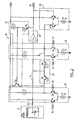
- the charge pump topology 18 according to the present invention comprises an UP logic pulse input stage 20, a DOWN logic pulse input stage 22, a commutating stage 24, a buffer stage 26, a clamping circuit 28, a current drive stage 30, a loop fi Iter output terminal 32 and a voltage controlled oscillator input terminal 34.
- the output terminal 32 allows the charge pump 18 (and output current 1 0 ) to be coupled to the loop filter 12.
- the loop filter 12 typically includes an integrating capacitor C which converts the output current 1 0 from the charge pump 18 into a voltage signal for controlling the voltage controlled oscillator stage 16.
- the UP pulse input stage 20 comprises a pair of NPN transistors Q 1 and Q 2 , which are emitter coupled to form a differential pair current switch.
- the emitter-coupled transistor topology offers high speed operation because the transistors do not operate in the saturation region.
- the base of the first transistor Q 1 provides a non-inverted UP logic pulse input terminal 36
- the base of the second transistor Q 2 is an input terminal 38 for the inverted UP (UP * ) logic pulse input.
- the input stage 20 includes a current source 1 1 and a current sink I 2 .
- Current source 1 1 connects to the collector of transistor Q 2 and produces an internal current I.
- Current sink 1 2 connects to the coupled emitters of transistors Q 1 and Q 2 and sinks a current (21) which flows in the emitters of the two transistors Q 1 and Q 2 when they are switched on.
- the collector of transistor Q 2 provides an output for the UP pulse input stage 20.
- the DOWN pulse input stage 22 is very similar to the UP pulse input stage 20 described above.
- the DOWN pulse input stage 22 comprises two transistors Q 3 and Q 4 which are also emitter-coupled to form a differential pair current switch.
- the base of transistor Q 3 provides an input 40 for the non-inverted DOWN pulse
- the base of transistor Q 4 provides an input 42 for the inverted DOWN pulse.
- the DOWN input stage 22 also includes a current source 1 3 and a current sink 1 4 .
- the current source 1 3 connects to the collector of transistor Q 3 and produces an internal current I which flows into the collector of transistor Q 3 .
- the current sink 1 4 connects to the coupled emitters of transistors Q 3 and Q 4 and sinks a current 21 which flows from the emitters of the transistors Q 3 and Q 4 .
- the collector of transistor Q 3 provides an output from the DOWN pulse input stage 22.
- the commutating stage 24 comprises two diodes which can be formed from two diode-connected transistors Q 5 and Q 6 .
- the two diode-connected transistors Q 5 and Q 6 are coupled between the collector of transistor Q 2 and the collector of transistor Q 3 .
- the anode of diode Q 5 is connected to the collector of transistor Q 2 and the cathode of di- odeis connected to the anode of diode Q 6 .
- the cathode of diode Q 5 is connected to the collector of transistor Q 3 .
- the loop filter output terminal 32 connects to the node formed by the connection of the cathode of diode Q 5 and the anode of diode Q 6
- the current drive stage 30 comprises a drive transistor Q 10 , a current source 1 6 and a diode-connected transistor Q 9 (diode Q 9 ).
- the emitter of the drive transistor Q 10 is connected to the collector of transistor Q 2 and the anode of diode Q 5 , and the collector of transistor Q 10 is connected to the positive supply rail V cc .
- the base of transistor Q lo is connected to the anode of diode Q 9 and the output of the current source 1 6 .
- the current source 1 6 produces a current I which as will be explained is used to generate the output current 1 0 .
- the cathode of diode Q 9 is connected to the voltage controlled oscillator terminal 34 and the output of the buffer stage 26.
- the buffer stage 26 is connected between the loop fi lter output 32 and the VCO terminal 34.
- the buffer stage 26 comprises a unity gain amplifier 44 having a very high input impedance.
- the function of the buffer stage 26 is to buffer the voltage level on the filter output 32 for use by the drive stage 30 and the clamping circuit 28 to limit the voltage swing across the diodes Q 5 and Q 6 in the commutating stage 24.
- the clamping circuit 28 is coupled between the collector of transistor Q 3 (i.e. the output of the DOWN pulse input stage) and output of the buffer stage 26 as shown in Figure 2.
- the function of the clamping circuit 28 is to limit the voltage swing across the diodes Q 5 and Q 6 to a voltage of one V BE where V BE is the forward voltage drop across a base-emitter junction.
- the clamping circuit 28 comprises a diode-connected transistor Q 7 , a transistor Q 8 and a current sink 1 5 .
- the anode of diode Q 7 is connected to the cathode of diode Q 6 and the cathode of diode Q 7 is connected to the emitter of transistor Q 8 .
- the collector of transistor Q 8 is connected to the positive supply rail V cc , and the base is connected to the VCO terminal 34 (and cathode of diode Q 9 ).
- the current sink 1 5 is connected to the emitters of transistors Q 7 and Q 8 and is designed to sink a current of magnitude 21.
- Typical charge pumps provide an output current 1 0 of predetermined polarity in response to the UP and DOWN logic pulses according to the following truth table:
- the charge pump produces the output current 1 0 (which feeds the loop filter) in two states.
- the first state occurs when the UP pulse is logic level 0 and the DOWN pulse is logic level 1. This state is know as the PUMP DOWN state and results in the charge pump producing a negative output current-I o .
- the other state is the PUMP UP state and occurs when the UP pulse is a logic level 1 and the DOWN pulse is at logic level 0.
- the charge pump produces a positive output current 1 0 .
- the remaining two states are idle states and in theory the output current 1 0 should be zero. However in practical implementations, there will be a leakage current which flows in the output terminal 32. The remainder of the description will explain the operation of the charge pump 18 according to the present invention in each of the four states shown in truth table.
- transistor Q 1 When the UP input 36 is at logic level 0, transistor Q 1 is off and transistor Q 2 is on, which results in a current of magnitude 21 (where I is the desired output current pulse amplitude) flowing in the collector of the transistor Q 2 .
- the current source I 1 provides half of the collector current 21 for transistor Q 2 .
- Transistor Q 10 must provide the other half (i.e. I) of the collector current in transistor Q 2 .
- transistor Q 10 is turned on because the voltage level at the emitter of transistor Q 10 is at voltage V c , where V c is the voltage at the output of the buffer stage 26, and therefore the voltage at the base of transistor Q 10 is always V c + V BE .
- V c the voltage at the output of the buffer stage 26
- V BE the voltage at the base of transistor Q 10
- diode Q 6 Since diode Q 6 is turned off, the output current 1 0 having a magnitude of I will flow through diode Q 5 to the loop filter output 32 and feed the loop filter 12. It will be appreciated by one skilled in the art that the voltage at the collector of the transistor Q 2 is required to slew through a voltage level of 1 V BE to turn on the diode Q 5 and allow it to conduct the output current 1 0 . In the PUMP UP state, diode Q 6 remains turned off because it is reversed biased by the voltage V c .
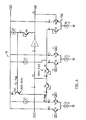
- FIG. 5 shows the operation of the charge pump 18 in the "PUMP DOWN" state.
- the UP input 36 is at logic level 0 and the DOWN input 40 is at logic level 1. Since the logic level on the UP * 36 input is one, transistor Q 2 is turned on and the current sink 1 2 sinks a current 21 (i.e. current source 1 1 supplies I and Q 10 supplies I).
- the zero forward bias condition for diode Q 5 is set up in the same fashion as for the idle condition discussed above.
- the logic level 0 at the DOWN * input 42 keeps transistor Q 4 turned off, hence the current sunk by current sink 1 4 must flow through transistor Q 3 .
- the current source 1 3 supplies half of this quantity, i.e. I, and diode Q 6 sources the remainder, i.e. I to produce current 21. This follows because diode Q 7 cannot source current at its anode.
- the parasitic loading at these nodes must also be essentially the same for both nodes.
- the node at the collector of transistor Q 2 has a tally of 2 collectors (Q 2 and Q 5 ), 1 emitter (Q io ), and 1 current source (1 1 ) which produces a current with magnitude I.
- the tally for the node at the collector of transistor Q 3 is also 2 collectors (Q 3 and Q 7 ), 1 emitter (Q s ) and 1 current source (1 3 ).
- the output current 1 0 is the difference between the currents flowing in diode Q 5 and diode Q 6 , and consequently the output current 1 0 which leaks will not be as low as for the idle state discussed above. However for most applications, this resulting leakage current dos not present a problem.
Landscapes
- Engineering & Computer Science (AREA)
- Microelectronics & Electronic Packaging (AREA)
- Physics & Mathematics (AREA)
- Nonlinear Science (AREA)
- Electromagnetism (AREA)
- General Physics & Mathematics (AREA)
- Radar, Positioning & Navigation (AREA)
- Automation & Control Theory (AREA)
- Power Engineering (AREA)
- Stabilization Of Oscillater, Synchronisation, Frequency Synthesizers (AREA)
- Electrophonic Musical Instruments (AREA)
- Logic Circuits (AREA)
- Superconductors And Manufacturing Methods Therefor (AREA)
- Control Of The Air-Fuel Ratio Of Carburetors (AREA)
Applications Claiming Priority (2)
| Application Number | Priority Date | Filing Date | Title |
|---|---|---|---|
| US08/006,396 US5359299A (en) | 1993-01-21 | 1993-01-21 | High speed and low drift charge pump circuit |
| US6396 | 2001-12-10 |
Publications (3)
| Publication Number | Publication Date |
|---|---|
| EP0608151A2 true EP0608151A2 (de) | 1994-07-27 |
| EP0608151A3 EP0608151A3 (de) | 1995-04-19 |
| EP0608151B1 EP0608151B1 (de) | 2000-05-03 |
Family
ID=21720660
Family Applications (1)
| Application Number | Title | Priority Date | Filing Date |
|---|---|---|---|
| EP94300491A Expired - Lifetime EP0608151B1 (de) | 1993-01-21 | 1994-01-21 | Ladungspumpenschaltung mit hoher Geschwindigkeit und wenig Drift |
Country Status (8)
| Country | Link |
|---|---|
| US (1) | US5359299A (de) |
| EP (1) | EP0608151B1 (de) |
| JP (1) | JP2983823B2 (de) |
| AT (1) | ATE192613T1 (de) |
| CA (1) | CA2113762C (de) |
| DE (1) | DE69424195T2 (de) |
| DK (1) | DK0608151T3 (de) |
| ES (1) | ES2145095T3 (de) |
Cited By (4)
| Publication number | Priority date | Publication date | Assignee | Title |
|---|---|---|---|---|
| GB2312576A (en) * | 1996-04-24 | 1997-10-29 | Motorola Inc | Increasing switching speed of bipolar circuit for charge pump by clamping transistors to prevent saturation |
| US5719845A (en) * | 1995-04-18 | 1998-02-17 | Sony Corporation | Optical pick-up device composed of composite prism made of uniaxial crystal and non-axial crystal |
| WO1998010520A3 (en) * | 1996-09-06 | 1998-05-22 | Philips Electronic N V | Frequency synthesis circuit having a charge pump |
| WO2003069781A3 (en) * | 2002-02-15 | 2004-01-29 | Motorola Inc | Pll arrangement, charge pump, method for charge regulation and mobile transceiver |
Families Citing this family (12)
| Publication number | Priority date | Publication date | Assignee | Title |
|---|---|---|---|---|
| US5619161A (en) * | 1994-08-31 | 1997-04-08 | International Business Machines Corporation | Diffrential charge pump with integrated common mode control |
| US5872733A (en) * | 1995-06-06 | 1999-02-16 | International Business Machines Corporation | Ramp-up rate control circuit for flash memory charge pump |
| US5722052A (en) * | 1996-02-28 | 1998-02-24 | Motorola, Inc. | Switching current mirror for a phase locked loop frequency synthesizer and communication device using same |
| WO2000014922A1 (en) * | 1998-09-03 | 2000-03-16 | Gennum Corporation | Slew phase locked loop |
| ATE300809T1 (de) * | 2000-03-15 | 2005-08-15 | Koninkl Philips Electronics Nv | Leistungsarmer phasen- und frequenzdetektor mit ladungspumpe und ohne totbereich |
| US6819187B1 (en) * | 2002-07-12 | 2004-11-16 | Marvell International Ltd. | Limit swing charge pump and method thereof |
| US7064600B1 (en) | 2002-07-12 | 2006-06-20 | Marvell International Ltd. | Limit swing charge pump and method thereof |
| US7315197B1 (en) | 2002-07-12 | 2008-01-01 | Marvell International Ltd. | Limit swing charge pump and method thereof |
| US7088171B2 (en) * | 2003-06-13 | 2006-08-08 | Texas Instruments Incorporated | Charge pump with constant output current |
| US7535281B2 (en) * | 2006-09-29 | 2009-05-19 | Micron Technology, Inc. | Reduced time constant charge pump and method for charging a capacitive load |
| US7915933B2 (en) | 2006-11-30 | 2011-03-29 | Mosaid Technologies Incorporated | Circuit for clamping current in a charge pump |
| CN101409554B (zh) * | 2007-10-11 | 2012-05-16 | 北京朗波芯微技术有限公司 | 用于电荷泵锁相环的环路滤波电路 |
Family Cites Families (7)
| Publication number | Priority date | Publication date | Assignee | Title |
|---|---|---|---|---|
| US5126692A (en) * | 1987-08-03 | 1992-06-30 | Western Digital Corporation | Variable frequency system having linear combination of charge pump and voltage controlled oscillator |
| JP2879763B2 (ja) * | 1989-06-27 | 1999-04-05 | ソニー株式会社 | Pllのチャージポンプ回路 |
| US4987387A (en) * | 1989-09-08 | 1991-01-22 | Delco Electronics Corporation | Phase locked loop circuit with digital control |
| EP0427084B1 (de) * | 1989-11-08 | 1994-12-14 | National Semiconductor Corporation | Cascodeschaltkreis mit maximalem Hub für eine bipolare Ladungspumpe |
| GB2249443B (en) * | 1990-10-31 | 1994-06-08 | Gen Electric Co Plc | Charge pump circuit |
| JPH04223716A (ja) * | 1990-12-26 | 1992-08-13 | Fujitsu Ltd | Pllシンセサイザ回路 |
| US5095287A (en) * | 1991-01-24 | 1992-03-10 | Motorola, Inc. | Phase locked loop having a charge pump with reset |
-
1993
- 1993-01-21 US US08/006,396 patent/US5359299A/en not_active Expired - Lifetime
-
1994
- 1994-01-19 CA CA002113762A patent/CA2113762C/en not_active Expired - Fee Related
- 1994-01-21 JP JP6005458A patent/JP2983823B2/ja not_active Expired - Fee Related
- 1994-01-21 DE DE69424195T patent/DE69424195T2/de not_active Expired - Fee Related
- 1994-01-21 AT AT94300491T patent/ATE192613T1/de not_active IP Right Cessation
- 1994-01-21 ES ES94300491T patent/ES2145095T3/es not_active Expired - Lifetime
- 1994-01-21 EP EP94300491A patent/EP0608151B1/de not_active Expired - Lifetime
- 1994-01-21 DK DK94300491T patent/DK0608151T3/da active
Cited By (5)
| Publication number | Priority date | Publication date | Assignee | Title |
|---|---|---|---|---|
| US5719845A (en) * | 1995-04-18 | 1998-02-17 | Sony Corporation | Optical pick-up device composed of composite prism made of uniaxial crystal and non-axial crystal |
| GB2312576A (en) * | 1996-04-24 | 1997-10-29 | Motorola Inc | Increasing switching speed of bipolar circuit for charge pump by clamping transistors to prevent saturation |
| GB2312576B (en) * | 1996-04-24 | 2000-06-07 | Motorola Inc | Bipolar switch arrangement |
| WO1998010520A3 (en) * | 1996-09-06 | 1998-05-22 | Philips Electronic N V | Frequency synthesis circuit having a charge pump |
| WO2003069781A3 (en) * | 2002-02-15 | 2004-01-29 | Motorola Inc | Pll arrangement, charge pump, method for charge regulation and mobile transceiver |
Also Published As
| Publication number | Publication date |
|---|---|
| DE69424195T2 (de) | 2000-11-23 |
| EP0608151B1 (de) | 2000-05-03 |
| US5359299A (en) | 1994-10-25 |
| DE69424195D1 (de) | 2000-06-08 |
| EP0608151A3 (de) | 1995-04-19 |
| ES2145095T3 (es) | 2000-07-01 |
| ATE192613T1 (de) | 2000-05-15 |
| DK0608151T3 (da) | 2000-08-07 |
| JP2983823B2 (ja) | 1999-11-29 |
| CA2113762A1 (en) | 1994-07-22 |
| CA2113762C (en) | 1999-12-21 |
| JPH07177026A (ja) | 1995-07-14 |
Similar Documents
| Publication | Publication Date | Title |
|---|---|---|
| US5359299A (en) | High speed and low drift charge pump circuit | |
| US4322643A (en) | Digital phase comparator with improved sensitivity for small phase differences | |
| US4636748A (en) | Charge pump for use in a phase-locked loop | |
| US4091335A (en) | Phase locked loop using current controlled ring oscillator | |
| KR970003096B1 (ko) | 고속 고정 전류 감소 및 클램핑 회로를 구비한 위상 고정 루프 | |
| EP0484059B1 (de) | Lade/Entladeschaltung | |
| US3848139A (en) | High-gain comparator circuit | |
| EP0599517A2 (de) | Bipolare logische Gatter für den Betrieb mit geringen Speisespannungen | |
| US3924202A (en) | Electronic oscillator | |
| EP0427442A2 (de) | Spannungsgesteuerter programmierbarer Ringoszillator | |
| US3010031A (en) | Symmetrical back-clamped transistor switching sircuit | |
| US4714900A (en) | Current output circuit having well-balanced output currents of opposite polarities | |
| US6111469A (en) | Charge pumping circuit and PLL frequency synthesizer | |
| US5357216A (en) | Current sourcing and sinking circuit for driving a VCO charge pump | |
| US3473047A (en) | High speed digital logic circuit having non-saturating output transistor | |
| FI87866C (fi) | Stroemstyrande logisk krets av emitterfoeljartyp | |
| JP3530582B2 (ja) | シングルエンド入力論理ゲートを有する集積論理回路 | |
| US3571616A (en) | Logic circuit | |
| US4695747A (en) | Apparatus increasing diode switching speeds | |
| US4792706A (en) | ECL gates using diode-clamped loads and Schottky clamped reference bias | |
| US4910425A (en) | Input buffer circuit | |
| EP0206816A2 (de) | Vorrichtung zur Beschleunigung der Schaltgeschwindigkeit von Dioden | |
| US5521558A (en) | Inverter stage having diode load and ring oscillator using same | |
| US6384638B1 (en) | Differential charge pump for providing a low charge pump current | |
| US5467051A (en) | Low voltage precision switch |
Legal Events
| Date | Code | Title | Description |
|---|---|---|---|
| PUAI | Public reference made under article 153(3) epc to a published international application that has entered the european phase |
Free format text: ORIGINAL CODE: 0009012 |
|
| AK | Designated contracting states |
Kind code of ref document: A2 Designated state(s): AT BE CH DE DK ES FR GB IE IT LI NL |
|
| PUAL | Search report despatched |
Free format text: ORIGINAL CODE: 0009013 |
|
| AK | Designated contracting states |
Kind code of ref document: A3 Designated state(s): AT BE CH DE DK ES FR GB IE IT LI NL |
|
| RHK1 | Main classification (correction) |
Ipc: H03L 7/089 |
|
| 17P | Request for examination filed |
Effective date: 19951017 |
|
| 17Q | First examination report despatched |
Effective date: 19980323 |
|
| GRAG | Despatch of communication of intention to grant |
Free format text: ORIGINAL CODE: EPIDOS AGRA |
|
| GRAG | Despatch of communication of intention to grant |
Free format text: ORIGINAL CODE: EPIDOS AGRA |
|
| GRAH | Despatch of communication of intention to grant a patent |
Free format text: ORIGINAL CODE: EPIDOS IGRA |
|
| GRAH | Despatch of communication of intention to grant a patent |
Free format text: ORIGINAL CODE: EPIDOS IGRA |
|
| GRAA | (expected) grant |
Free format text: ORIGINAL CODE: 0009210 |
|
| AK | Designated contracting states |
Kind code of ref document: B1 Designated state(s): AT BE CH DE DK ES FR GB IE IT LI NL |
|
| REF | Corresponds to: |
Ref document number: 192613 Country of ref document: AT Date of ref document: 20000515 Kind code of ref document: T |
|
| REG | Reference to a national code |
Ref country code: CH Ref legal event code: NV Representative=s name: ISLER & PEDRAZZINI AG Ref country code: CH Ref legal event code: EP |
|
| REG | Reference to a national code |
Ref country code: IE Ref legal event code: FG4D |
|
| ITF | It: translation for a ep patent filed | ||
| REF | Corresponds to: |
Ref document number: 69424195 Country of ref document: DE Date of ref document: 20000608 |
|
| REG | Reference to a national code |
Ref country code: ES Ref legal event code: FG2A Ref document number: 2145095 Country of ref document: ES Kind code of ref document: T3 |
|
| ET | Fr: translation filed | ||
| REG | Reference to a national code |
Ref country code: DK Ref legal event code: T3 |
|
| PG25 | Lapsed in a contracting state [announced via postgrant information from national office to epo] |
Ref country code: AT Free format text: LAPSE BECAUSE OF NON-PAYMENT OF DUE FEES Effective date: 20010121 |
|
| PG25 | Lapsed in a contracting state [announced via postgrant information from national office to epo] |
Ref country code: IE Free format text: LAPSE BECAUSE OF NON-PAYMENT OF DUE FEES Effective date: 20010122 Ref country code: ES Free format text: LAPSE BECAUSE OF NON-PAYMENT OF DUE FEES Effective date: 20010122 |
|
| PG25 | Lapsed in a contracting state [announced via postgrant information from national office to epo] |
Ref country code: LI Free format text: LAPSE BECAUSE OF NON-PAYMENT OF DUE FEES Effective date: 20010131 Ref country code: CH Free format text: LAPSE BECAUSE OF NON-PAYMENT OF DUE FEES Effective date: 20010131 Ref country code: BE Free format text: LAPSE BECAUSE OF NON-PAYMENT OF DUE FEES Effective date: 20010131 |
|
| PLBE | No opposition filed within time limit |
Free format text: ORIGINAL CODE: 0009261 |
|
| STAA | Information on the status of an ep patent application or granted ep patent |
Free format text: STATUS: NO OPPOSITION FILED WITHIN TIME LIMIT |
|
| 26N | No opposition filed | ||
| BERE | Be: lapsed |
Owner name: GENNUM CORP. Effective date: 20010131 |
|
| REG | Reference to a national code |
Ref country code: CH Ref legal event code: PL |
|
| REG | Reference to a national code |
Ref country code: IE Ref legal event code: MM4A |
|
| REG | Reference to a national code |
Ref country code: GB Ref legal event code: IF02 |
|
| REG | Reference to a national code |
Ref country code: ES Ref legal event code: FD2A Effective date: 20020211 |
|
| PGFP | Annual fee paid to national office [announced via postgrant information from national office to epo] |
Ref country code: DK Payment date: 20050126 Year of fee payment: 12 Ref country code: DE Payment date: 20050126 Year of fee payment: 12 |
|
| PGFP | Annual fee paid to national office [announced via postgrant information from national office to epo] |
Ref country code: FR Payment date: 20050127 Year of fee payment: 12 |
|
| PGFP | Annual fee paid to national office [announced via postgrant information from national office to epo] |
Ref country code: NL Payment date: 20050131 Year of fee payment: 12 |
|
| PGFP | Annual fee paid to national office [announced via postgrant information from national office to epo] |
Ref country code: GB Payment date: 20060125 Year of fee payment: 13 |
|
| PG25 | Lapsed in a contracting state [announced via postgrant information from national office to epo] |
Ref country code: FR Free format text: LAPSE BECAUSE OF NON-PAYMENT OF DUE FEES Effective date: 20060131 Ref country code: DK Free format text: LAPSE BECAUSE OF NON-PAYMENT OF DUE FEES Effective date: 20060131 |
|
| PGFP | Annual fee paid to national office [announced via postgrant information from national office to epo] |
Ref country code: IT Payment date: 20060131 Year of fee payment: 13 |
|
| PG25 | Lapsed in a contracting state [announced via postgrant information from national office to epo] |
Ref country code: NL Free format text: LAPSE BECAUSE OF NON-PAYMENT OF DUE FEES Effective date: 20060801 Ref country code: DE Free format text: LAPSE BECAUSE OF NON-PAYMENT OF DUE FEES Effective date: 20060801 |
|
| REG | Reference to a national code |
Ref country code: DK Ref legal event code: EBP |
|
| NLV4 | Nl: lapsed or anulled due to non-payment of the annual fee |
Effective date: 20060801 |
|
| REG | Reference to a national code |
Ref country code: FR Ref legal event code: ST Effective date: 20060929 |
|
| GBPC | Gb: european patent ceased through non-payment of renewal fee |
Effective date: 20070121 |
|
| PG25 | Lapsed in a contracting state [announced via postgrant information from national office to epo] |
Ref country code: GB Free format text: LAPSE BECAUSE OF NON-PAYMENT OF DUE FEES Effective date: 20070121 |
|
| PG25 | Lapsed in a contracting state [announced via postgrant information from national office to epo] |
Ref country code: IT Free format text: LAPSE BECAUSE OF NON-PAYMENT OF DUE FEES Effective date: 20070121 |