EP0608875A1 - Anlage zum Ziehen eines Einkristalls und Verfahren zum Entfernen von Siliziumoxid - Google Patents
Anlage zum Ziehen eines Einkristalls und Verfahren zum Entfernen von Siliziumoxid Download PDFInfo
- Publication number
- EP0608875A1 EP0608875A1 EP94101192A EP94101192A EP0608875A1 EP 0608875 A1 EP0608875 A1 EP 0608875A1 EP 94101192 A EP94101192 A EP 94101192A EP 94101192 A EP94101192 A EP 94101192A EP 0608875 A1 EP0608875 A1 EP 0608875A1
- Authority
- EP
- European Patent Office
- Prior art keywords
- monocrystal
- carrier gas
- gap
- pulling
- flow path
- Prior art date
- Legal status (The legal status is an assumption and is not a legal conclusion. Google has not performed a legal analysis and makes no representation as to the accuracy of the status listed.)
- Granted
Links
- VYPSYNLAJGMNEJ-UHFFFAOYSA-N Silicium dioxide Chemical compound O=[Si]=O VYPSYNLAJGMNEJ-UHFFFAOYSA-N 0.000 title claims abstract description 83
- 229910052814 silicon oxide Inorganic materials 0.000 title claims abstract description 62
- 238000000034 method Methods 0.000 title claims abstract description 28
- 239000012159 carrier gas Substances 0.000 claims abstract description 120
- 239000000155 melt Substances 0.000 claims abstract description 76
- XUIMIQQOPSSXEZ-UHFFFAOYSA-N Silicon Chemical compound [Si] XUIMIQQOPSSXEZ-UHFFFAOYSA-N 0.000 claims abstract description 24
- 229910052710 silicon Inorganic materials 0.000 claims abstract description 24
- 239000010703 silicon Substances 0.000 claims abstract description 24
- 230000008016 vaporization Effects 0.000 claims abstract description 18
- 239000000463 material Substances 0.000 claims abstract description 8
- QVGXLLKOCUKJST-UHFFFAOYSA-N atomic oxygen Chemical compound [O] QVGXLLKOCUKJST-UHFFFAOYSA-N 0.000 claims description 68
- 229910052760 oxygen Inorganic materials 0.000 claims description 68
- 239000001301 oxygen Substances 0.000 claims description 68
- OKTJSMMVPCPJKN-UHFFFAOYSA-N Carbon Chemical compound [C] OKTJSMMVPCPJKN-UHFFFAOYSA-N 0.000 claims description 27
- 229910052799 carbon Inorganic materials 0.000 claims description 19
- 238000001816 cooling Methods 0.000 claims description 15
- 238000010438 heat treatment Methods 0.000 claims description 14
- HBMJWWWQQXIZIP-UHFFFAOYSA-N silicon carbide Chemical compound [Si+]#[C-] HBMJWWWQQXIZIP-UHFFFAOYSA-N 0.000 claims description 4
- 229910010271 silicon carbide Inorganic materials 0.000 claims description 3
- 239000013078 crystal Substances 0.000 description 42
- 239000010453 quartz Substances 0.000 description 21
- 238000009826 distribution Methods 0.000 description 16
- 230000000694 effects Effects 0.000 description 15
- 239000007789 gas Substances 0.000 description 12
- 238000009834 vaporization Methods 0.000 description 12
- 238000005094 computer simulation Methods 0.000 description 10
- 238000013459 approach Methods 0.000 description 9
- 238000004458 analytical method Methods 0.000 description 8
- 229910002804 graphite Inorganic materials 0.000 description 8
- 239000010439 graphite Substances 0.000 description 8
- XKRFYHLGVUSROY-UHFFFAOYSA-N Argon Chemical compound [Ar] XKRFYHLGVUSROY-UHFFFAOYSA-N 0.000 description 6
- 230000008859 change Effects 0.000 description 4
- 238000000151 deposition Methods 0.000 description 4
- 238000009792 diffusion process Methods 0.000 description 4
- 238000004519 manufacturing process Methods 0.000 description 4
- 230000002093 peripheral effect Effects 0.000 description 4
- 229910052786 argon Inorganic materials 0.000 description 3
- 230000002829 reductive effect Effects 0.000 description 3
- 230000000630 rising effect Effects 0.000 description 3
- ZOKXTWBITQBERF-UHFFFAOYSA-N Molybdenum Chemical compound [Mo] ZOKXTWBITQBERF-UHFFFAOYSA-N 0.000 description 2
- 230000002411 adverse Effects 0.000 description 2
- 230000015572 biosynthetic process Effects 0.000 description 2
- 230000000903 blocking effect Effects 0.000 description 2
- 238000010276 construction Methods 0.000 description 2
- 230000007423 decrease Effects 0.000 description 2
- 230000008021 deposition Effects 0.000 description 2
- 239000002019 doping agent Substances 0.000 description 2
- 239000012530 fluid Substances 0.000 description 2
- 229910001385 heavy metal Inorganic materials 0.000 description 2
- 229910052750 molybdenum Inorganic materials 0.000 description 2
- 239000011733 molybdenum Substances 0.000 description 2
- 239000002245 particle Substances 0.000 description 2
- 238000005192 partition Methods 0.000 description 2
- 229910021420 polycrystalline silicon Inorganic materials 0.000 description 2
- 238000001953 recrystallisation Methods 0.000 description 2
- 239000003870 refractory metal Substances 0.000 description 2
- LIVNPJMFVYWSIS-UHFFFAOYSA-N silicon monoxide Chemical compound [Si-]#[O+] LIVNPJMFVYWSIS-UHFFFAOYSA-N 0.000 description 2
- XLYOFNOQVPJJNP-UHFFFAOYSA-N water Substances O XLYOFNOQVPJJNP-UHFFFAOYSA-N 0.000 description 2
- GXCLVBGFBYZDAG-UHFFFAOYSA-N N-[2-(1H-indol-3-yl)ethyl]-N-methylprop-2-en-1-amine Chemical compound CN(CCC1=CNC2=C1C=CC=C2)CC=C GXCLVBGFBYZDAG-UHFFFAOYSA-N 0.000 description 1
- 229910052787 antimony Inorganic materials 0.000 description 1
- 229910052785 arsenic Inorganic materials 0.000 description 1
- 229910052796 boron Inorganic materials 0.000 description 1
- 239000011248 coating agent Substances 0.000 description 1
- 238000000576 coating method Methods 0.000 description 1
- 230000000052 comparative effect Effects 0.000 description 1
- 238000009833 condensation Methods 0.000 description 1
- 230000005494 condensation Effects 0.000 description 1
- 238000013461 design Methods 0.000 description 1
- 230000001627 detrimental effect Effects 0.000 description 1
- -1 for example Substances 0.000 description 1
- 238000005247 gettering Methods 0.000 description 1
- 230000002401 inhibitory effect Effects 0.000 description 1
- 239000007788 liquid Substances 0.000 description 1
- 238000005259 measurement Methods 0.000 description 1
- 230000008018 melting Effects 0.000 description 1
- 238000002844 melting Methods 0.000 description 1
- 238000012986 modification Methods 0.000 description 1
- 230000004048 modification Effects 0.000 description 1
- 230000036961 partial effect Effects 0.000 description 1
- 229910052698 phosphorus Inorganic materials 0.000 description 1
- 238000001556 precipitation Methods 0.000 description 1
- 230000008569 process Effects 0.000 description 1
- 230000009467 reduction Effects 0.000 description 1
- 230000004044 response Effects 0.000 description 1
- XUIMIQQOPSSXEZ-RNFDNDRNSA-N silicon-32 atom Chemical compound [32Si] XUIMIQQOPSSXEZ-RNFDNDRNSA-N 0.000 description 1
- 238000004088 simulation Methods 0.000 description 1
- 238000005507 spraying Methods 0.000 description 1
- 229910052717 sulfur Inorganic materials 0.000 description 1
- 229910052721 tungsten Inorganic materials 0.000 description 1
- WFKWXMTUELFFGS-UHFFFAOYSA-N tungsten Chemical compound [W] WFKWXMTUELFFGS-UHFFFAOYSA-N 0.000 description 1
- 239000010937 tungsten Substances 0.000 description 1
- 238000009827 uniform distribution Methods 0.000 description 1
Images


Classifications
-
- C—CHEMISTRY; METALLURGY
- C30—CRYSTAL GROWTH
- C30B—SINGLE-CRYSTAL GROWTH; UNIDIRECTIONAL SOLIDIFICATION OF EUTECTIC MATERIAL OR UNIDIRECTIONAL DEMIXING OF EUTECTOID MATERIAL; REFINING BY ZONE-MELTING OF MATERIAL; PRODUCTION OF A HOMOGENEOUS POLYCRYSTALLINE MATERIAL WITH DEFINED STRUCTURE; SINGLE CRYSTALS OR HOMOGENEOUS POLYCRYSTALLINE MATERIAL WITH DEFINED STRUCTURE; AFTER-TREATMENT OF SINGLE CRYSTALS OR A HOMOGENEOUS POLYCRYSTALLINE MATERIAL WITH DEFINED STRUCTURE; APPARATUS THEREFOR
- C30B29/00—Single crystals or homogeneous polycrystalline material with defined structure characterised by the material or by their shape
- C30B29/02—Elements
- C30B29/06—Silicon
-
- C—CHEMISTRY; METALLURGY
- C30—CRYSTAL GROWTH
- C30B—SINGLE-CRYSTAL GROWTH; UNIDIRECTIONAL SOLIDIFICATION OF EUTECTIC MATERIAL OR UNIDIRECTIONAL DEMIXING OF EUTECTOID MATERIAL; REFINING BY ZONE-MELTING OF MATERIAL; PRODUCTION OF A HOMOGENEOUS POLYCRYSTALLINE MATERIAL WITH DEFINED STRUCTURE; SINGLE CRYSTALS OR HOMOGENEOUS POLYCRYSTALLINE MATERIAL WITH DEFINED STRUCTURE; AFTER-TREATMENT OF SINGLE CRYSTALS OR A HOMOGENEOUS POLYCRYSTALLINE MATERIAL WITH DEFINED STRUCTURE; APPARATUS THEREFOR
- C30B15/00—Single-crystal growth by pulling from a melt, e.g. Czochralski method
-
- Y—GENERAL TAGGING OF NEW TECHNOLOGICAL DEVELOPMENTS; GENERAL TAGGING OF CROSS-SECTIONAL TECHNOLOGIES SPANNING OVER SEVERAL SECTIONS OF THE IPC; TECHNICAL SUBJECTS COVERED BY FORMER USPC CROSS-REFERENCE ART COLLECTIONS [XRACs] AND DIGESTS
- Y10—TECHNICAL SUBJECTS COVERED BY FORMER USPC
- Y10T—TECHNICAL SUBJECTS COVERED BY FORMER US CLASSIFICATION
- Y10T117/00—Single-crystal, oriented-crystal, and epitaxy growth processes; non-coating apparatus therefor
- Y10T117/10—Apparatus
- Y10T117/1024—Apparatus for crystallization from liquid or supercritical state
- Y10T117/1032—Seed pulling
- Y10T117/1068—Seed pulling including heating or cooling details [e.g., shield configuration]
-
- Y—GENERAL TAGGING OF NEW TECHNOLOGICAL DEVELOPMENTS; GENERAL TAGGING OF CROSS-SECTIONAL TECHNOLOGIES SPANNING OVER SEVERAL SECTIONS OF THE IPC; TECHNICAL SUBJECTS COVERED BY FORMER USPC CROSS-REFERENCE ART COLLECTIONS [XRACs] AND DIGESTS
- Y10—TECHNICAL SUBJECTS COVERED BY FORMER USPC
- Y10T—TECHNICAL SUBJECTS COVERED BY FORMER US CLASSIFICATION
- Y10T117/00—Single-crystal, oriented-crystal, and epitaxy growth processes; non-coating apparatus therefor
- Y10T117/10—Apparatus
- Y10T117/1024—Apparatus for crystallization from liquid or supercritical state
- Y10T117/1032—Seed pulling
- Y10T117/1072—Seed pulling including details of means providing product movement [e.g., shaft guides, servo means]
Definitions
- the present invention relates to a monocrystal pulling-up system which pulls up and grows a monocrystal of silicon etc. by the Czochralski technique (hereinafter referred to as the "CZ technique"), in particular relates to a monocrystal pulling-up system which can pull a large diameter and high quality monocrystal while controlling the oxygen concentration (density) by providing a carrier gas flow controller.
- CZ technique Czochralski technique
- the present invention also relates to a method of exhausting silicon oxide(SiO) produced from the melt silicon in a quartz crucible to the outside of a pulling chamber by controlling the flow of the carrier gas.
- polycrystalline silicon and the necessary dopant(s), for example, P, B, Sb, As are inserted into a quartz crucible provided rotatably at a bottom of a pulling chamber, the chamber is evacuated to a vacuum, then a heater arranged around the quarts crucible is used to melt the polycrystalline silicon and the dopant(s).
- a carrier gas is then passed from an upper portion of the chamber to the quartz crucible.
- a seed crystal (starting crystal) attached to and supported by a chuck on a pulling shaft is immersed in the melt silicon in the quartz crucible under conditions of a vacuum of 10 to 20 Torr. Then the pulling shaft is pulled up at a predetermined speed while relatively rotating it with respect to the quartz crucible.
- U.S. Patent No. 4,330,362 discloses a pulling system provided with a member (hereinafter called a "heat cap") comprised of a material able to reflect ultraviolet rays above the crucible so as to partially cover the crucible and the melt silicon in the crucible, to thereby block the radiant heat from the melt surface, promote the formation of the monocrystal, and raise the pulling speed and to keep down the concentration of carbon in the monocrystal.
- the above heat cap can be expected to a certain extent to have the effect of controlling the flow of the carrier gas, for example, argon gas(Ar), being passed to remove the silicon oxide(SiO) produced from the melt and efficiently eliminating the silicon oxide depositing on the inner wall of the top end of the crucible, but silicon oxide ends up depositing and condensing on the top of the heat cap itself.
- the carrier gas for example, argon gas(Ar)
- the heat cap has as its main object the literal blocking of ultraviolet rays and is not designed with the intention of control of the flow of the argon gas.
- the melt surface near the inner peripheral wall of the quarts crucible ends up being covered by the heat cap, so an operator cannot visually inspect the melt surface from a peephole etc. provided in the pulling chamber.
- the disadvantage that it is not possible to quickly deal with any heat deformation of the top end of the crucible, recrystallization or deposition of silicon near the inner peripheral wall of the crucible, or any other disadvantages when they occurred.
- the "oxygen in the crystal” described here means the oxygen dissolving out from the quartz crucible. Almost of the oxygen, for example, 95 % of the oxygen, becomes silicon oxide and is exhausted by the carrier gas to the outside of the pulling chamber. Therefore, the following techniques ore known for the control of the oxygen concentration in the crystal: Approach (1): Changing the rotational speed of the crucible go as to control the supply of oxygen from the wall of the quartz crucible. By this technique, if the rotational speed of the crucible is increased, the amount of oxygen of the pulled monocrystal becomes higher. However, if the rotational speed of the crucible is made lower, the temperature fluctuations of the melt become great and crystal faults become easier to occur at a low oxygen concentration.
- Approach (3) Spraying carrier gas on the melt silicon surface in the crucible so as to control the temperature of the melt silicon surface and control the amount of vaporization of the silicon oxide.
- the carrier gap between the heat cap and the melt silicon surface and the gap between the heat cap and the pulled monocrystal (hereinafter referred to all together as the "bottom gap") are controlled.
- the bottom gap is made smaller, the temperature of the melt surface falls, so the amount of vaporization of the silicon oxide is held down and as a result the amount of oxygen of the pulled monocrystal becomes higher.
- Approach (4) Control of the discharge of the vaporized silicon oxide by the flow of the carrier gas. If the vaporized silicon oxide is efficiently discharged by the carrier gas from the melt silicon surface to outside of the pulling chamber, the vaporization of the silicon oxide is promoted and as a result the oxygen concentration in the melt is lowered and the amount of oxygen in the pulled crystal becomes lower. There is a gas diffusion layer of the vaporized silicon oxide directly above the melt surface. By using the heat cap, the flow rate of the same is increased by the flow of the carrier gas introduced from above the pulling chamber in the narrowed gap between the heat cap and the melt surface and therefore the thickness of the gas diffusion layer is reduced.
- the partial pressure of the silicon oxide on the melt surface becomes lower and vaporization of the silicon oxide is promoted, but if a heat cap is used, an opposing phenomenon simultaneously occurs. Further, if the crucible deforms and the melt surface drops, the subsequent oxygen concentration in the crystal will change.
- Japanese Unexamined Patent Publication (Kokai) No. 3-275586 discloses the production of a crystal with a high oxide film pressure resistance by lowering the pulling speed to 0.5 mm/min or less in a furnace structure with a usual pulling speed of 1.5 mm/min. This is because it is guessed that by lengthening the residence time in the temperature region of over 1300°C from the crystal growth interface, the faults relating to the pressure resistance of the oxide film diffuse and disappear.
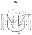
- Figure 1 is a view showing the state of flow of carrier gas in a pulling system equipped with a closed type heat cap
- Fig. 2 is a view of the state of flow of carrier gas analyzed by computer simulation of the Navier-Stokes equation
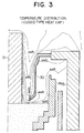
- Fig. 3 is a view of the temperature distribution obtained by analysis by the same computer simulation.
- the heat cap 30 shown in Fig. 1 completely partitions the flow path of the carrier gas G into the top (shown by region X) and bottom (shown by region Y) of a pulling chamber, so the carrier gas G introduced from the top of the pulling chamber passes through the narrow bottom gap 33 between the heat cap 30 and the pulled monocrystal 31 and surface of the melt silicon 32 to be increased in speed.
- the carrier gas forcibly removes the diffusion layer including the silicon oxide from the melt surface, so vaporization of silicon oxide is promoted.
- the degree of contact with the carrier gas G is smaller than with the portion 34 directly under the bottom gap 33, so the melt becomes relatively low in oxygen concentration. Therefore, the distribution of the oxygen concentration of the melt in the crucible becomes nonuniform and there is an adverse effect on the oxygen distribution (ORG) in the silicon wafer surface of the pulled monocrystal 31.
- a heat-cap disclosed in JPP 1-100,086 comprises a reflector body and projected stops.
- the reflector consists of a tube and an inclined cylinder provided at a lower portion of the tube with a tip (end) which is reduced in diameter inward.
- the tube and the inclined cylinder may be formed integrally or together.
- Projections are provided at the top of the tube and are affixed to the top of a heat retaining member provided around the crucible.
- the carrier gas is branched by the tube to flow, on one hand, through a gap between the pulling monocrystal and the tube, and, other hand, through a gap between the tube and the heat retaining member. That is, the heat cap can form a flow path between the tube and the heat holding member.
- the heat cap can be called an open-type heat cap.
- JPP 1-100,086 can overcome the disadvantage of U.S. Patent No. 4,330,362 as a basic idea, but JPP 1-100,086 does not disclose specific conditions. In addition, the heat cap of JPP 1-100,086 requires some improvements.
- An object of the present invention is to provide a pulling system which enables control of the oxygen concentration of the pulled monocrystal, can make the oxygen concentration (ORG) in a wafer surface uniform, can pull a monocrystal with a uniform oxygen concentration in the axial direction, and in particular can pull a large diameter monocrystal with a high quality and a uniform heat history.
- Another object of the present invention is to provide a method of exhausting silicon oxide by a carrier gas effectively and a system thereof.
- Still another object of the present invention is to provide an improved heat cap.
- a monocrystal pulling system comprising: a pulling chamber; a crucible provided inside the pulling chamber; a heating means provided at the circumference of the crucible and for melting a material accommodated in the crucible for forming the monocrystal; a heat retention means provided a predetermined distance away from the heating means and for retaining the heat of the crucible; a means for supplying a carrier gas from the top of the pulling chamber toward the surface of the melt solution in the crucible; and a flow controller which guides the carrier gas to the surface of the melt of the material forming the monocrystal and exhausts the silicon oxide vaporizing from the surface of the melt solution to the outside of the pulling chamber and which surrounds the pulled monocrystal near the surface of the melt and is provided partially inside the crucible.
- the flow controller comprises a tubular portion which has an outer diameter smaller than the inner diameter of the crucible and extends substantially perpendicularly along the direction of downward flow of the carrier gas, a constricted diameter portion which constricts in diameter from the bottom end of the tubular portion and forms a bottom gap with the pulled monocrystal, and an engagement portion which projects out from the top of the tubular portion and forms a top gap at the outer circumference of the tubular portion of said flow controller by supporting the flow controller partially in the pulling chamber.
- a first flow path through which the carrier gas flows toward the bottom gap is defined between the inside of the tubular portion and the pulled up monocrystal
- a second flow path is defined comprised of a flow path of the carrier gas passing through the top gap and a flow path of the carrier gas passing from the first flow path through the bottom gap and then passing between the surface of the silicon melt solution and the flow controller.
- the silicon oxide is exhausted together with the carrier gas through the second flow path to the outside of the pulling chamber.
- the bottom gap and the top gap are formed so that the amount of the carrier gas flowing through the bottom gap becomes greater than the amount of the carrier gas flowing through the top gap.
- the engagement portion is affixed to the top of a heat retaining tube provided at the outer circumference of the crucible.
- a heating means for heating the crucible is arranged between the crucible and the heat retaining tuba, a gap is formed between the heating means and the heat retaining tube, the gap is connected to the second flow path, and the silicon oxide is exhausted together with the carrier gas to the outside of the pulling chamber through the gap.
- the area of the opening of the constricted diameter portion is 1.5 to 2.0 times the sectional area of the pulled monocrystal.
- the sectional area (Ru) of the top gap is 0.5 to 1.4 times the sectional area (Rd) of the bottom gap.
- the top gap is positioned at least partially to the inside of the top end of the crucible.
- the flow controller is made of carbon.
- the surface of said carbon flow controller is covered with silicon carbide.
- the length of the tubular portion of said flow controller is greater than the range of vertical movement of said crucible.
- the tubular portion, the constricted diameter portion, and the engagement portion are integrally formed, or, the tubular portion and the constricted diameter portion are integrally formed and the engagement portion is attached detachably to the tubular portion.
- a silicon oxide exhaust method for guiding a carrier gas, supplied from the top of a pulling chamber for pulling up a monocrystal according to the Czochralski technique, to a surface of a melt of a material for forming a monocrystal and exhausting to the outside of the pulling chamber a silicon oxide vaporized from the surface of the melt accommodated in a crucible.
- the silicon oxide exhaust method characterized by defining by a carrier gas branching moans a bottom gap of a predetermined size between a circumference of the pulled monocrystal and the surface of the melt and defining a top gap between the crucible and a heat retaining tube provided at the outside of the same, defining a first flow path through which the carrier gas flows toward the bottom gap between the carrier gas branching means and pulled monocrystal, defining a second flow path comprised of a flow path of the carrier gas passing through the top gap and a flow path of said carrier gas passing from the first flow path through the bottom gap and then passing between the surface of the silicon melt and a flow controller, forming the bottom gap and the top gap so that the amount of the carrier gas flowing through the bottom gap becomes greater than the amount of the carrier gas flowing through the top gap, and exhausting said silicon oxide together with said carrier gas through said second flow path to the outside of the pulling chamber.
- the crucible is heated by a heating means arranged between the crucible and the heat retaining tube and a gap is formed between the heating means and the heat retaining tube, the gap is connected to the second flow path, and the silicon oxide is exhausted together with the carrier gas to the outside of said pulling chamber through the gap.
- the diameter of the carrier gas branching means near the surface of the melt solution is constricted and the area of the opening of the constricted diameter portion is 1.5 to 2.0 times the sectional area of the pulled monocrystal.
- the sectional area (Ru) of said top gap is 0.5 to 1.4 times the sectional area (Rd) of the bottom gap.
- the top gap is positioned at least partially to the inside of the top end of the crucible.
- a monocrystal pulling system further provision is made of a rotational control means for controlling the relative rotational speed of the crucible or the pulled monocrystal so as to control the concentration of oxygen included in the monocrystal.
- a monocrystal pulling method wherein the relative rotational speed of the crucible or the pulled monocrystal is controlled so as to control the concentration of oxygen included in the monocrystal.
- the silicon oxide which condenses at the top of the pulling apparatus and at the crystal surface and falls into the melt becomes a cause of ruin of the monocrystal, so it is critical to exhaust the vaporized silicon oxide by the carrier gas out of the system quickly and smoothly.
- the optimal flow of carrier gas is realized, the amount of vaporization of the silicon oxide is made constant, and the particles of the silicon oxide pass between a graphite susceptor and heat shield and between the heat shield and heater and are exhausted by a vacuum pump without condensing and solidifying.
- the carrier gas does not flow in a squished manner as in the conventional pulling apparatus. Rather, the aspiration effect of the carrier gas passing through the second flow path formed at the outer portion of the flow controller is utilized and the carrier gas that passes through the inside of the flow controller and sweeps up and exhausts the atmosphere including the silicon oxide particles from the melt surface is used to draw this to the outer portion of the crucible.
- the carrier gas flowing down along the inner portion of the flow controller (first flow path) is heated by the carbon flow controller, passes through the gap, then is led to the melt surface without excessively cooling the melt, and promotes the vaporization of the silicon oxide.
- the atmosphere including the silicon oxide is led uniformly outside by the aspiration effect of the large energy carrier gas passing through the outer portion of the flow controller (second flow path).
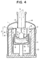
- the pulling system of the present embodiment provides a quartz crucible 3 in a pulling chamber 1.
- the quartz crucible 3 is attached to a rotatable bottom shaft 9 through a graphite susceptor 8. Further, around the quartz crucible 3 is provided a heater 10 for heating and controlling the temperature of the silicon melt M in the quartz crucible 3. Between the heater 10 and the pulling chamber 1 is provided a heat retaining tube 11.
- an annular supporting member 12 At the top surface of the heat retaining tube 11 is attached an annular supporting member 12. By placing an engagement portion 7 of a flow controller 2 on the supporting member 12, the flow controller 2 is affixed inside the pulling chamber.
- reference numeral 13 denotes a cooling tube for cooling the pulled monocrystal
- reference numeral 14 denotes a peephole for observing the surface of the melt M and the top end edge of the quartz crucible 3.
- the flow controller 2 has an outer diameter d smaller than the inner diameter D of the quartz crucible 3 and is comprised of a tubular portion 4 which extends substantially perpendicularly along the direction of downward flow of the carrier gas G and a constricted diameter portion 6 which constricts in diameter gradually from the bottom end of the tubular portion 4 and forms the small bottom gap 5 with the pulled monocrystal S.
- the tubular portion 4 is particularly effective in the case of pulling the monocrystal by the batch-type CZ technique.
- the height of the tubular portion 4 in the present embodiment is set so that the area of the opening of the opening 17 becomes constant even if the graphite susceptor 8 is moved up and down between the limit of descent and the limit of rise. Therefore, even if the graphite susceptor 8 rises along with the pulling of the monocrystal, the area of the opening 17 can be held constant, so there is no fluctuation in the flow of the carrier gas G mentioned later.
- the above numerical figures limit the ratio between the area of the opening at the front end of the constricted diameter portion and the lateral sectional area of the monocrystal, but in the flow controller according to the present invention, the same effect is obtained even if the ratio between the area of the bottom gap and the lateral sectional area of the monocrystal is limited.
- the ratio in this case is 0.5 to 1.0.
- the flow controller 2 must withstand high temperatures and not discharge any heavy metal elements since it is directly above the melt.
- a refractory metal like molybdenum(Mo) or tungsten(W) or carbon(C).
- Mo molybdenum
- W tungsten
- C carbon
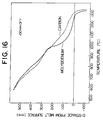
- Figure 16 is a graph showing the results of measurement of the temperature for comparing the effects of radiant heat of molybednum and carbon at a position 100 mm off from the center of the pulling system.
- a carbon flow controller As shown by this temperature distribution, if use is made of a carbon flow controller, the temperature at the crystal growth interface becomes high, so in the past it was considered that this was detrimental to increasing the pulling speed, but since the crystal quality is considered important now, use of carbon is effective.
- a carbon flow controller has the effect of heating the carrier gas flowing through the first flow path P1.
- the surface of the carbon flow controller be coated with silicon carbide(SiC). Giving this silicon carbide coating is advantageous to the lifetime of the flow controller 2 and, further, is effective in inhibiting the discharge of the heavy metal elements included in small amounts in the carbon.
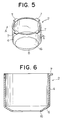
- the engagement portion 7 for placing the flow controller 2 on the supporting member 12 may be formed integrally with the tubular portion 4 as shown in Fig. 5 and Fig. 6. Further, as shown in Fig. 7 and Fig. 8, the engagement portion 7 may be formed separately and be affixed to the tubular portion 4 by carbon bolts 15.
- the flow paths of the carrier gas G supplied from the top of the pulling chamber 1 become as follows: As shown in Fig. 10, first, as the first flow path, there is the flow path P1 in which the carrier gas G branches at the top end of the tubular portion 4 of the flow controller 2 and reaches the inside of the tubular portion 4.
- the carrier gas G passes from the first flow path P1 through the gap between the bottom end of the constricted diameter portion 6 and the pulled monocrystal S (hereinafter referred to as the "bottom gap 5") and through the gap between the bottom end of the constricted diameter portion 6 and the surface of the melt M, then passes between the surface of the melt M and the flow controller 2, and further forms the atmosphere including the silicon oxide accompanying the rising air flow between the flow controller 2 and the inner surface 3a of the quartz crucible.
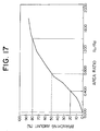
- the ratio of the carrier gas G led through the first flow path P1 and the second flow path P2 is related to the areas of the top and bottom gaps, that is, the area Ru of the gap at the outer portion of the tubular portion of the flow controller 2 in the second flow path P2 (hereinafter this gap is referred to as the "top gap 18") and the area Rd of the bottom gap 5 between the constricted diameter portion 6 of the flow controller 2 and the pulled monocrystal S in the first flow path P1, but the carrier gas flowing through the bottom gap 5 encounters the resistance of the rising air flow from the melt, so judging from the results of simulation of the embodiments shown in Fig. 11 and Fig. 13, when the area ratio Ru/Rd is about 0.7, the carrier gas G flows in equal amounts (branching ratio 50%) in the first flow path P1 and the second flow path P2.
- the carrier gas flowing through the first flow path P1 preferably should be 20% to 80% of the total amount. Converting this to the area ratio Ru/Rd between the top gap 18 and the bottom gap 5, the preferable region of the ratio may be said to be 0.4 to 1.4 (see Fig. 17).
- the carrier gas G led into the second flow path P2 is heated by the carbon flow controller 2 and strikes the melt surface M without overcooling the crystal growth interface, replaces the atmosphere including the silicon oxide removed by the carrier gas from the first flow path P1, and diffuses over the melt surface as a whole. This determines the amount of vaporization of the silicon oxide, defines the oxygen concentration of the melt surface from which the crystal is raised, and stabilizes it at the low oxygen side.
- the second flow path P2 there is the flow path in which the carrier gas G supplied from the top of the pulling chamber 1 branches at the top end of the tubular portion 4 of the flow controller 2 and passes through the top gap 18 to flow to the outer portion of the tubular portion 4.
- the carrier gas G led to this second flow path P2 ends up working with the carrier gas G passing through the first flow path P1 and the other second flow path P2 to function to exhaust the silicon oxide outside the system and, further, has the following functions:
- the carrier gas G branching at the top end of the tubular portion 4 of the flow controller 2 and passing through the top gap 18 to be led into the second flow path P2 flows down along the outer surface of the flow controller 2 and then flows further down along the outer surface of the graphite susceptor 8, that is, when passing through the opening 18 between the graphite susceptor 8 and the flow controller 2, it sweeps up the atmosphere including the silicon oxide at the outside of the flow controller 2 by the aspiration effect and reduces the air pressure.
- the silicon oxide vaporizing from the surface of the melt M is exhausted outside of the quartz crucible 3 along with the large energy gas from the flow path P1, so will not condense and solidify at the top of the flow controller facing the melt and fall into the melt. As a result, the yield of the monocrystal is improved.
- the amount of vaporization of the silicon oxide vaporizing from the melt surface becomes uniform and it becomes possible to suppress the adverse effects on the oxygen concentration caused by turbulence of the carrier gas G, that is, to improve the oxygen distribution (ORG) in the wafer surface of the pulled monocrystal.
- the carrier gas G supplied from the top of the pulling chamber 1 branches into the first flow path P1 and the second flow path P2 at the top end of the tubular portion 4 of the flow controller 2, so for example if the resistance through the first flow path P1 fluctuates, there is a function of absorbing that fluctuation. That is, when the monocrystal S is started to be pulled, the top of the pulled monocrystal S is still not positioned at the constricted diameter portion 6 of the flow controller 2, so the gap dimension of the bottom gap 5 is large.
- the flow area of the first flow path P1 is large, so a large amount of carrier gas G is led to the first flow path P1.
- the monocrystal S is pulled, the pulled monocrystal rises to the inside of the flow controller 2 and the flow area rapidly becomes smaller.
- the flow resistance of the first flow path P1 rapidly increases, the flow rate of the carrier gas G passing through the bottom gap 5 becomes faster, and the top of the pulled monocrystal S becomes relatively high in oxygen concentration, but in the present invention, an amount of carrier gas G equal to the increase in the flow resistance of the bottom gap 5 is led into the second flow path P2, so as a result the flow rate of the carrier gas G passing through the bottom gap 5 does not fluctuate that much.
- the rotation of the crucible is adjusted to control the oxygen concentration.
- the melt surface near the inner peripheral wall of the quarts crucible 3 is not covered by the flow controller 2, so by observing the melt surface from a peephole 14 etc. provided in the pulling chamber 1, it is possible to quickly deal with any heat deformation in the top end of the quartz crucible 3, recrystallization or silicon deposition near the inner peripheral wall of the quartz crucible 3, or other problems when they occur.
- the graphite susceptor 8 on which the quartz crucible 3 is carried is raised in accordance with the pulling of the monocrystal S so as to maintain the dimensions of the bottom gap.
- a carbon flow controller 2 absorbs the heat irradiated from the melt surface, then radiates that heat to the pulled monocrystal.
- the tubular portion 4 is formed in the flow controller 2 so that the temperature will not fall to the extent where silicon oxide condenses.
- the gap formed between the tubular portion 4 and the inner surface of the quartz crucible 3, that is, the area of the opening of the opening 18, can be maintained constant. Consequently, even if the quartz crucible 3 rises, there is no fluctuation caused in the flow of the carrier gas G passing through.
- Figure 17 is a graph showing the branching of the carrier gas with respect to a ratio Ru/Rd of the bottom gap area Rd and the top gap ratio Ru.
- the area ratio Ru/Rd is 0.4, the flow of the first flow path becomes 20% while when it is 1.4, the flow of the first flow path becomes 80%.
- the area ratio Ru/Rd is smaller than 0.4, the crystal is overcooled and a high quality crystal cannot be obtained. Further, if the area ratio Ru/Rd is over 1.4, the carrier gas flowing through the first flow path becomes too little, so the gas including silicon oxide from the bottom gap rises and adheres to the top of the crystal. This condenses and falls into the melt, thereby creating the problem of the ruining of the monocrystal.
- the crystal diameter A is 156 mm and the constricted diameter portion opening B of the flow controller is 210 mm, so the ratio of the area of the opening to the area of the crystal becomes 1.8.
- the area Rd of the bottom gap after the pulled monocrystal passes through the opening of the constricted diameter portion of the flow controller becomes 15,523 mm2.
- the diameter d of the tubular portion of the flow controller is 342 mm
- the opening width C is 12 mm
- the width of the engagement portion 7 is 60 mm
- the area of the top gap 18 is 10,465mm2. Therefore, the area ratio Ru/Rd becomes 0.67.
- control of the concentration of oxygen in the pulled monocrystal is possible, achievement of a uniform oxygen distribution (ORG) in the wafer surface is possible, it is possible to pull a monocrystal with a uniform oxygen concentration with respect to the axial direction, and it is possible to pull a high quality monocrystal having a particularly large diameter.
- ORG uniform oxygen distribution
Landscapes
- Chemical & Material Sciences (AREA)
- Engineering & Computer Science (AREA)
- Crystallography & Structural Chemistry (AREA)
- Materials Engineering (AREA)
- Metallurgy (AREA)
- Organic Chemistry (AREA)
- Crystals, And After-Treatments Of Crystals (AREA)
- Liquid Deposition Of Substances Of Which Semiconductor Devices Are Composed (AREA)
Applications Claiming Priority (2)
| Application Number | Priority Date | Filing Date | Title |
|---|---|---|---|
| JP12668/93 | 1993-01-28 | ||
| JP5012668A JP2807609B2 (ja) | 1993-01-28 | 1993-01-28 | 単結晶の引上装置 |
Publications (2)
| Publication Number | Publication Date |
|---|---|
| EP0608875A1 true EP0608875A1 (de) | 1994-08-03 |
| EP0608875B1 EP0608875B1 (de) | 1998-06-10 |
Family
ID=11811756
Family Applications (1)
| Application Number | Title | Priority Date | Filing Date |
|---|---|---|---|
| EP94101192A Expired - Lifetime EP0608875B1 (de) | 1993-01-28 | 1994-01-27 | Anlage zum Ziehen eines Einkristalls und Verfahren zum Entfernen von Siliziumoxid |
Country Status (5)
| Country | Link |
|---|---|
| US (2) | US5476065A (de) |
| EP (1) | EP0608875B1 (de) |
| JP (1) | JP2807609B2 (de) |
| KR (1) | KR0130138B1 (de) |
| DE (1) | DE69410835T2 (de) |
Cited By (6)
| Publication number | Priority date | Publication date | Assignee | Title |
|---|---|---|---|---|
| EP0715005A1 (de) * | 1994-12-01 | 1996-06-05 | Wacker Siltronic Gesellschaft für Halbleitermaterialien mbH | Vorrichtung und Verfahren zur Herstellung eines Einkristalls |
| EP0781869A1 (de) * | 1995-12-28 | 1997-07-02 | Shin-Etsu Handotai Company Limited | Verfahren und Vorrichtung zum Heben eines Strömungsführungszylinders einer Kristallziehungsanlage |
| EP0702100A4 (de) * | 1993-05-31 | 1997-11-26 | Sumitomo Sitix Corp | Verfahren und vorrichtung zur herstellung von einkristallmaterialien |
| EP0819783A1 (de) * | 1996-07-17 | 1998-01-21 | Wacker Siltronic Gesellschaft für Halbleitermaterialien Aktiengesellschaft | Verfahren und Vorrichtung zur Herstellung eines Einkristalls |
| WO2000020664A1 (en) * | 1998-10-07 | 2000-04-13 | Memc Electronic Materials, Inc. | Continuous oxidation process for crystal pulling apparatus |
| DE19806045B4 (de) * | 1997-02-13 | 2011-12-01 | Samsung Electronics Co., Ltd. | Verfahren zum Herstellen von einkristallinen Siliziumstäben unter Steuern desZiehgeschwindigkeitsverlaufs in einem Heißzonenofen |
Families Citing this family (27)
| Publication number | Priority date | Publication date | Assignee | Title |
|---|---|---|---|---|
| JPH07247197A (ja) * | 1994-03-09 | 1995-09-26 | Fujitsu Ltd | 半導体装置とその製造方法 |
| JP4097729B2 (ja) * | 1996-05-22 | 2008-06-11 | Sumco Techxiv株式会社 | 半導体単結晶製造装置 |
| US5981900A (en) * | 1996-06-03 | 1999-11-09 | The United States Of America As Represented By The Secretary Of The Army | Method of annealing silicon carbide for activation of ion-implanted dopants |
| US5824152A (en) * | 1996-07-09 | 1998-10-20 | Komatsu Electronic Metals Co., Ltd. | Semiconductor single-crystal pulling apparatus |
| US5827367A (en) * | 1996-09-13 | 1998-10-27 | Seh America | Apparatus for improving mechanical strength of the neck section of czochralski silicon crystal |
| US5904768A (en) * | 1996-10-15 | 1999-05-18 | Memc Electronic Materials, Inc. | Process for controlling the oxygen content in silicon wafers heavily doped with antimony or arsenic |
| US5993902A (en) * | 1997-04-09 | 1999-11-30 | Seh America, Inc. | Apparatus and method for extending the lifetime of an exhaust sleeve for growing single crystal silicon by silicon nitride (SI3 N4) coating |
| US5942032A (en) * | 1997-08-01 | 1999-08-24 | Memc Electronic Materials, Inc. | Heat shield assembly and method of growing vacancy rich single crystal silicon |
| JPH11209193A (ja) * | 1998-01-22 | 1999-08-03 | Sumitomo Metal Ind Ltd | 単結晶引き上げ装置 |
| US6143073A (en) * | 1998-11-19 | 2000-11-07 | Heraeus Shin-Etsu America | Methods and apparatus for minimizing white point defects in quartz glass crucibles |
| US6491752B1 (en) * | 1999-07-16 | 2002-12-10 | Sumco Oregon Corporation | Enhanced n-type silicon material for epitaxial wafer substrate and method of making same |
| WO2001081661A1 (fr) * | 2000-04-25 | 2001-11-01 | Shin-Etsu Handotai Co.,Ltd. | Tranche de silicium monocristallin, son procede d'elaboration et procede d'obtention d'une tranche de silicium monocristallin |
| US6482263B1 (en) * | 2000-10-06 | 2002-11-19 | Memc Electronic Materials, Inc. | Heat shield assembly for crystal pulling apparatus |
| US7229495B2 (en) * | 2002-12-23 | 2007-06-12 | Siltron Inc. | Silicon wafer and method for producing silicon single crystal |
| US7282094B2 (en) * | 2003-05-28 | 2007-10-16 | Sumco Corporation | Method of simulation with respect to density distribution and size distribution of void defect within single crystal and oxygen precipitation nucleus within single crystal |
| TWI263713B (en) * | 2004-11-04 | 2006-10-11 | Univ Nat Central | Heat shield and crystal growth equipment |
| JP4349493B2 (ja) | 2005-09-27 | 2009-10-21 | Sumco Techxiv株式会社 | 単結晶シリコン引き上げ装置、シリコン融液の汚染防止方法及びシリコン融液の汚染防止装置 |
| US8152921B2 (en) * | 2006-09-01 | 2012-04-10 | Okmetic Oyj | Crystal manufacturing |
| CN101306817B (zh) * | 2008-02-04 | 2010-06-02 | 刘培东 | 重掺硅中磷、砷、锑、硼的去除装置 |
| JP4990194B2 (ja) * | 2008-03-07 | 2012-08-01 | 株式会社神戸製鋼所 | 磁石位置測定方法 |
| JP2009001489A (ja) * | 2008-08-28 | 2009-01-08 | Sumco Techxiv株式会社 | 単結晶の製造装置及び製造方法 |
| DE102010007460B4 (de) | 2010-02-10 | 2013-11-28 | Siltronic Ag | Verfahren zum Ziehen eines Einkristalls aus Silicium aus einer in einem Tiegel enthaltenen Schmelze und dadurch hergestellter Einkristall |
| US8889534B1 (en) * | 2013-05-29 | 2014-11-18 | Tokyo Electron Limited | Solid state source introduction of dopants and additives for a plasma doping process |
| JP6268936B2 (ja) * | 2013-11-05 | 2018-01-31 | 株式会社Sumco | シリコン単結晶製造方法 |
| US10378121B2 (en) | 2015-11-24 | 2019-08-13 | Globalwafers Co., Ltd. | Crystal pulling system and method for inhibiting precipitate build-up in exhaust flow path |
| US10487418B2 (en) | 2016-01-06 | 2019-11-26 | Globalwafers Co., Ltd. | Seed chuck assemblies and crystal pulling systems for reducing deposit build-up during crystal growth process |
| CN115323480A (zh) * | 2022-08-24 | 2022-11-11 | 山西中电科新能源技术有限公司 | 一种直拉单晶炉在线式热场再生方法 |
Citations (1)
| Publication number | Priority date | Publication date | Assignee | Title |
|---|---|---|---|---|
| EP0191111A1 (de) * | 1984-12-28 | 1986-08-20 | International Business Machines Corporation | Züchtungsverfahren und Vorrichtung zur Herstellung von Siliciumkristallen mit hohem und kontrolliertem Kohlenstoffgehalt |
Family Cites Families (17)
| Publication number | Priority date | Publication date | Assignee | Title |
|---|---|---|---|---|
| DE2548046C3 (de) * | 1975-10-27 | 1982-12-02 | Wacker-Chemitronic Gesellschaft für Elektronik-Grundstoffe mbH, 8263 Burghausen | Verfahren zum Ziehen einkristalliner Siliciumstäbe |
| DE2821481C2 (de) * | 1978-05-17 | 1985-12-05 | Wacker-Chemitronic Gesellschaft für Elektronik-Grundstoffe mbH, 8263 Burghausen | Vorrichtung zum Ziehen von hochreinen Halbleiterstäben aus der Schmelze |
| DE3005492C2 (de) * | 1980-02-14 | 1983-10-27 | Wacker-Chemitronic Gesellschaft für Elektronik-Grundstoffe mbH, 8263 Burghausen | Verfahren zur Herstellung reinster Einkristalle durch Tiegelziehen nach Czochralski |
| JPS6259594A (ja) * | 1985-09-11 | 1987-03-16 | Sumitomo Electric Ind Ltd | 結晶の引上げ方法 |
| JPH0639352B2 (ja) * | 1987-09-11 | 1994-05-25 | 信越半導体株式会社 | 単結晶の製造装置 |
| JP2580198B2 (ja) * | 1987-10-12 | 1997-02-12 | 三菱マテリアル株式会社 | 単結晶引上装置 |
| JP2580197B2 (ja) * | 1987-10-12 | 1997-02-12 | 三菱マテリアル株式会社 | 単結晶引上装置 |
| JPH0633218B2 (ja) * | 1987-12-08 | 1994-05-02 | 日本鋼管株式会社 | シリコン単結晶の製造装置 |
| US5264189A (en) * | 1988-02-23 | 1993-11-23 | Mitsubishi Materials Corporation | Apparatus for growing silicon crystals |
| EP0340941A1 (de) * | 1988-04-28 | 1989-11-08 | Nkk Corporation | Verfahren und Vorrichtung zur Herstellung von Silizium-Einkristallen |
| JPH0676274B2 (ja) * | 1988-11-11 | 1994-09-28 | 東芝セラミックス株式会社 | シリコン単結晶の製造装置 |
| EP0450089A4 (en) * | 1989-10-16 | 1992-07-08 | Nkk Corporation | Apparatus for manufacturing silicon single crystals |
| JPH0777994B2 (ja) * | 1989-11-16 | 1995-08-23 | 信越半導体株式会社 | 単結晶の酸素濃度コントロール方法及び装置 |
| JPH0777995B2 (ja) * | 1989-11-16 | 1995-08-23 | 信越半導体株式会社 | 単結晶の比抵抗コントロール方法 |
| JP2710433B2 (ja) * | 1990-01-24 | 1998-02-10 | 三菱マテリアル株式会社 | 単結晶引上装置 |
| JP2686460B2 (ja) * | 1990-03-12 | 1997-12-08 | 住友シチックス株式会社 | 単結晶製造方法 |
| JPH03275586A (ja) * | 1990-03-26 | 1991-12-06 | Mitsubishi Materials Corp | シリコン単結晶ウェーハの製造方法 |
-
1993
- 1993-01-28 JP JP5012668A patent/JP2807609B2/ja not_active Expired - Lifetime
-
1994
- 1994-01-27 DE DE69410835T patent/DE69410835T2/de not_active Expired - Lifetime
- 1994-01-27 EP EP94101192A patent/EP0608875B1/de not_active Expired - Lifetime
- 1994-01-28 US US08/187,551 patent/US5476065A/en not_active Expired - Lifetime
-
1995
- 1995-04-20 US US08/425,444 patent/US5573591A/en not_active Expired - Lifetime
-
1997
- 1997-05-22 KR KR97020025A patent/KR0130138B1/ko not_active Expired - Lifetime
Patent Citations (1)
| Publication number | Priority date | Publication date | Assignee | Title |
|---|---|---|---|---|
| EP0191111A1 (de) * | 1984-12-28 | 1986-08-20 | International Business Machines Corporation | Züchtungsverfahren und Vorrichtung zur Herstellung von Siliciumkristallen mit hohem und kontrolliertem Kohlenstoffgehalt |
Non-Patent Citations (1)
| Title |
|---|
| PATENT ABSTRACTS OF JAPAN * |
Cited By (10)
| Publication number | Priority date | Publication date | Assignee | Title |
|---|---|---|---|---|
| EP0702100A4 (de) * | 1993-05-31 | 1997-11-26 | Sumitomo Sitix Corp | Verfahren und vorrichtung zur herstellung von einkristallmaterialien |
| US5925147A (en) * | 1993-05-31 | 1999-07-20 | Sumitomo Sitix Corporation | Process for producing single crystals |
| EP0715005A1 (de) * | 1994-12-01 | 1996-06-05 | Wacker Siltronic Gesellschaft für Halbleitermaterialien mbH | Vorrichtung und Verfahren zur Herstellung eines Einkristalls |
| US5578123A (en) * | 1994-12-01 | 1996-11-26 | Wacker Siltronic Gesellschaft Fur Halbleitermaterialien Ag | Apparatus and method for preparing a single crystal |
| EP0781869A1 (de) * | 1995-12-28 | 1997-07-02 | Shin-Etsu Handotai Company Limited | Verfahren und Vorrichtung zum Heben eines Strömungsführungszylinders einer Kristallziehungsanlage |
| US5795383A (en) * | 1995-12-28 | 1998-08-18 | Shin-Etsu Handotai Co., Ltd. | Method and mechanism for lifting gas flow-guide cylinder of a crystal pulling apparatus |
| EP0819783A1 (de) * | 1996-07-17 | 1998-01-21 | Wacker Siltronic Gesellschaft für Halbleitermaterialien Aktiengesellschaft | Verfahren und Vorrichtung zur Herstellung eines Einkristalls |
| DE19806045B4 (de) * | 1997-02-13 | 2011-12-01 | Samsung Electronics Co., Ltd. | Verfahren zum Herstellen von einkristallinen Siliziumstäben unter Steuern desZiehgeschwindigkeitsverlaufs in einem Heißzonenofen |
| WO2000020664A1 (en) * | 1998-10-07 | 2000-04-13 | Memc Electronic Materials, Inc. | Continuous oxidation process for crystal pulling apparatus |
| US6315828B1 (en) | 1998-10-07 | 2001-11-13 | Memc Electronic Materials, Inc. | Continuous oxidation process for crystal pulling apparatus |
Also Published As
| Publication number | Publication date |
|---|---|
| EP0608875B1 (de) | 1998-06-10 |
| DE69410835T2 (de) | 1998-11-12 |
| US5573591A (en) | 1996-11-12 |
| JPH06219886A (ja) | 1994-08-09 |
| KR0130138B1 (en) | 1998-04-08 |
| JP2807609B2 (ja) | 1998-10-08 |
| US5476065A (en) | 1995-12-19 |
| DE69410835D1 (de) | 1998-07-16 |
Similar Documents
| Publication | Publication Date | Title |
|---|---|---|
| EP0608875B1 (de) | Anlage zum Ziehen eines Einkristalls und Verfahren zum Entfernen von Siliziumoxid | |
| US5264189A (en) | Apparatus for growing silicon crystals | |
| US4981549A (en) | Method and apparatus for growing silicon crystals | |
| EP0867531B1 (de) | Verfahren und vorrichtung zur herstellung von einkristallen | |
| US9217208B2 (en) | Apparatus for producing single crystal | |
| KR100411571B1 (ko) | 단결정 잉곳의 제조장치 | |
| US20030070605A1 (en) | Apparatas For Growing Jingle Crystal, Method For Producing Jingle Crystal Utilizing The Apparatas And Jingle Crystal | |
| US6579362B2 (en) | Heat shield assembly for crystal puller | |
| JPWO1997021853A1 (ja) | 単結晶製造装置および製造方法 | |
| JP2022518858A5 (de) | ||
| JP4097729B2 (ja) | 半導体単結晶製造装置 | |
| CN114752995A (zh) | 一种用于拉晶炉的热场控制装置及拉晶炉 | |
| KR20000006142A (ko) | 질소도프된저결함실리콘단결정의제조방법 | |
| US20060090695A1 (en) | Heat shield and crystal growth equipment | |
| EP2045371B1 (de) | Verfahren und Vorrichtung zur Herstellung eines Einkristallblock-Halbleiters mit sehr wenigen Fehlern | |
| JP2018177560A (ja) | 熱遮蔽部材、単結晶引き上げ装置および単結晶シリコンインゴットの製造方法 | |
| JP2009001489A (ja) | 単結晶の製造装置及び製造方法 | |
| US7594966B2 (en) | Method for producing a single crystal | |
| EP1808514A1 (de) | Vorrichtung zur herstellung von einkristallen | |
| JP4862836B2 (ja) | 単結晶製造装置及び単結晶製造方法 | |
| JP2002145698A (ja) | 単結晶シリコンウェーハ、インゴット及びその製造方法 | |
| KR0130180B1 (ko) | 캐리어 가스를 이용하여 산화규소를 배출하는 방법 및 그를 이용한 단결정의 인상장치 | |
| JP2003221296A (ja) | 単結晶の製造装置及び製造方法 | |
| JPH06211589A (ja) | 半導体単結晶棒製造装置 | |
| JP2011026147A (ja) | シリコン単結晶引上装置 |
Legal Events
| Date | Code | Title | Description |
|---|---|---|---|
| PUAI | Public reference made under article 153(3) epc to a published international application that has entered the european phase |
Free format text: ORIGINAL CODE: 0009012 |
|
| AK | Designated contracting states |
Kind code of ref document: A1 Designated state(s): DE FR GB IT |
|
| 17P | Request for examination filed |
Effective date: 19941124 |
|
| 17Q | First examination report despatched |
Effective date: 19951020 |
|
| GRAG | Despatch of communication of intention to grant |
Free format text: ORIGINAL CODE: EPIDOS AGRA |
|
| GRAG | Despatch of communication of intention to grant |
Free format text: ORIGINAL CODE: EPIDOS AGRA |
|
| GRAH | Despatch of communication of intention to grant a patent |
Free format text: ORIGINAL CODE: EPIDOS IGRA |
|
| GRAH | Despatch of communication of intention to grant a patent |
Free format text: ORIGINAL CODE: EPIDOS IGRA |
|
| GRAA | (expected) grant |
Free format text: ORIGINAL CODE: 0009210 |
|
| AK | Designated contracting states |
Kind code of ref document: B1 Designated state(s): DE FR GB IT |
|
| ITF | It: translation for a ep patent filed | ||
| REF | Corresponds to: |
Ref document number: 69410835 Country of ref document: DE Date of ref document: 19980716 |
|
| RIN2 | Information on inventor provided after grant (corrected) |
Free format text: IKEZAWA, KAZUHIRO * YASUDA, HIROSHI * TANIKAWA, AKIRA * KOJIMA, HIROYUKI * HOSODA, KOJI * KOBAYASHI, YOSHIFUMI, MITSUBISHI MATERIALS CORP. |
|
| ET | Fr: translation filed | ||
| PG25 | Lapsed in a contracting state [announced via postgrant information from national office to epo] |
Ref country code: GB Free format text: LAPSE BECAUSE OF NON-PAYMENT OF DUE FEES Effective date: 19990127 |
|
| PGFP | Annual fee paid to national office [announced via postgrant information from national office to epo] |
Ref country code: FR Payment date: 19990129 Year of fee payment: 6 |
|
| PLBE | No opposition filed within time limit |
Free format text: ORIGINAL CODE: 0009261 |
|
| STAA | Information on the status of an ep patent application or granted ep patent |
Free format text: STATUS: NO OPPOSITION FILED WITHIN TIME LIMIT |
|
| 26N | No opposition filed | ||
| GBPC | Gb: european patent ceased through non-payment of renewal fee |
Effective date: 19990127 |
|
| PG25 | Lapsed in a contracting state [announced via postgrant information from national office to epo] |
Ref country code: FR Free format text: LAPSE BECAUSE OF NON-PAYMENT OF DUE FEES Effective date: 20000929 |
|
| REG | Reference to a national code |
Ref country code: FR Ref legal event code: ST |
|
| PG25 | Lapsed in a contracting state [announced via postgrant information from national office to epo] |
Ref country code: IT Free format text: LAPSE BECAUSE OF NON-PAYMENT OF DUE FEES Effective date: 20050127 |
|
| REG | Reference to a national code |
Ref country code: DE Ref legal event code: R082 Ref document number: 69410835 Country of ref document: DE Representative=s name: HOFFMANN - EITLE, DE |
|
| REG | Reference to a national code |
Ref country code: DE Ref legal event code: R082 Ref document number: 69410835 Country of ref document: DE Representative=s name: HOFFMANN - EITLE PATENT- UND RECHTSANWAELTE PA, DE Effective date: 20120312 Ref country code: DE Ref legal event code: R082 Ref document number: 69410835 Country of ref document: DE Representative=s name: HOFFMANN - EITLE, DE Effective date: 20120312 Ref country code: DE Ref legal event code: R081 Ref document number: 69410835 Country of ref document: DE Owner name: SUMCO CORPORATION, JP Free format text: FORMER OWNERS: MITSUBISHI MATERIALS CORP., TOKYO, JP; MITSUBISHI MATERIALS SILICON CORP., TOKIO/TOKYO, JP Effective date: 20120312 Ref country code: DE Ref legal event code: R081 Ref document number: 69410835 Country of ref document: DE Owner name: SUMCO CORPORATION, JP Free format text: FORMER OWNER: MITSUBISHI MATERIALS CORP., MITSUBISHI MATERIALS SILICON CO, , JP Effective date: 20120312 |
|
| PGFP | Annual fee paid to national office [announced via postgrant information from national office to epo] |
Ref country code: DE Payment date: 20130122 Year of fee payment: 20 |
|
| REG | Reference to a national code |
Ref country code: DE Ref legal event code: R071 Ref document number: 69410835 Country of ref document: DE |
|
| REG | Reference to a national code |
Ref country code: DE Ref legal event code: R071 Ref document number: 69410835 Country of ref document: DE |
|
| PG25 | Lapsed in a contracting state [announced via postgrant information from national office to epo] |
Ref country code: DE Free format text: LAPSE BECAUSE OF EXPIRATION OF PROTECTION Effective date: 20140128 |