EP0608974B1 - Basisstromreglungsschaltung eines Ausgangstransistors - Google Patents
Basisstromreglungsschaltung eines Ausgangstransistors Download PDFInfo
- Publication number
- EP0608974B1 EP0608974B1 EP94300106A EP94300106A EP0608974B1 EP 0608974 B1 EP0608974 B1 EP 0608974B1 EP 94300106 A EP94300106 A EP 94300106A EP 94300106 A EP94300106 A EP 94300106A EP 0608974 B1 EP0608974 B1 EP 0608974B1
- Authority
- EP
- European Patent Office
- Prior art keywords
- current
- base current
- voltage
- output transistor
- transistor
- Prior art date
- Legal status (The legal status is an assumption and is not a legal conclusion. Google has not performed a legal analysis and makes no representation as to the accuracy of the status listed.)
- Expired - Lifetime
Links
Images
Classifications
-
- G—PHYSICS
- G05—CONTROLLING; REGULATING
- G05F—SYSTEMS FOR REGULATING ELECTRIC OR MAGNETIC VARIABLES
- G05F3/00—Non-retroactive systems for regulating electric variables by using an uncontrolled element, or an uncontrolled combination of elements, such element or such combination having self-regulating properties
- G05F3/02—Regulating voltage or current
- G05F3/08—Regulating voltage or current wherein the variable is DC
- G05F3/10—Regulating voltage or current wherein the variable is DC using uncontrolled devices with non-linear characteristics
- G05F3/16—Regulating voltage or current wherein the variable is DC using uncontrolled devices with non-linear characteristics being semiconductor devices
- G05F3/20—Regulating voltage or current wherein the variable is DC using uncontrolled devices with non-linear characteristics being semiconductor devices using diode- transistor combinations
- G05F3/22—Regulating voltage or current wherein the variable is DC using uncontrolled devices with non-linear characteristics being semiconductor devices using diode- transistor combinations wherein the transistors are of the bipolar type only
Definitions
- the present invention relates to a base current-control circuit of an output transistor. More particularly, this invention relates to a base current-control circuit of an output transistor which changes the base current of the output transistor in accordance with the load current of the output transistor for maximizing efficiency in the use of electric power.
- Electronic equipment often includes an output transistor to drive an external device.
- the output transistor is designed to carry a large current and supplies a load with a current of a collector which is controlled by a base current.
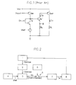
- Figure 1 shows an output terminal of electronic equipment comprising an output transistor Q out and a load R L .
- Vcc is a source of electric power.
- the switching transistor When an input signal processed by the electronic equipment triggers a switching transistor Q SW , the switching transistor is turned on or off. When the switching transistor Q SW is turned on, the output transistor is turned on. When the switching transistor Q SW is turned off, the output transistor is turned off.
- a diode D 1 connecting a transitor base with the collector is also turned on, and a constant-voltage source 4 loads a resistance R b with V ref voltage.
- the voltage at node A, V A is the same as the total of V ref and a diode voltage V D1 and the voltage at node B, V B is equal to the subtraction of the voltage between a base and an emitter of transistor Q 1 from node A voltage V A .
- V B is the same as V ref + V D1 - V BE , Q 1 and if V D1 is the same voltage as the V BE , Q1 V B can be V ref .
- the collector current of transistor Q 1 namely a base current I B of the output transistor Q out is the same as V B /R b which is V ref /R b , and I B is constant.
- I B is decided by the resistance R b and a constant voltage and is independent of the magnitude of the load R L of the output transistor Q out . So, regardless of load current I o an invariable base current I B flows and electric power is dissipated unnecessarily.
- EP-A-514980 discloses a driving circuit for a switching transistor comprising a detector for detecting a current dependent on the load current of the transistor and means to generate a base current to drive the transistor.
- EP-A-384513 discloses a circuit for regulating the base current of a semiconductor power device which acts to maintain constant the ratio between the emitter current and base current of the device.
- the present invention is directed to a base current-control circuit of an output transistor for maximizing efficiency in the use of electric power.
- This base current-control circuit of the output transistor controls the base current in accordance with the load current of the output transistor.
- a base current-control circuit of an output transistor comprising: a detector for detecting a load current of said output transistor, a base current generator for generating a base current to drive the output transistor, and characterised by a current-voltage converter for converting the detected current to an equivalent voltage, wherein the base current generator generates base current in accordance with ON/OFF signals of a switching transistor to drive the output transistor, by the use of the detected voltage and a reference voltage.
- Base current I B of an output transistor is shown as a simple linear function of a load current I O . So the load current, an independent variable, decides to the base current, a dependent variable. The base current is controlled by the load current.
- the load current of a driving terminal 8 connected to the output transistor is a detected current I sense detected by a load current detector.
- a current-voltage converter converts the detected current to equivalent voltage V sense .
- An output V ref from a constant-voltage source 4 and detected voltage V sense are input to a base current-control voltage generator, which outputs a base current-control voltage.
- the base current-control voltage is input to a switch.
- the signal from an output transistor ON/OFF controller is input to the switch and the base current-control voltage, via the switch, flows into a base current generator 7.
- the controlled base current I B from the base current generator 7 is input to the output transistor of a driving terminal 8.
- the base current I B is controlled by the load current.
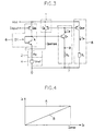
- FIG. 3 shows one embodiment of the present invention.
- a transistor Q S and an output transistor Q out are set up in parallel to detect the load current from the driving terminal 8.
- the output transistor Q out is a PNP type transistor.
- the transistor Q S for detecting the load current is also a PNP type.
- a detecting current I sense is decided by the rate of an emitter area between the transistor Q S and the output transistor Q out .
- I sense is K x I 0 .
- I sense changes in proportion to I o .
- V be,QS which is the voltage between the base and the emitter of the transistor Q S is the same as V be , Q out which is the voltage between the base and the emitter of the output transistor Q out .
- V T is the transistor thermal voltage
- I s is a saturation current
- K is the emitter area of Q S /the emitter area of Q out . Therefore, I c ,Q s , a collector current of Q s is K x I c ,Q out .
- K is in the range from 1/100 to 1/1000.
- Current-voltage converter 2 converts detected load current I sense to an equivalent voltage.
- resistance R s converts because the detected load current I sense flows into the resistance R s and then a voltage drop arises.
- the size of voltage is in proportion to the size of an inflow current.
- the detected voltage V sense is I sense x R s .
- a base current-control voltage generator 3 receiving the detected voltage V sense and reference voltage V ref outputs a base current-control voltage, which is applied to node C.
- Reference voltage V ref in series with resistance R s added to the voltage on resistance R s makes voltage on node C.
- reference voltage V ref is base current-control voltage of the output transistor in the absence of a load.
- V ref is fixed, so base current-control voltage V c changes in proportion to I sense and outputs to node C.
- V ref + K x I o x R s This is shown as V ref + K x I o x R s and it is a simple linear function of I o .
- base current-control voltage V c inputs to switch 6.
- the input signal is an output signal of the output transistor ON/OFF controller in internal electronic equipment.
- the switching transistor Q sw turns ON or OFF in accordance with these signals.
- base current-control voltage V c flows into the transistor Q 1 , a kind of buffer, and base current-control voltage appears on resistance R b connected to the emitter of NPN type transistor Q 1 .
- This current shows as V c /R b .
- a base current generator 7 of Figure 2 can be embodied in the transistor Q 1 as shown in Figure 3.
- a collector current of the transistor Q 1 that is, the base current I B of the output transistor is controlled by I o in the manner shown by formula 1.
- the voltage on node B is the sum of V ref and K x I o x R s .
- Figure 4 is a graph showing the operation characteristics compared with the prior art.
- the vertical and horizontal axes show respectively the base current I B and the load current I o .
- the base current I B is invariable regardless of the load current I o .
- the graph B indicates the base current I B .
- the output current is related to the load, which receives driving power from the suitable amount of base current I B .
Landscapes
- Engineering & Computer Science (AREA)
- Microelectronics & Electronic Packaging (AREA)
- Physics & Mathematics (AREA)
- Nonlinear Science (AREA)
- Electromagnetism (AREA)
- General Physics & Mathematics (AREA)
- Radar, Positioning & Navigation (AREA)
- Automation & Control Theory (AREA)
- Continuous-Control Power Sources That Use Transistors (AREA)
- Dc-Dc Converters (AREA)
- Electronic Switches (AREA)
Claims (8)
- Basisstromregelungsschaltung eines Ausgangstransistors (Qaus), umfassend: einen Detektor (Qs) zum Erfassen eines Laststroms des Ausgangstransistors, einen Basisstromgenerator (7) zur Erzeugen eines Basis-stroms für die Steuerung des Ausgangstransistors, und gekennzeichnet durch einen Strom-Spannungswandler (2) zum Umwandeln des erfaßten Stroms in eine äquivalente Spannung, wobei der Basisstromgenerator einen Basisstrom in Übereinstimmung mit EIN/AUS-Signalen eines Schalttransistors (QSCH) für die Steuerung des Ausgangstransistors unter Verwendung der erfaßten Spannung und einer Referenzspannung (Vref) erzeugt.
- Schaltung nach Anspruch 1, wobei der Laststromdetektor (Qs) einen Transistor desselben Leitungstyps wie der Ausgangstransistor (Qaus) umfaßt, um den Ausgangstransistor symmetrisch parallel zu steuern.
- Schaltung nach Anspruch 1 oder Anspruch 2, wobei der Strom-Spannungswandler, welcher den erfaßten Strom empfängt, einen Widerstand (Rs) umfaßt, der in Reihe mit einer Referenzspannung (Vref) geschaltet ist.
- Schalter nach einem der vorangehenden Ansprüche, wobei der Basisstrom die lineare Summe der Referenzspannung und der Erfassungsspannung ist, die dem Laststrom entspricht, und der Basisstrom zu dem Basisstromgenerator gesteuert wird, der einen Transistor (Q1) und einen an seinen Emitter angeschlossenen Widerstand (R6) umfaßt.
- Schalter nach einem der vorangehenden Ansprüche, wobei der Strom an dem Emitterwiderstand der Basisstrom des Ausgangstransistors ist und eine einfache lineare Funktion des Laststroms (Io) ist.
- Schalter nach einem der vorangehenden Ansprüche, wobei der Erfassungsstrom die Vervielfachung des Emitters des Transistors (Qs), welcher den Laststrom erfaßt, das Verhältnis der Emitterfläche im Ausgangstransistor und Io ist.
- Schalter nach einem der vorangehenden Ansprüche und ferner umfassend einen Steuersignalgenerator (3) zur Erzeugung einer Basistrom-Steuerspannung unter Verwendung der erfaßten Spannung und der Referenzspannung.
- Schaltung nach Anspruch 7, wobei ein Schaltmittel (QSCH), welches die Signale zu dem Steuerungsanschluß ausgibt, zwischen dem Basisstromgenerator und dem Basisstrom-Steuerspannungsgenerator ausgebildet ist.
Applications Claiming Priority (2)
| Application Number | Priority Date | Filing Date | Title |
|---|---|---|---|
| KR1019930001003 | 1993-01-27 | ||
| KR931003 | 1993-01-27 |
Publications (3)
| Publication Number | Publication Date |
|---|---|
| EP0608974A2 EP0608974A2 (de) | 1994-08-03 |
| EP0608974A3 EP0608974A3 (de) | 1994-10-12 |
| EP0608974B1 true EP0608974B1 (de) | 1998-09-16 |
Family
ID=19350024
Family Applications (1)
| Application Number | Title | Priority Date | Filing Date |
|---|---|---|---|
| EP94300106A Expired - Lifetime EP0608974B1 (de) | 1993-01-27 | 1994-01-07 | Basisstromreglungsschaltung eines Ausgangstransistors |
Country Status (5)
| Country | Link |
|---|---|
| US (1) | US5486781A (de) |
| EP (1) | EP0608974B1 (de) |
| JP (1) | JP3363980B2 (de) |
| CN (1) | CN1093996C (de) |
| DE (1) | DE69413266T2 (de) |
Families Citing this family (13)
| Publication number | Priority date | Publication date | Assignee | Title |
|---|---|---|---|---|
| DE4402340C1 (de) * | 1994-01-27 | 1995-05-24 | Bosch Gmbh Robert | Integrierte Schaltung |
| CN100341248C (zh) * | 2002-04-27 | 2007-10-03 | 盛群半导体股份有限公司 | 电流控制的电流/电压转换装置 |
| US7253678B2 (en) * | 2005-03-07 | 2007-08-07 | Analog Devices, Inc. | Accurate cascode bias networks |
| US8519788B2 (en) | 2010-04-19 | 2013-08-27 | Rf Micro Devices, Inc. | Boost charge-pump with fractional ratio and offset loop for supply modulation |
| DE102012111989A1 (de) | 2012-12-07 | 2014-06-12 | Flex-Elektrowerkzeuge Gmbh | Handgehaltene Schleifmaschine |
| WO2014186765A1 (en) | 2013-05-17 | 2014-11-20 | Cirrus Logic, Inc. | Single pin control of bipolar junction transistor (bjt)-based power stage |
| WO2014186776A1 (en) | 2013-05-17 | 2014-11-20 | Cirrus Logic, Inc. | Charge pump-based circuitry for bjt power supply |
| WO2015017317A2 (en) | 2013-07-29 | 2015-02-05 | Cirrus Logic, Inc. | Two terminal drive of bipolar junction transistor (bjt) for switch-mode operation of a light emitting diode (led)-based bulb |
| US9504106B2 (en) | 2013-07-29 | 2016-11-22 | Cirrus Logic, Inc. | Compensating for a reverse recovery time period of a bipolar junction transistor (BJT) in switch-mode operation of a light-emitting diode (LED)-based bulb |
| US20160164279A1 (en) * | 2014-12-09 | 2016-06-09 | Infineon Technologies Ag | Circuit and method for measuring a current |
| US9504118B2 (en) | 2015-02-17 | 2016-11-22 | Cirrus Logic, Inc. | Resistance measurement of a resistor in a bipolar junction transistor (BJT)-based power stage |
| US9609701B2 (en) | 2015-02-27 | 2017-03-28 | Cirrus Logic, Inc. | Switch-mode drive sensing of reverse recovery in bipolar junction transistor (BJT)-based power converters |
| US9603206B2 (en) | 2015-02-27 | 2017-03-21 | Cirrus Logic, Inc. | Detection and control mechanism for tail current in a bipolar junction transistor (BJT)-based power stage |
Family Cites Families (8)
| Publication number | Priority date | Publication date | Assignee | Title |
|---|---|---|---|---|
| US4213068A (en) * | 1978-01-30 | 1980-07-15 | Rca Corporation | Transistor saturation control |
| US4733163A (en) * | 1987-01-02 | 1988-03-22 | Motorola, Inc. | Digitally controlled current source |
| EP0369048A1 (de) * | 1988-11-15 | 1990-05-23 | Siemens Aktiengesellschaft | Schaltungsanordnung zur Laststromregelung in einem Leistungs-MOSFET |
| IT1228842B (it) * | 1989-02-21 | 1991-07-05 | Sgs Thomson Microelectronics | Circuito per la regolazione della corrente di base di un dispositivo di potenza a semiconduttore. |
| US5021687A (en) * | 1990-02-01 | 1991-06-04 | National Semiconductor Corporation | High speed inverting hysteresis TTL buffer circuit |
| IT1248607B (it) * | 1991-05-21 | 1995-01-19 | Cons Ric Microelettronica | Circuito di pilotaggio di un transistore di potenza con una corrente di base funzione predeterminata di quella di collettore |
| US5271399A (en) * | 1991-11-27 | 1993-12-21 | Trustees Of The University Of Pennsylvania | Three dimensional Fourier transform, fast spin echo, black blood magnetic resonance angtography |
| US5272392A (en) * | 1992-12-04 | 1993-12-21 | North American Philips Corporation | Current limited power semiconductor device |
-
1994
- 1994-01-05 JP JP00011694A patent/JP3363980B2/ja not_active Expired - Fee Related
- 1994-01-07 EP EP94300106A patent/EP0608974B1/de not_active Expired - Lifetime
- 1994-01-07 DE DE69413266T patent/DE69413266T2/de not_active Expired - Fee Related
- 1994-01-24 CN CN94100569A patent/CN1093996C/zh not_active Expired - Fee Related
- 1994-01-27 US US08/187,038 patent/US5486781A/en not_active Expired - Lifetime
Also Published As
| Publication number | Publication date |
|---|---|
| EP0608974A2 (de) | 1994-08-03 |
| JP3363980B2 (ja) | 2003-01-08 |
| CN1093996C (zh) | 2002-11-06 |
| CN1093508A (zh) | 1994-10-12 |
| US5486781A (en) | 1996-01-23 |
| DE69413266T2 (de) | 1999-04-01 |
| EP0608974A3 (de) | 1994-10-12 |
| JPH06252720A (ja) | 1994-09-09 |
| DE69413266D1 (de) | 1998-10-22 |
Similar Documents
| Publication | Publication Date | Title |
|---|---|---|
| EP0608974B1 (de) | Basisstromreglungsschaltung eines Ausgangstransistors | |
| JP2765716B2 (ja) | 直流電源装置の動作点制御装置 | |
| KR100281528B1 (ko) | 전원 공급 회로 | |
| EP0932858B1 (de) | Hybrider regler | |
| EP0580923A1 (de) | Schaltung zum Messen der auf reinen Spannungssollwert bezogenen Spannungsschwankungen für Fehlerverstärker enthaltende Vorrichtungen | |
| JP2006053898A (ja) | 過電流保護回路およびそれを利用した電圧生成回路ならびに電子機器 | |
| WO2006016456A1 (ja) | 回路の保護方法、保護回路およびそれを利用した電源装置 | |
| EP0896410B1 (de) | Überstromdetektorschaltung | |
| US6839254B2 (en) | Power supply with low loss making current limitation | |
| EP0662747B1 (de) | Gleichspannungswandler zur Ausgabe mehreren Signalen | |
| US6957278B1 (en) | Reference -switch hysteresis for comparator applications | |
| EP0730331A3 (de) | Schaltungsanordnung zur Begrenzung von Schaltüberspannungen an Leistungshalbleiterschaltern | |
| US6509723B2 (en) | Constant voltage regulator, method of controlling the same, and electric device provided with the same | |
| US20060152875A1 (en) | Overcurrent protection device | |
| JP2803151B2 (ja) | 電源装置 | |
| JP3309039B2 (ja) | インバータ制御装置の過電流保護回路 | |
| JP3255805B2 (ja) | スイッチング電源装置 | |
| US6150801A (en) | Regulator apparatus | |
| KR950009825Y1 (ko) | 출력트랜지스터의 베이스 전류 제어회로 | |
| JP2836382B2 (ja) | 直流電源 | |
| US7099162B2 (en) | Pulse-width-modulated signal to direct-current voltage converting unit | |
| KR940027274A (ko) | 전원 장치의 과전류 보호회로 | |
| RU1817178C (ru) | Устройство дл защиты от токовой перегрузки | |
| JPH04165410A (ja) | 直流電源装置 | |
| JPH06161574A (ja) | 電源装置 |
Legal Events
| Date | Code | Title | Description |
|---|---|---|---|
| PUAI | Public reference made under article 153(3) epc to a published international application that has entered the european phase |
Free format text: ORIGINAL CODE: 0009012 |
|
| AK | Designated contracting states |
Kind code of ref document: A2 Designated state(s): DE GB NL |
|
| PUAL | Search report despatched |
Free format text: ORIGINAL CODE: 0009013 |
|
| AK | Designated contracting states |
Kind code of ref document: A3 Designated state(s): DE GB NL |
|
| 17P | Request for examination filed |
Effective date: 19950301 |
|
| 17Q | First examination report despatched |
Effective date: 19970321 |
|
| GRAG | Despatch of communication of intention to grant |
Free format text: ORIGINAL CODE: EPIDOS AGRA |
|
| GRAG | Despatch of communication of intention to grant |
Free format text: ORIGINAL CODE: EPIDOS AGRA |
|
| GRAH | Despatch of communication of intention to grant a patent |
Free format text: ORIGINAL CODE: EPIDOS IGRA |
|
| GRAH | Despatch of communication of intention to grant a patent |
Free format text: ORIGINAL CODE: EPIDOS IGRA |
|
| GRAA | (expected) grant |
Free format text: ORIGINAL CODE: 0009210 |
|
| AK | Designated contracting states |
Kind code of ref document: B1 Designated state(s): DE GB NL |
|
| REF | Corresponds to: |
Ref document number: 69413266 Country of ref document: DE Date of ref document: 19981022 |
|
| PLBE | No opposition filed within time limit |
Free format text: ORIGINAL CODE: 0009261 |
|
| STAA | Information on the status of an ep patent application or granted ep patent |
Free format text: STATUS: NO OPPOSITION FILED WITHIN TIME LIMIT |
|
| 26N | No opposition filed | ||
| REG | Reference to a national code |
Ref country code: GB Ref legal event code: IF02 |
|
| PGFP | Annual fee paid to national office [announced via postgrant information from national office to epo] |
Ref country code: NL Payment date: 20090104 Year of fee payment: 16 Ref country code: DE Payment date: 20090123 Year of fee payment: 16 |
|
| PGFP | Annual fee paid to national office [announced via postgrant information from national office to epo] |
Ref country code: GB Payment date: 20090114 Year of fee payment: 16 |
|
| REG | Reference to a national code |
Ref country code: NL Ref legal event code: V1 Effective date: 20100801 |
|
| GBPC | Gb: european patent ceased through non-payment of renewal fee |
Effective date: 20100107 |
|
| PG25 | Lapsed in a contracting state [announced via postgrant information from national office to epo] |
Ref country code: NL Free format text: LAPSE BECAUSE OF NON-PAYMENT OF DUE FEES Effective date: 20100801 |
|
| PG25 | Lapsed in a contracting state [announced via postgrant information from national office to epo] |
Ref country code: DE Free format text: LAPSE BECAUSE OF NON-PAYMENT OF DUE FEES Effective date: 20100803 |
|
| PG25 | Lapsed in a contracting state [announced via postgrant information from national office to epo] |
Ref country code: GB Free format text: LAPSE BECAUSE OF NON-PAYMENT OF DUE FEES Effective date: 20100107 |