EP0609501A2 - Métallisation basé sur l'aluminium pour dispositif semi-conducteur - Google Patents
Métallisation basé sur l'aluminium pour dispositif semi-conducteur Download PDFInfo
- Publication number
- EP0609501A2 EP0609501A2 EP93118141A EP93118141A EP0609501A2 EP 0609501 A2 EP0609501 A2 EP 0609501A2 EP 93118141 A EP93118141 A EP 93118141A EP 93118141 A EP93118141 A EP 93118141A EP 0609501 A2 EP0609501 A2 EP 0609501A2
- Authority
- EP
- European Patent Office
- Prior art keywords
- wiring line
- concentration
- size
- alloy
- semiconductor device
- Prior art date
- Legal status (The legal status is an assumption and is not a legal conclusion. Google has not performed a legal analysis and makes no representation as to the accuracy of the status listed.)
- Granted
Links
Images

Classifications
-
- H—ELECTRICITY
- H10—SEMICONDUCTOR DEVICES; ELECTRIC SOLID-STATE DEVICES NOT OTHERWISE PROVIDED FOR
- H10P—GENERIC PROCESSES OR APPARATUS FOR THE MANUFACTURE OR TREATMENT OF DEVICES COVERED BY CLASS H10
- H10P14/00—Formation of materials, e.g. in the shape of layers or pillars
- H10P14/40—Formation of materials, e.g. in the shape of layers or pillars of conductive or resistive materials
- H10P14/412—Deposition of metallic or metal-silicide materials
-
- H—ELECTRICITY
- H10—SEMICONDUCTOR DEVICES; ELECTRIC SOLID-STATE DEVICES NOT OTHERWISE PROVIDED FOR
- H10W—GENERIC PACKAGES, INTERCONNECTIONS, CONNECTORS OR OTHER CONSTRUCTIONAL DETAILS OF DEVICES COVERED BY CLASS H10
- H10W20/00—Interconnections in chips, wafers or substrates
- H10W20/40—Interconnections external to wafers or substrates, e.g. back-end-of-line [BEOL] metallisations or vias connecting to gate electrodes
- H10W20/41—Interconnections external to wafers or substrates, e.g. back-end-of-line [BEOL] metallisations or vias connecting to gate electrodes characterised by their conductive parts
- H10W20/44—Conductive materials thereof
- H10W20/4403—Conductive materials thereof based on metals, e.g. alloys, metal silicides
- H10W20/4405—Conductive materials thereof based on metals, e.g. alloys, metal silicides the principal metal being aluminium
Definitions
- Aluminum is generally used for an electrode wiring line of a semiconductor device in view of a resistance or workability.
- a Cu-added Al alloy is generally used to prevent occurrence of an erroneous wiring line mode such as electro-migration or stress-migration, thereby improving reliability.
- the Al wiring line having a size of several fm larger than the size of Al crystal generally has a point where three grain boundaries between the Al grains overlap, i.e., a triple point of the grain boundaries.
- This phenomenon is called electro-migration. This is caused because the activation energy of the grain boundary of the Al-Cu alloy is about 1.4 eV while the activation energy of the grain boundary is about 0.6 eV, so that the grain boundary serves as a high-speed diffusion path.
- Cu is added to the Al alloy to segregate Cu at the grain boundaries and prevent the Al atoms from diffusing along the grain boundaries.
- the electro-migration life MTF [arb.unit] is prolonged depending on the content of Cu when the Cu concentration is about 8 wt% or less.
- the above-described triple points disappear in the wiring line, leaving bamboo-node-like grain boundaries across the grain size boundaries. More specifically, as the wiring line size becomes larger, the number of triple points of the grain boundaries per unit length is increased, as indicated by a line L2, so that electro-migration tends to occur. On the other hand, as the wiring line size becomes smaller, the number of bamboo-node-like grain boundaries is increased, as indicated by a line L1. The electro-migration life at this time depends on the diffusion speed within the crystal grain, MTF is improved as a whole, and the wiring line life tends to be prolonged.
- the line L1 represents the number of bamboo-node-like grain boundaries per unit length with respect to the line size
- the line L2 represents the number of triple points of the grain boundaries per unit with respect to the line size.
- MTF is improved when the Cu concentration is about 0.1 wt% or less. If the Cu concentration exceeds 0.1 wt%, MTF is degraded.
- the Cu concentration of the current wiring line is determined by the Cu concentration of a spattering target or vapor source, so that all the electrode wiring lines formed in the same process have the same Cu concentration.
- the electrode wiring lines having the same Cu concentration are used although each electrode wiring line ranging from a wiring line having a size in the submicron region to be used as a signal line to a wiring line having a size of 10 fm or more to be used as a power line has an optimal Cu concentration for its size.
- an optimal resistance to electro-migration for wiring lines having different sizes cannot be obtained.
- the present invention has been made to overcome the above drawback, and has as its object to provide a semiconductor device which selects and defines the Cu concentration of the electrode consisting of an Al alloy in accordance with the wiring line size, thereby obtaining an optimal resistance to electro-migration and high reliability.
- a semiconductor device comprising a wiring line formed from an electrode wiring layer using, as an electrode material, an Al alloy containing Cu, wherein a wiring line having a size smaller than a crystal grain size has a Cu concentration of 0.05 to 0.3 wt%, and a wiring line having a size larger than a crystal grain size has a Cu concentration of 0.5 to 10 wt%.
- the semiconductor of the present invention selects and defines the Cu concentration in the Al alloy wiring line in accordance with the wiring line size, thereby obtaining an optimal resistance to electro-migration.
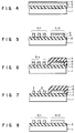
- Figs. 4 to 8 are views showing steps of manufacturing a semiconductor device according to an embodiment of the present invention.
- an Al-Cu alloy 3 serving as an electrode wiring line is formed on the surface of a semiconductor substrate 1 through an insulating film 2.
- a Cu-based material 4 e.g., pure Cu is formed on the Al-Cu alloy 3.
- film formation is performed by the sputtering method, the deposition method can be used in place of the sputtering method.
- the resultant structure constituted by stacking the Al-Cu alloy 3 and the Cu-based material 4 is formed into electrode wiring lines 3-1 and 3-2. More specifically, the wiring line 3-1 having a size smaller than the crystal grain size of the Al-Cu alloy 3 and the wiring line 3-2 having a size larger than the crystal grain size of the Al-Cu alloy 3 are formed to selectively expose the insulating film 2.
- a resist 5 is covered on a part of the exposed portion of the insulating film 2, and the Cu-based material 4.
- the Cu-based material 4 of the wiring line 3-1 having a size smaller than the crystal grain size of the Al-Cu alloy 3 is selectively removed by exposure and development to expose the thin wiring line 3-1.
- the resist 5 is covered on the thick wiring line 3-2.
- the thick wiring line 3-2 shown in Fig. 8 has a higher Cu concentration than that of the thin wiring line 3-1 by a diffusion amount.
- the Cu concentration of the Al-Cu alloy 3 in this embodiment is set in advance to be equal to that of the final wiring line 3-1 having a size smaller than the crystal grain size, the resistance to electro-migration of the wiring line 3-1 having a size smaller than the crystal grain size can be maximized, as shown in Fig. 3.
- Cu must not be segregated in the Al-Cu alloy 3 of the thin wiring line 3-1. Checking the segregated state of Cu, it was confirmed that Cu was not segregated by annealing when the Cu concentration was 0.3 wt% or less.
- the Cu concentration of the Al alloy wiring line having a size smaller than the crystal grain size was in a range of 0.05 to 0.3 wt%. Also in the Al-Cu alloy 3 of this embodiment, an optimal resistance to migration was obtained in a range of 0.05 to 0.3 wt% of the Cu concentration.
- the Cu-based material 4 is first covered on the Al-Cu alloy 3, and then the resultant structure is formed into the electrode wiring lines.
- the Al-Cu alloy 3 may be first formed into a desired electrode wiring line shape, and the Cu-based material 4 may be then covered and diffused.
- the Cu-based material is preferably annealed in the reducing atmosphere.
- annealing may be performed in an inert gas atmosphere as of N2 and Ar.
- the wiring line 3-2 having a size larger than the crystal grain size can obtain an optimal resistance to electro-migration at the Cu concentration of about 8 wt%.
- Cu must be segregated at the triple points where the grain boundaries in the Al-Cu alloy 3 overlap. It was confirmed that segregation was caused at the Cu concentration of 0.5 wt% or more by annealing.
- the optimal range of the Cu concentration of the wiring line 3-2 having a size larger than the crystal grain size is defined as 0.5 to 10 wt%.
- the final Cu concentration of the thick wiring line 3-2 can be set by defining the thickness of the Cu-based material 4 on the basis of the Cu concentration and the thickness of the Al-Cu alloy 3 such that a desired concentration is obtained.
- 800- ⁇ pure Cu is covered on a 1-fm thick Al-0.1wt% Cu alloy, and the manufacturing process in Figs. 4 and 5 is performed to obtain a thin wiring line 3-1 having a Cu concentration of 0.1 wt%, and a thick wiring line 3-2 having a Cu concentration of 8 wt%, thereby obtaining an optimal resistance to electro-migration.
- Al-Cu alloy is exemplified as the electrode wiring line
- other additive elements containing, e.g., Si may be used to obtain the same effect as described above.
Landscapes
- Internal Circuitry In Semiconductor Integrated Circuit Devices (AREA)
- Electrodes Of Semiconductors (AREA)
Applications Claiming Priority (3)
| Application Number | Priority Date | Filing Date | Title |
|---|---|---|---|
| JP7505/93 | 1993-01-20 | ||
| JP750593 | 1993-01-20 | ||
| JP750593 | 1993-01-20 |
Publications (3)
| Publication Number | Publication Date |
|---|---|
| EP0609501A2 true EP0609501A2 (fr) | 1994-08-10 |
| EP0609501A3 EP0609501A3 (fr) | 1994-11-09 |
| EP0609501B1 EP0609501B1 (fr) | 1999-09-15 |
Family
ID=11667648
Family Applications (1)
| Application Number | Title | Priority Date | Filing Date |
|---|---|---|---|
| EP93118141A Expired - Lifetime EP0609501B1 (fr) | 1993-01-20 | 1993-11-09 | Métallisation basé sur l'aluminium pour dispositif semi-conducteur |
Country Status (3)
| Country | Link |
|---|---|
| EP (1) | EP0609501B1 (fr) |
| KR (1) | KR0131287B1 (fr) |
| DE (1) | DE69326432T2 (fr) |
Cited By (2)
| Publication number | Priority date | Publication date | Assignee | Title |
|---|---|---|---|---|
| EP0701282A3 (fr) * | 1994-08-01 | 1996-10-30 | Motorola Inc | Structure d'interconnexion ayant une densité localisée de courant maximal réduite et procédé de fabrication d'un niveau d'interconnexion dans un dispositif semi-conducteur |
| EP0720219A3 (fr) * | 1994-12-30 | 1997-05-07 | At & T Corp | Fabrication d'une couche conductrice pour circuit intégré |
Family Cites Families (2)
| Publication number | Priority date | Publication date | Assignee | Title |
|---|---|---|---|---|
| JPS62114241A (ja) * | 1985-11-14 | 1987-05-26 | Fujitsu Ltd | 半導体装置 |
| JPH0284719A (ja) * | 1988-09-21 | 1990-03-26 | Nec Corp | 半導体装置の製造方法 |
-
1993
- 1993-11-09 EP EP93118141A patent/EP0609501B1/fr not_active Expired - Lifetime
- 1993-11-09 DE DE69326432T patent/DE69326432T2/de not_active Expired - Lifetime
-
1994
- 1994-01-19 KR KR1019940000939A patent/KR0131287B1/ko not_active Expired - Fee Related
Cited By (3)
| Publication number | Priority date | Publication date | Assignee | Title |
|---|---|---|---|---|
| EP0701282A3 (fr) * | 1994-08-01 | 1996-10-30 | Motorola Inc | Structure d'interconnexion ayant une densité localisée de courant maximal réduite et procédé de fabrication d'un niveau d'interconnexion dans un dispositif semi-conducteur |
| US5760476A (en) * | 1994-08-01 | 1998-06-02 | Motorola, Inc. | Interconnect run between a first point and a second point in a semiconductor device for reducing electromigration failure |
| EP0720219A3 (fr) * | 1994-12-30 | 1997-05-07 | At & T Corp | Fabrication d'une couche conductrice pour circuit intégré |
Also Published As
| Publication number | Publication date |
|---|---|
| KR0131287B1 (ko) | 1998-04-14 |
| DE69326432D1 (de) | 1999-10-21 |
| DE69326432T2 (de) | 2000-01-27 |
| EP0609501A3 (fr) | 1994-11-09 |
| EP0609501B1 (fr) | 1999-09-15 |
Similar Documents
| Publication | Publication Date | Title |
|---|---|---|
| EP0751567B1 (fr) | Alliages de cuivre pour des interconnexions de puces et procédé de fabrication | |
| EP0843895B1 (fr) | Methode de fabrication d'une structure d'interconnexion metallique pour circuit integre a fiabilite amelioree d'electromigration | |
| EP0269211A2 (fr) | Dispositif semi-conducteur avec une couche métallique | |
| US20060160350A1 (en) | On-chip Cu interconnection using 1 to 5 nm thick metal cap | |
| JPH0652788B2 (ja) | 集積半導体回路 | |
| US5567647A (en) | Method for fabricating a gate electrode structure of compound semiconductor device | |
| EP0130416B1 (fr) | Procédé pour former un contact ohmique sur un semi-conducteur du groupe III-V du type de conductivité N et composant semi-conducteur ayant un tel contact | |
| US5238874A (en) | Fabrication method for laminated films comprising Al-Si-Co alloy film and refractory metal silioide copper film | |
| US5296406A (en) | Aluminum alloy/silicon-chromium sandwich schottky diode | |
| US4942451A (en) | Semiconductor device having improved antireflection coating | |
| EP0609501A2 (fr) | Métallisation basé sur l'aluminium pour dispositif semi-conducteur | |
| US4502207A (en) | Wiring material for semiconductor device and method for forming wiring pattern therewith | |
| US5606203A (en) | Semiconductor device having Al-Cu wiring lines where Cu concentration is related to line width | |
| CA2112447A1 (fr) | Compose a resistivite electrique a la temperature ambiante comparable a celle du cuivre elementaire | |
| US5260604A (en) | Semiconductor device with improved immunity to contact and conductor defects | |
| JP3333306B2 (ja) | 半導体装置 | |
| EP0222795B1 (fr) | Traitement des polyciures dans la fabrication de semiconducteurs | |
| Liliental et al. | Electron microscopy study of the AuGe/Ni/Au contacts on GaAs and GaAlAs | |
| EP1001463A2 (fr) | Interconnexion d'aluminium ayant des sous- et sur-couches en titane pour circuits intégrés | |
| US5854116A (en) | Semiconductor apparatus | |
| JPH0156524B2 (fr) | ||
| EP1174918B1 (fr) | Procédé pour l'empêchement de transport de cuivre par une couche de piégeage pulverisée sur la face arrière d'une plaquette | |
| JP3270512B2 (ja) | 半導体装置の製造方法 | |
| JPH05291560A (ja) | 半導体デバイスのバリアメタル | |
| US6960306B2 (en) | Low Cu percentages for reducing shorts in AlCu lines |
Legal Events
| Date | Code | Title | Description |
|---|---|---|---|
| PUAI | Public reference made under article 153(3) epc to a published international application that has entered the european phase |
Free format text: ORIGINAL CODE: 0009012 |
|
| 17P | Request for examination filed |
Effective date: 19931109 |
|
| AK | Designated contracting states |
Kind code of ref document: A2 Designated state(s): DE FR GB |
|
| PUAL | Search report despatched |
Free format text: ORIGINAL CODE: 0009013 |
|
| AK | Designated contracting states |
Kind code of ref document: A3 Designated state(s): DE FR GB |
|
| 17Q | First examination report despatched |
Effective date: 19960205 |
|
| GRAG | Despatch of communication of intention to grant |
Free format text: ORIGINAL CODE: EPIDOS AGRA |
|
| GRAG | Despatch of communication of intention to grant |
Free format text: ORIGINAL CODE: EPIDOS AGRA |
|
| GRAH | Despatch of communication of intention to grant a patent |
Free format text: ORIGINAL CODE: EPIDOS IGRA |
|
| GRAH | Despatch of communication of intention to grant a patent |
Free format text: ORIGINAL CODE: EPIDOS IGRA |
|
| GRAA | (expected) grant |
Free format text: ORIGINAL CODE: 0009210 |
|
| AK | Designated contracting states |
Kind code of ref document: B1 Designated state(s): DE FR GB |
|
| REF | Corresponds to: |
Ref document number: 69326432 Country of ref document: DE Date of ref document: 19991021 |
|
| ET | Fr: translation filed | ||
| PLBE | No opposition filed within time limit |
Free format text: ORIGINAL CODE: 0009261 |
|
| STAA | Information on the status of an ep patent application or granted ep patent |
Free format text: STATUS: NO OPPOSITION FILED WITHIN TIME LIMIT |
|
| 26N | No opposition filed | ||
| REG | Reference to a national code |
Ref country code: GB Ref legal event code: IF02 |
|
| PGFP | Annual fee paid to national office [announced via postgrant information from national office to epo] |
Ref country code: FR Payment date: 20101123 Year of fee payment: 18 |
|
| PGFP | Annual fee paid to national office [announced via postgrant information from national office to epo] |
Ref country code: DE Payment date: 20101104 Year of fee payment: 18 |
|
| PGFP | Annual fee paid to national office [announced via postgrant information from national office to epo] |
Ref country code: GB Payment date: 20101103 Year of fee payment: 18 |
|
| GBPC | Gb: european patent ceased through non-payment of renewal fee |
Effective date: 20111109 |
|
| REG | Reference to a national code |
Ref country code: FR Ref legal event code: ST Effective date: 20120731 |
|
| REG | Reference to a national code |
Ref country code: DE Ref legal event code: R119 Ref document number: 69326432 Country of ref document: DE Effective date: 20120601 |
|
| PG25 | Lapsed in a contracting state [announced via postgrant information from national office to epo] |
Ref country code: GB Free format text: LAPSE BECAUSE OF NON-PAYMENT OF DUE FEES Effective date: 20111109 |
|
| PG25 | Lapsed in a contracting state [announced via postgrant information from national office to epo] |
Ref country code: FR Free format text: LAPSE BECAUSE OF NON-PAYMENT OF DUE FEES Effective date: 20111130 |
|
| PG25 | Lapsed in a contracting state [announced via postgrant information from national office to epo] |
Ref country code: DE Free format text: LAPSE BECAUSE OF NON-PAYMENT OF DUE FEES Effective date: 20120601 |