EP0609874A2 - Speicherschaltung mit einer Vielzahl von Eingangsignalen - Google Patents
Speicherschaltung mit einer Vielzahl von Eingangsignalen Download PDFInfo
- Publication number
- EP0609874A2 EP0609874A2 EP94101614A EP94101614A EP0609874A2 EP 0609874 A2 EP0609874 A2 EP 0609874A2 EP 94101614 A EP94101614 A EP 94101614A EP 94101614 A EP94101614 A EP 94101614A EP 0609874 A2 EP0609874 A2 EP 0609874A2
- Authority
- EP
- European Patent Office
- Prior art keywords
- gate
- input
- conductivity type
- type mos
- receiving
- Prior art date
- Legal status (The legal status is an assumption and is not a legal conclusion. Google has not performed a legal analysis and makes no representation as to the accuracy of the status listed.)
- Granted
Links
- 102100040862 Dual specificity protein kinase CLK1 Human genes 0.000 claims abstract description 42
- 101000749294 Homo sapiens Dual specificity protein kinase CLK1 Proteins 0.000 claims abstract description 32
- 102100040844 Dual specificity protein kinase CLK2 Human genes 0.000 claims abstract description 30
- 101000749291 Homo sapiens Dual specificity protein kinase CLK2 Proteins 0.000 claims abstract description 30
- 238000003475 lamination Methods 0.000 abstract description 22
- 230000006870 function Effects 0.000 description 12
- 238000010586 diagram Methods 0.000 description 6
- 230000000630 rising effect Effects 0.000 description 6
- 238000012360 testing method Methods 0.000 description 6
- 238000013461 design Methods 0.000 description 5
- 239000004065 semiconductor Substances 0.000 description 3
- 230000001960 triggered effect Effects 0.000 description 3
- 238000011156 evaluation Methods 0.000 description 2
- 238000000034 method Methods 0.000 description 2
- 230000007704 transition Effects 0.000 description 2
- 230000000903 blocking effect Effects 0.000 description 1
Images


Classifications
-
- G—PHYSICS
- G11—INFORMATION STORAGE
- G11C—STATIC STORES
- G11C7/00—Arrangements for writing information into, or reading information out from, a digital store
- G11C7/10—Input/output [I/O] data interface arrangements, e.g. I/O data control circuits, I/O data buffers
- G11C7/1078—Data input circuits, e.g. write amplifiers, data input buffers, data input registers, data input level conversion circuits
- G11C7/1093—Input synchronization
-
- G—PHYSICS
- G11—INFORMATION STORAGE
- G11C—STATIC STORES
- G11C7/00—Arrangements for writing information into, or reading information out from, a digital store
- G11C7/10—Input/output [I/O] data interface arrangements, e.g. I/O data control circuits, I/O data buffers
- G11C7/1078—Data input circuits, e.g. write amplifiers, data input buffers, data input registers, data input level conversion circuits
Definitions
- the present invention relates to a memory circuit, and, more particularly, to a multi-input memory circuit which has plural sets of clock signals and data signals and selectively uses an arbitrary set of clock and data signals to hold and output data.
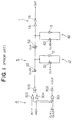
- Fig. 1 is a circuit diagram showing an example of a conventional memory circuit of the above type.
- This circuit has two systems of inputs (a data signal IN1 and clock signal CLK1, and a data signal IN2 and clock signal CLK2), and fixes the clock signal of a non-selected system to a logic value 1 so as to hold and output data of the selected system in synchronism with the rising edge of the clock signal of the selected system.
- This circuit mainly comprises an input circuit 4 and a latch 5 which is triggered at the rising edge of a clock signal.
- This latch 5 has a first input gate 22, which receives a signal from the input circuit 4 and is enabled or disabled by an inverted signal CLKB of a clock signal CLK, a first hold circuit 12, which receives a signal from this first input gate 22, a second input gate 52, which is enabled or disabled by the clock signal CLK, a second hold circuit 42, which receives a signal from the input circuit 4 or the first hold circuit 12 via the second input gate 52, and an output circuit 1.
- the one-input latch 5 designed as above holds and outputs data in synchronism with the rising edge of the clock signal.
- the first hold circuit 12 receives the output signal of the input circuit 4 from the first input gate 22, which is controlled by the inverted signal CLKB of the clock signal CLK, and holds the inverted signal of that input signal by means of a first feedback loop, which comprises a first inverting gate 2 and a first feedback gate 32.
- the second hold circuit 42 receives the output of the first hold circuit 12 from the second input gate 52, which is controlled by the clock signal CLK, and holds the inverted signal of that input signal or the value of the output signal from the input circuit 4 by means of a second feedback loop, which comprises a second inverting gate 3 and a second feedback gate 62.
- the output circuit 1, which has an inverter 1A and an inverter 1B, drives a load (not shown) at the subsequent stage and guarantees the function of the second feedback loop.
- the first inverting gate 2 and second inverting gate 3 have a structure of an inverter
- the first feedback gate 32 and second feedback gate 62 have a structure of a clocked inverter.
- the first input gate 22 and second input gate 52 both have a structure of a clocked inverter, and the first input gate 22 is enabled and the second input gate 52 is disabled during a period in which the clock signal CLK has a logic value 0. Accordingly, while the first feedback loop (first hold circuit 12) is holding the data signal, the second feedback loop (second hold circuit 42) keeps holding and outputting data of the previous cycle. While the clock signal CLK has a logic value 1, the first input gate 22 is disabled and the second input gate 52 is enabled. Accordingly, the data signal is cut off from the memory circuit and at the same time the data held in the first feedback loop (first hold circuit 12) is sent to the second feedback loop (second hold circuit 42). The second feedback loop (second hold circuit 42) holds and outputs this received data.
- the "clocked inverter” is a logic gate, which functions as an inverter only when the control signal has a logic value 1 and whose output has a high resistance when the control signal has a logic value 0.
- This input circuit 4 selects one system of data from two systems of data, and outputs it to the above-described one-input latch 5.
- the two systems of clock signals CLK1 and CLK2 input to this input circuit 4 are input to an AND gate, which comprises a NAND gate 301 and an inverter 302, to be converted into one system of a clock signal.
- the data signals IN1 and IN2 are input to a select gate, which comprises three NOR gates 303, 304 and 305, to be converted into one system of a data signal.
- This select gate has a structure of a multiplexer, which becomes active when the control signal has a logic value 0.
- the clock signal CLK2 is fixed to a logic value 1.
- the AND gate comprising the NAND gate 301 and inverter 302 always outputs the clock signal CLK1.
- the NOR gate 304 always outputs a logic value 0, causing the NOR gate 305 to always output the output of the NOR gate 304. That is, the clock signal CLK becomes the clock signal CLK1, and the output of the NOR gate 305 becomes the data signal IN1.
- the scan bus system is a method of evaluating the internal structure of an integrated circuit by connecting latches or registers to be evaluated in a row and outputting their contents as serial data. According to this method, while the individual latches hold and output received data in synchronism with a clock signal from the system in normal operation mode, each of the latches connected in a row shifts its content to the next latch, thereby outputting their contents as serial data, in synchronism with a test clock signal in test mode. Accomplishing this function, therefore, requires a memory circuit which selectively uses the logic connection in normal operation mode or the connection of the latches for the test mode.
- What relates to this invention is a memory circuit which is suitable particularly for the case where the normal operation or the test-mode operation is selected by the simplest system of disabling a test clock signal in normal operation mode and disabling a clock signal for the normal operation in test mode.
- the clock signal lags by a delay caused by traveling through the NAND gate 301 and inverter 302, so that the delay of the clock signal is wasted every cycle, as compared with an ordinary memory circuit of a single-system type.
- the skew and delay of the clock signal is always the bottleneck on the design in recent high-speed semiconductor integrated circuits, and the driver and the traveling path for the clock signal are designed very prudently. Therefore, the circuit configuration which causes the clock signal to pass through a gate and the circuit configuration which disturbs the regularity of that timing, as of the above-described conventional memory circuit, disadvantageously increase a burden on the circuit design.
- a multi-input memory circuit for receiving a plurality of clock signals and a plurality of data signals pared respectively with the plurality of clock signals, and selectively using an arbitrary set of clock and data signals to store and output data
- which circuit comprises a first input gate for receiving inverted signals of the plurality of clock signals and the plurality of data signals, and selectively outputting one of the plurality of data signals based on the plurality of the inverted signals of the clock signals; a first feedback loop having a first inverting gate and a first feedback gate having an input terminal connected to an output terminal of the first inverting gate and an output terminal connected to an input terminal thereof, the input terminal of the first inverting gate and the output terminal of the first feedback gate being connected to an output terminal of the first input gate; a second input gate for receiving an output of the first input gate and outputting the output after inversion; and a second feedback loop having a second inverting gate and a second feedback gate having an input terminal connected to an output terminal of the second inverting
- the first feedback gate includes a first transistor row having a series circuit having series-connected first conductivity type MOS transistors for receiving inverted signals of the plurality of clock signals respectively as gate inputs, and a first conductivity type MOS transistor for receiving an output of the first inverting gate as a gate input, the series circuit of first conductivity type MOS transistors being connected in series to the latter first conductivity type MOS transistor, and a second transistor row having a series circuit having series-connected second conductivity type MOS transistors for receiving the plurality of clock signals respectively as gate inputs, and an second conductivity type MOS transistor for receiving the output of the first inverting gate as a gate input, the series circuit of second conductivity type MOS transistors being connected in series to the latter second conductivity type MOS transistor, a drain electrode of a first end of the first transistor row and a drain electrode of a first end of the second transistor row being connected together to be an output terminal, a source electrode of a second end of the first transistor row being fixed to a potential of a high-potential
- control signal for the first input gate and the control signal for the second input gate work in the same phase, data dropout can be avoided.
- the logic value of the clock signal changes from "1" to "0”
- the second input gate is disabled at the same time, preventing any data dropout.
- this invention has such an advantage as to eliminate the need for fine adjustment for preventing data dropout and the need for re-checking.
- Fig. 2 presents a circuit diagram showing the first embodiment of the present invention.
- this embodiment has a clock signal CLK1, an inverted signal CLK1B of this clock signal CLK and a data signal IN1 as the first input system, and a clock signal CLK2, an inverted signal CLK2B of this clock signal CLK and a data signal IN2 as the second input system.
- the data signals IN1 and IN2 are respectively input to clocked inverters 111 and 112 whose outputs are both input to a first hold circuit 10 and a second input gate 50.
- the clocked inverters 111 and 112 are respectively controlled by the inverted signals CLK1B and CLK2B of the clock signals.
- the output of the second input gate 50 is input to a second hold circuit 40 and an output circuit 1.
- This output circuit like the one in Fig. 1, comprises an inverter 1A and an inverter 1B.
- the "vertical lamination inverter” is a logic gate having such a structure as that of a first feedback gate 30 of the first hold circuit 10, which comprises six MOS transistors 131, 132, 133, 134, 135 and 136 in Fig. 2. As illustrated, the three p channel (first conductivity type) MOS transistors 131, 132 and 133 are connected in series and are arranged in a row in vertical lamination, with one end of the transistor row connected to a power source potential.
- the three n channel MOS (second conductivity type) transistors 134, 135 and 136 are connected in series and are arranged in a row in vertical lamination, with one end of the transistor row connected to a ground potential. Both transistor rows are connected between the power source potential and the ground potential, constituting the vertical lamination inverter.
- the node between the first input gate 20 and the second input gate 50 is connected to the node between the transistors 133 and 136 of the first feedback gate 30, and is also connected via an inverter 2 to the control-signal input terminals of the transistors 132 and 135.
- the transistors 134 and 131 are respectively controlled by the first clock signal CLK1 and its inverted signal CLK1B, and the transistors 136 and 133 are respectively controlled by the second clock signal CLK2 and its inverted signal CLK2B. Therefore, the vertical lamination inverter functions as an inverter only when the clock signals CLK1 and CLK2 both have a logic value 1, and their outputs have a high resistance otherwise. Since this vertical lamination inverter is controlled by a clock signal which is in phase with the clock signal that controls the first input gate 20 constituted of the clocked inverters 111 and 112, no data dropout will occur in this memory circuit.
- the second input gate 50 comprises six MOS transistors 141, 142, 143, 144, 145 and 146, the first three being p channel MOS transistors and the second three being n channel MOS transistors, all connected between the power source potential and the ground potential.
- the transistors 141 and 143 are respectively controlled by the clock signals CLK1 and CLK2, while the transistors 144 and 146 are respectively controlled by the inverted signals CLK1B and CLK2B of those clock signals.
- the first input gate 20 is connected to the control-signal input terminals of the transistors 142 and 145, and the node between the transistors 143 and 146 is connected to the output circuit 1.
- the "horizontal lamination inverter” is a logic gate having such a structure as that of a second feedback gate 60 of the second hold circuit 40, which comprises six MOS transistors 161, 162, 163, 164, 165 and 166 in Fig. 2.
- the p channel MOS transistors 161 and 162 are connected in parallel and are arranged in horizontal lamination, with one end of the parallel circuit connected to the power source potential and the other end connected in series to the p channel MOS transistor 163 in vertical lamination.
- the n channel MOS transistors 164 and 165 are connected in parallel to be arranged in horizontal lamination, with one end of the parallel circuit connected to the ground potential with the other end connected in series to the n channel MOS transistor 166 in vertical lamination.
- the transistors 161-163 and the transistors 164-166 are connected between the power source potential and the ground potential, constituting a horizontal lamination inverter.
- the node between the second input gate 50 and the output circuit 1 is connected to the node between the transistors 163 and 166 of the second feedback gate 60, and is also connected via an inverter 3 to the control-signal input terminals of the transistors 163 and 166.
- the transistors 161 and 164 are respectively controlled by the first clock signal CLK1 and its inverted signal CLK1B, while the transistors 162 and 165 are respectively controlled by the second clock signal CLK2 and its inverted signal CLK2B. Therefore, the horizontal lamination inverter functions as an inverter when either one of the clock signals CLK1 and CLK2 has a logic value 1, and their outputs have a high resistance when those clock signals both have a logic value 0.
- This horizontal lamination inverter like the above-described vertical lamination inverter, functions in synchronism with the control clock signal of the first input gate 20.
- the first input gate 20 selects one of two systems of data signals.
- the clocked inverter 112 which is controlled by the inverted clock signal CLK2B, is always disabled, thus blocking the second data signal IN2 from the memory circuit.
- the first input gate 20 becomes equivalent to a clocked inverter which receives the first data signal IN1 as an input and is controlled by the inverted signal CLK1B of the first clock signal CLK1.
- the first feedback loop comprises the first inverting gate 2 and the transistors 131, 132, 133, 134, 135 and 136, which constitute the first feedback gate 30, and holds the output of the first input gate (clocked inverter 111) like the first feedback loop in the conventional memory circuit shown in Fig. 1.
- the transistors of the first feedback gate 30, which are respectively controlled by the clock signals CLK2 and CLK2B, are both enabled.
- the first feedback gate 30 is therefore equivalent to a clocked inverter which receives the output of the first inverting gate 2 as an input and is controlled by the first clock signal CLK1.
- the first feedback loop becomes equivalent to the first feedback loop in the conventional memory circuit shown in Fig. 1.
- the six MOS transistors 141 to 146 constituting the second input gate 50 transfers the output of the first input gate (inverting gate 111) to the second feedback loop.
- the transistors 143 and 146 which are respectively controlled by the clock signals CLK2 and CLK2B, are both enabled.
- the second input gate 50 is therefore equivalent to a clocked inverter which receives the output of the first input gate (clocked inverter 111) as an input and is controlled by the first signal CLK1.
- the second input gate 50 becomes equivalent to the second input gate 52 in the conventional memory circuit shown in Fig. 1.
- the second feedback loop comprises the second inverting gate 3 and the transistors 161 to 166, which constitute the second feedback gate 60, and holds the output of the second input gate 50 like the second feedback loop in the conventional memory circuit shown in Fig. 1.
- the transistors 162 and 165 which are respectively controlled by the clock signals CLK2 and CLK2B, are both disabled.
- the second feedback gate 60 is therefore equivalent to a clocked inverter which receives the output of the second inverting gate 3 as an input and is controlled by the first clock signal CLK1.
- the second feedback loop becomes equivalent to the second feedback loop in the conventional memory circuit shown in Fig. 1.
- the inverters 1A and 1B constitute an output buffer, and drive a load circuit at the next stage while reducing the load on the second feedback loop.
- this embodiment functions as an ordinary one-input memory circuit, which is triggered by the rising edge of the input, with the first data signal IN1 used as a data signal and the first clock signal CLK1 as a clock signal.
- this embodiment functions as an ordinary one-input memory circuit, which is triggered by the rising edge of the input, with the second data signal IN2 used as a data signal and the second clock signal CLK2 as a clock signal.
- control signal for the first input gate 20 functions in phase with the control signal for the second input gate 50 in this embodiment, data dropout will not occur.
- the logic value of the clock signal changes from "1" to "0”
- the second input gate is disabled at the same time, preventing any data dropout.
- the memory circuit embodying this invention will prevent data dropout.
- a p channel MOS transistor and an n channel MOS transistor conduct simultaneously due to the difference between their threshold values when a clock signal with a very dull waveform and its inverted signal are input, data dropout may occur. This comes to the matter of the difference in driving performances of the first feedback loop and the second input gate 50, and will not raise any problem on a practical waveform of the clock signal and the driving power of each gate.
- this embodiment will eliminate the need for fine adjustment for preventing data dropout and the need for re-checking.
- Fig. 3 presents a circuit diagram of the second embodiment.
- an inverting gate 6 is provided in place of the inverter 2 of the first embodiment, and a reset signal RSTB is added as an input.
- This embodiment performs the same function as the first embodiment when the reset signal RSTB has a logic value 1, but always outputs a logic value 0 when the reset signal RSTB has a logic value 0.
- first input gate 20, first feedback gate 30, second input gate 50, second inverting gate 3, second feedback gate 60 and output circuit 1 are identical to those of the first embodiment.
- the first inverting gate 6 receives the output of the first input gate 20 as one input and the reset signal RSTB as the other input.
- this gate 6 functions the same way as an inverter, so that this embodiment becomes an equivalent to the first embodiment.
- the reset signal RSTB has a logic value 0
- the first inverting gate 6 always outputs "1.” Therefore, the first feedback loop always holds a logic value 1, thus allowing the second feedback loop to always hold a logic value 0. Thus, this embodiment always outputs a logic value 0.
- this embodiment will function as a two-input rising-edge trigger type memory circuit which can reset the output by fixing the reset signal RSTB to a logic value 0.
- this invention can easily be adapted for a multi-system circuit by providing the vertically-laminated transistors in the vertical lamination inverter, which are controlled by the first and second control signals, in the same number of stages as the number of systems of clock signals, and providing the horizontally-laminated transistors in the horizontal lamination inverter, which are controlled by the first and second control signals, in the same number of stages as the number of systems of clock signals.
- a falling-edge trigger type memory circuit can easily be designed by replacing all the clock signals with their inverted signals and vice versa.
Landscapes
- Tests Of Electronic Circuits (AREA)
- Electronic Switches (AREA)
- Logic Circuits (AREA)
- Dram (AREA)
Applications Claiming Priority (2)
| Application Number | Priority Date | Filing Date | Title |
|---|---|---|---|
| JP5016010A JP2985554B2 (ja) | 1993-02-03 | 1993-02-03 | 記憶回路 |
| JP16010/93 | 1993-02-03 |
Publications (3)
| Publication Number | Publication Date |
|---|---|
| EP0609874A2 true EP0609874A2 (de) | 1994-08-10 |
| EP0609874A3 EP0609874A3 (de) | 1995-06-07 |
| EP0609874B1 EP0609874B1 (de) | 1999-01-07 |
Family
ID=11904622
Family Applications (1)
| Application Number | Title | Priority Date | Filing Date |
|---|---|---|---|
| EP94101614A Expired - Lifetime EP0609874B1 (de) | 1993-02-03 | 1994-02-02 | Speicherschaltung mit einer Vielzahl von Eingangsignalen |
Country Status (4)
| Country | Link |
|---|---|
| US (1) | US5377158A (de) |
| EP (1) | EP0609874B1 (de) |
| JP (1) | JP2985554B2 (de) |
| DE (1) | DE69415697T2 (de) |
Families Citing this family (4)
| Publication number | Priority date | Publication date | Assignee | Title |
|---|---|---|---|---|
| US5557581A (en) * | 1995-04-10 | 1996-09-17 | Sun Microsystems, Inc. | Logic and memory circuit with reduced input-to-output signal propagation delay |
| US6433603B1 (en) | 2000-08-14 | 2002-08-13 | Sun Microsystems, Inc. | Pulse-based high speed flop circuit |
| US6420903B1 (en) * | 2000-08-14 | 2002-07-16 | Sun Microsystems, Inc. | High speed multiple-bit flip-flop |
| TW200535857A (en) * | 2004-04-20 | 2005-11-01 | Innolux Display Corp | Dynamic shift register |
Family Cites Families (5)
| Publication number | Priority date | Publication date | Assignee | Title |
|---|---|---|---|---|
| JPS59151537A (ja) * | 1983-01-29 | 1984-08-30 | Toshiba Corp | 相補mos形回路 |
| JP2621993B2 (ja) * | 1989-09-05 | 1997-06-18 | 株式会社東芝 | フリップフロップ回路 |
| US5107465A (en) * | 1989-09-13 | 1992-04-21 | Advanced Micro Devices, Inc. | Asynchronous/synchronous pipeline dual mode memory access circuit and method |
| JPH0792495B2 (ja) * | 1990-06-25 | 1995-10-09 | 株式会社東芝 | スキャンパス付きフリップフロップ |
| JPH04121893A (ja) * | 1990-09-12 | 1992-04-22 | Mitsubishi Electric Corp | 半導体記憶装置 |
-
1993
- 1993-02-03 JP JP5016010A patent/JP2985554B2/ja not_active Expired - Lifetime
-
1994
- 1994-02-02 DE DE69415697T patent/DE69415697T2/de not_active Expired - Fee Related
- 1994-02-02 EP EP94101614A patent/EP0609874B1/de not_active Expired - Lifetime
- 1994-02-02 US US08/190,454 patent/US5377158A/en not_active Expired - Fee Related
Also Published As
| Publication number | Publication date |
|---|---|
| DE69415697D1 (de) | 1999-02-18 |
| JP2985554B2 (ja) | 1999-12-06 |
| EP0609874B1 (de) | 1999-01-07 |
| EP0609874A3 (de) | 1995-06-07 |
| DE69415697T2 (de) | 1999-07-29 |
| US5377158A (en) | 1994-12-27 |
| JPH06230087A (ja) | 1994-08-19 |
Similar Documents
| Publication | Publication Date | Title |
|---|---|---|
| US5896046A (en) | Latch structure for ripple domino logic | |
| US6421784B1 (en) | Programmable delay circuit having a fine delay element selectively receives input signal and output signal of coarse delay element | |
| EP2385626A1 (de) | Verringerung des unmittelbaren Spannungsabfalls während eines Abtast-Umschaltvorgangs | |
| US7129762B1 (en) | Efficient implementation of a bypassable flip-flop with a clock enable | |
| US7671633B2 (en) | Glitch free 2-way clock switch | |
| US5173626A (en) | Flip-flop with scan path | |
| US9081061B1 (en) | Scan flip-flop | |
| US5377158A (en) | Memory circuit having a plurality of input signals | |
| US6249141B1 (en) | Enhanced glitch removal circuit | |
| US20070063752A1 (en) | Master-slave flip flop | |
| US5638008A (en) | Method and apparatus for generating an asynchronously clocked signal in a synchronously clocked programmable device | |
| US7786758B2 (en) | Asynchronous clock gate with glitch protection | |
| US20050280442A1 (en) | Semiconductor integrated circuit | |
| US6005430A (en) | Clock skew circuit | |
| US12237837B2 (en) | Signal generation apparatus capable of rejecting noise | |
| JP2000009803A5 (de) | ||
| JP2025537950A (ja) | ホールド時間が改善された低面積フリップフロップアーキテクチャ | |
| KR950007337A (ko) | 디지탈적으로 조절가능하고 조정되어지는 지연 라인 및 방법 | |
| US7400178B2 (en) | Data output clock selection circuit for quad-data rate interface | |
| US11894845B1 (en) | Structure and method for delaying of data signal from pulse latch with lockup latch | |
| US20050076275A1 (en) | Integraged circuit and method for testing the integrated circuit | |
| KR0141803B1 (ko) | 멀티플렉서-래치 | |
| JPH05265949A (ja) | 集積回路装置 | |
| US20050151570A1 (en) | Integrated circuit having reduced substate bounce | |
| JPH10125056A (ja) | 半導体記憶装置 |
Legal Events
| Date | Code | Title | Description |
|---|---|---|---|
| PUAI | Public reference made under article 153(3) epc to a published international application that has entered the european phase |
Free format text: ORIGINAL CODE: 0009012 |
|
| AK | Designated contracting states |
Kind code of ref document: A2 Designated state(s): DE FR GB |
|
| PUAL | Search report despatched |
Free format text: ORIGINAL CODE: 0009013 |
|
| AK | Designated contracting states |
Kind code of ref document: A3 Designated state(s): DE FR GB |
|
| 17P | Request for examination filed |
Effective date: 19950427 |
|
| 17Q | First examination report despatched |
Effective date: 19970630 |
|
| GRAG | Despatch of communication of intention to grant |
Free format text: ORIGINAL CODE: EPIDOS AGRA |
|
| GRAG | Despatch of communication of intention to grant |
Free format text: ORIGINAL CODE: EPIDOS AGRA |
|
| GRAH | Despatch of communication of intention to grant a patent |
Free format text: ORIGINAL CODE: EPIDOS IGRA |
|
| GRAH | Despatch of communication of intention to grant a patent |
Free format text: ORIGINAL CODE: EPIDOS IGRA |
|
| GRAA | (expected) grant |
Free format text: ORIGINAL CODE: 0009210 |
|
| AK | Designated contracting states |
Kind code of ref document: B1 Designated state(s): DE FR GB |
|
| REF | Corresponds to: |
Ref document number: 69415697 Country of ref document: DE Date of ref document: 19990218 |
|
| ET | Fr: translation filed | ||
| PLBE | No opposition filed within time limit |
Free format text: ORIGINAL CODE: 0009261 |
|
| STAA | Information on the status of an ep patent application or granted ep patent |
Free format text: STATUS: NO OPPOSITION FILED WITHIN TIME LIMIT |
|
| 26N | No opposition filed | ||
| REG | Reference to a national code |
Ref country code: GB Ref legal event code: IF02 |
|
| PGFP | Annual fee paid to national office [announced via postgrant information from national office to epo] |
Ref country code: GB Payment date: 20020206 Year of fee payment: 9 |
|
| PGFP | Annual fee paid to national office [announced via postgrant information from national office to epo] |
Ref country code: FR Payment date: 20020212 Year of fee payment: 9 |
|
| PGFP | Annual fee paid to national office [announced via postgrant information from national office to epo] |
Ref country code: DE Payment date: 20020227 Year of fee payment: 9 |
|
| PG25 | Lapsed in a contracting state [announced via postgrant information from national office to epo] |
Ref country code: GB Free format text: LAPSE BECAUSE OF NON-PAYMENT OF DUE FEES Effective date: 20030202 |
|
| PG25 | Lapsed in a contracting state [announced via postgrant information from national office to epo] |
Ref country code: DE Free format text: LAPSE BECAUSE OF NON-PAYMENT OF DUE FEES Effective date: 20030902 |
|
| GBPC | Gb: european patent ceased through non-payment of renewal fee | ||
| PG25 | Lapsed in a contracting state [announced via postgrant information from national office to epo] |
Ref country code: FR Free format text: LAPSE BECAUSE OF NON-PAYMENT OF DUE FEES Effective date: 20031031 |
|
| REG | Reference to a national code |
Ref country code: FR Ref legal event code: ST |