EP0610058A2 - Dispositif pour supprimer les fluctuations de tension et les harmoniques - Google Patents
Dispositif pour supprimer les fluctuations de tension et les harmoniques Download PDFInfo
- Publication number
- EP0610058A2 EP0610058A2 EP94300723A EP94300723A EP0610058A2 EP 0610058 A2 EP0610058 A2 EP 0610058A2 EP 94300723 A EP94300723 A EP 94300723A EP 94300723 A EP94300723 A EP 94300723A EP 0610058 A2 EP0610058 A2 EP 0610058A2
- Authority
- EP
- European Patent Office
- Prior art keywords
- current
- compensation
- power
- value
- current instruction
- Prior art date
- Legal status (The legal status is an assumption and is not a legal conclusion. Google has not performed a legal analysis and makes no representation as to the accuracy of the status listed.)
- Granted
Links
Images

Classifications
-
- H—ELECTRICITY
- H02—GENERATION; CONVERSION OR DISTRIBUTION OF ELECTRIC POWER
- H02J—ELECTRIC POWER NETWORKS; CIRCUIT ARRANGEMENTS OR SYSTEMS FOR SUPPLYING OR DISTRIBUTING ELECTRIC POWER; SYSTEMS FOR STORING ELECTRIC ENERGY
- H02J3/00—Circuit arrangements for AC mains or AC distribution networks
- H02J3/01—Arrangements for reducing harmonics or ripples
-
- H—ELECTRICITY
- H02—GENERATION; CONVERSION OR DISTRIBUTION OF ELECTRIC POWER
- H02J—ELECTRIC POWER NETWORKS; CIRCUIT ARRANGEMENTS OR SYSTEMS FOR SUPPLYING OR DISTRIBUTING ELECTRIC POWER; SYSTEMS FOR STORING ELECTRIC ENERGY
- H02J3/00—Circuit arrangements for AC mains or AC distribution networks
- H02J3/18—Arrangements for adjusting, eliminating or compensating reactive power in networks
-
- Y—GENERAL TAGGING OF NEW TECHNOLOGICAL DEVELOPMENTS; GENERAL TAGGING OF CROSS-SECTIONAL TECHNOLOGIES SPANNING OVER SEVERAL SECTIONS OF THE IPC; TECHNICAL SUBJECTS COVERED BY FORMER USPC CROSS-REFERENCE ART COLLECTIONS [XRACs] AND DIGESTS
- Y02—TECHNOLOGIES OR APPLICATIONS FOR MITIGATION OR ADAPTATION AGAINST CLIMATE CHANGE
- Y02E—REDUCTION OF GREENHOUSE GAS [GHG] EMISSIONS, RELATED TO ENERGY GENERATION, TRANSMISSION OR DISTRIBUTION
- Y02E40/00—Technologies for an efficient electrical power generation, transmission or distribution
- Y02E40/30—Reactive power compensation
-
- Y—GENERAL TAGGING OF NEW TECHNOLOGICAL DEVELOPMENTS; GENERAL TAGGING OF CROSS-SECTIONAL TECHNOLOGIES SPANNING OVER SEVERAL SECTIONS OF THE IPC; TECHNICAL SUBJECTS COVERED BY FORMER USPC CROSS-REFERENCE ART COLLECTIONS [XRACs] AND DIGESTS
- Y02—TECHNOLOGIES OR APPLICATIONS FOR MITIGATION OR ADAPTATION AGAINST CLIMATE CHANGE
- Y02E—REDUCTION OF GREENHOUSE GAS [GHG] EMISSIONS, RELATED TO ENERGY GENERATION, TRANSMISSION OR DISTRIBUTION
- Y02E40/00—Technologies for an efficient electrical power generation, transmission or distribution
- Y02E40/40—Arrangements for reducing harmonics
Definitions
- This invention relates to a device for suppressing voltage fluctuation and higher harmonics. And more particularly, in a system wherein power is supplied from a power source system to a load of large power fluctuation and harmonic current, this invention relates to a device for suppressing voltage fluctuation and higher harmonics, that suppresses the voltage fluctuation and higher harmonics of the power source system that are created by the power fluctuation of the load.
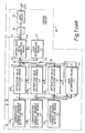
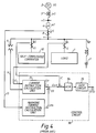
- Fig. 4 of the accompanying drawings shows a diagrammatic circuit layout of such a conventional device for suppressing voltage fluctuation and higher harmonics. To avoid complexity, the three-phase system is shown as a single-line connection diagram.
- a voltage fluctuation and higher harmonics suppression device constituted by a self-commutated converter 10 is arranged in parallel with load 1 and is controlled by a control circuit 30.
- a harmonic filter 7 is provided with the object of suppressing the higher harmonics generated by load 1 and improving the power factor.
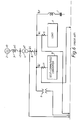
- Self-commutated converter 10 is constructed, as shown in Fig. 5, by AC reactors 12, gate turn-off thyristors (GTO) 13, diodes 14, and a DC capacitor 15.
- Control circuit 30 is constituted as follows. Specifically, it is equipped with: a current instruction calculation unit 31 that inputs a load current iL detected by a current transformer 5 and a system voltage V detected by a voltage detection transformer 6 and that finds a current instruction value iLo for suppressing voltage fluctuation; a harmonic current instruction calculation unit 32 that inputs a system current iS flowing in the power source system and detected by a current transformer 8 and that finds a harmonic current instruction value iHo for suppressing the higher harmonics emitted to the power source system; and an adder circuit 33 that adds current instruction values iLo and iHo.
- ACR automatic current signal regulator
- current instruction value iLo is a signal for compensating the load reactive power, but if required, a signal for compensating the negative phase sequence current of load 1 could be added.
- current instruction calculation unit 31 outputs a signal for compensating the negative phase sequence current of load 1 in addition to a signal for compensating the load reative power. Parts which are the same as in Fig. 4 are given the same reference numerals and a description of them is omitted.
- the load current iL of load 1 detected by current transformer 5 is the line current of the three-phase circuit.
- a three-phase/two-phase converter circuit 31A converts this three-phase AC current to two-phase AC current. This conversion is expressed by equation (1), where iR, iS and iT are the respective line currents of three-phase AC current iL and id and iq are the two-phase AC currents.
- Reactive power detection circuit 31D respectively inputs synchronized voltage signals vdo, vqo and two-phase AC currents id, iq, and detects instantaneous real power p and instantaneous imaginary power q. That is, reative power detection circuit 31D detects so-called instantaneous real power p and instantaneous imaginary power q as defined in "Journal of the Institute of Electrical Engineers of Japan, Article No. 58-B60, P41 to 48 "Theory of Generalization of Instantaneous Reactive Power and Its Applications". These are found by the calculation of equation (3).
- synchronous voltage signals vdo, vqo, in the two-phase AC are orthogonal components of magnitude 1pu; vd and vdo may be considered as practically equal, and vq and vqo may be considered as practically equal. Consequently, p also means the instantaneous active power supplied to load 1 from AC power source 2, while q also means the instantaneous reactive power circulating between the two phases. In this embodiment, only instantaneous reactive power q is used for calculating current instruction value iQo.
- Instantaneous imaginary power (instantaneous reative power) q is input to a filter 31E, which filters it, and a load reactive power QL is thereby found.
- a reative power instruction value QLo is found by multiplying load reactive power QL by a compensation gain KQ (fixed value), by a coefficient circuit 31F. This is then further converted to a current instruction value iQo By supplying it to an instantaneous current calculation circuit 31G.
- the calculation of current instruction value iQo is performed by inverse conversion of equation (3) and equation (1).
- three-phase AC load current iL detected by current transformer 5 is converted to two-phase AC currents id and iq by performing the calculation of equation (1) in a three-phase/two-phase conversion circuit 31H.
- Two-phase AC currents id and iq are then input to a negative phase sequence power detection circuit 31J, where negative phase sequence power is detected.
- the calculation is performed after inverting vqo (multiplied by -1), in the calculation of the instantaneous real power and instantaneous imaginary power using equation (3).
- the (-vqo) used in this calculation is obtained by inverting the polarity of output vqo of synchronous detection circuit 31C using an inverting circuit 31K.
- the fundamental wave positive phase sequence power is detected as the AC power of the doubled frequency of the fundamental wave frequency
- the fundamental wave negative phase sequence power is detected as DC power
- the fundamental wave negative phase sequence powers pN and qN can be obtained by filtering the outputs of negative phase sequence power detection circuit 31J by filters 31L and 31M.
- Negative phase sequence power instruction values pNo, qNo are found by multiplying fundamental wave negative phase sequence powers pN, qN by a compensating gain KN (fixed value) using coefficient circuits 31N, 31P respectively.
- a harmonic current instruction calculation unit 32 comprises a filter 32A and a coefficient circuit 32B.
- Current iS of the power source system detected by current transformer 8 is input to filter 32A which thereby detects a harmonic current iH.
- This is input to coefficient circuit 32B and multiplied by compensation gain KH (fixed value) to obtain a harmonic current instruction value iHo.
- harmonic current instruction calculation unit 32 is constructed with three R,S,T units corresponding to three-phase (R,S,T) components of system current iS. And, harmonic current instruction value iHo also includes three-phase (R,S,T) components.
- Reactive power current instruction value iQo, negative phase sequence current instruction value iNo and harmonic current instruction value iHo found as above are combined by adder circuit 33 to obtain current instruction value iCo for self-commutated converter 10. If explained in detail, three-phase (R,S,T) components of instruction values iQo, iNo and iHo are added to obtain three-phase (R,S,T) components of instruction value iCo, respectively.
- Output current iC of self-commutated converter 10 is made to track current instruction value iCo by current control performed by automatic current signal regulator 34 using the deviation between output current iC detected by current transformer 11 and current instruction value iCo found as above.
- the output of automatic current signal regulator 34 is input to gate circuit 35 which generates ON/OFF pulses for PWM control of self-commutated converter 10. ON/OFF pulses are then supplied to respective gates of GTOs 13 of self-commutated converter 10 shown in Fig. 5.
- a steel-making arc furnace is an example of a load 1 to be compensated by the voltage fluctuation and higher harmonics suppression device described above.
- reactive power, negative phase sequence current and harmonic current change irregularly with time, and their magnitudes are respectively very different depending on the condition of the material in the furnace.
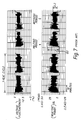
- Fig. 7 shows an example of a fluctuation of reactive power QL of an arc furnace (including leading-phase capacity), and a voltage fluctuation ⁇ V of the system. From this Figure, it can be seen that the range of fluctuation of the reative power is different at the commencement of melting of the material (scrap) (melting period) and after melting of the material has been fully completed (refining period).
- the range of fluctuation of the reative power in the refining period, shown as QL2 in the Figure is less than one half that in the melting period, shown as QL1 in the Figure, and the range of fluctuation of the voltage is proportional to this. Though not shown in the Figure, it is found that there is the same tendency to the above regarding the negative phase sequence current and harmonic current also.
- compensation gains KQ, KN and KH used in finding respective current instruction values iQo, iNo and iHo are fixed.
- this capacity is determined to be fairly large. However, since the range of fluctuation in the refining period is small, there is no possibility that output of the suppression device reaches the rated capacity. If this is considered over the period of one heat cycle, although the rated capacity is fully utilized in the melting period (about one-third of the heat cycle), in the remaining period i.e. the refining period, only about one-half of the rated capacity is utilized, which is uneconomic.
- the capacity of the suppression device of voltage fluctuation and higher harmonics is determined such as to limit these within two certain limiting values.
- the capacity of the voltage fluctuation and higher harmonics suppression device is smaller than the maximum amount of fluctuation such as of the reactive power in the melting period. If now we provisionally assume that the capacity of the suppression device is made one-half of the maximum amount of fluctuation of the reactive power, there is the problem that, when compensation gain KQ is 1, the current instruction value of the suppression deive in the melting period will exceed the rated value.
- compensation gain KQ must be made smaller than 1 (e.g. 0.5). In this case, there is the problem that, as described above, the utilization rate of the suppression device in the refining period is poor.
- one object of this invention is to provide a device for suppressing voltage fluctuation and higher harmonics that is capable of effectively utilizing the device capacity to the maximum extent irrespective of the magnitude of load fluctuation, thereby improving economy, and that is capable of improving the suppression effect of voltage fluctuation and higher harmonics.
- the device includes a self-commutated converter arranged in parallel with the load and a control circuit for controlling the self-commutated converter.
- the control circuit includes a compensation current variable calculation circuit for calculating a plurality of compensation current variables based on electrical quantities of the power source system and the load, a compensation gain calculation circuit for determining at least one compensation gain based on at least one of the compensation current variable, and a current instruction value calculation circuit for calculating a plurality of respective current instruction values based on the compensation gain and a plurality of the respective current compensation variables.
- the control circuit also includes an overall current instruction value calculation circuit for calculating an overall current instruction value by combining the current instruction values, and a current control circuit for controlling an output current of the self-commutated converter based on the overall current instruction value.
- a device for suppressing voltage fluctuation and higher harmonics of a power source system which supplies power to a load with large power fluctuation and large harmonic current.
- the device is constructed as described above.
- the device further includes an overall compensation gain calculation circuit for determining an overall compensation gain based on the overall current instruction value, and a final current instruction value calculation circuit for calculating a final current instruction value by multiplying the overall current instruction value and the overall compensation gain.
- the overall compensation gain is determined such that the final current instruction value does not exceed a rated current value of the self-commutated converter.
- the current control circuit controls the output current of the self-commutated converter based on the final current instruction value in place of the overall current instruction value.
- the device includes a self-commutated converter arranged in parallel with the load, and a control circuit for controlling the self-commutated converter.
- the control circuit includes a compensation current variable calculation circuit for calculating a plurality of compensation current variables based on electrical quantities of the power source system and the load, a current instruction value calculation circuit for calculating a plurality of respective current instruction values based on a plurality of the respective compensation current variables, an overall current instruction value calculation circuit for calculating an overall current instruction value by combining the plurality of current instruction values.
- the control circuit further includes an overall compensation gain calculation circuit for determining an overall compensation gain based on the overall current instruction value, a final current instruction value calculation circuit for calculating a final current instruction value by multiplying the overall current instruction value and the overall compensation gain, and a current control circuit for controlling an output current of the self-commutated converter based on the final current instruction value.
- the overall compensation gain is determined such that said final current instruction value does not exceed a rated current value of the self-commutated converter.
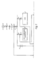
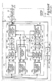
- control circuit 20 is composed of: a plurality of compensation current detection means (in the Figure, as an example, three compensation current variable detection means 21A to 21C); gain determining means (1) 22 that determines respective compensation gains K1, K2, K3 for detected outputs which are compensation current variables i1, i2, i3 in accordance with the magnitudes of their outputs i1, i2, i3; instruction value calculation means (23A, 23B, 23C in Fig.
- correction means 26 of the overall current instruction value and means 25 that determines its compensation gain are omitted.
- compensation gain of compensation gain determining means 22 could be determined with reference to a specified compensation current component, for example compensation current variable i1, or could be determined with reference to two specified compensation current components, for example compensation current variables i1 and i2.
- correction means 26 of the overall current instruction value and means 25 are provided and wherein gain determining means (1) 22 is omitted and instruction value calculation means 23A, 23B and 23C calculates respective current instruction values i1o, i2o and i3o based on fixed compensation gains, respectively.
- a plurality of compensation current detection means 21A, 21B, 21C calculate respective compensation current variables i1, i2 and i3 using the electrical quantities of the power source system and load 1 (e.g. system voltage V, system current iS, and load current iL).
- Gain determining means (1) 22 determines respective compensation gains K1, K2, K3 in accordance with the magnitude of compensation current variables i1, i2 and i3 such that none of the current instruction values i1o, i2o, i3o of the respective components gets too large.
- Instruction value calculation means 23A, 23B, 23C calculate respective current instruction values i1o, i2o, i3o by multiplying respective compensation current variables i1, i2, i3 by compensation gains K1, K2, K3. These are then combined by adder circuit 24 to calculate overall current instruction value iCo.
- Gain determining means (2) 25 determines overall compensation gain KC in accordance with the magnitude of overall current instruction value iCo such that overall current instruction value iCo of self-commutated converter 10 does not exceed its rated value.
- Instruction value compensation means 26 calculates final current instruction value iCoe by multiplying overall current instruction value iCo by overall compensation gain KC.
- Automatic current signal regulator (ACR) 34 controls gate circuit 35 such that output current iC of self-commutated converter 10 detected by current transformer 11 and final current instruction value iCoe coincide.
- compensation current variables i1, i2 and i3 current itself may be used in some case. But usually, as a compensation current variable for reative power component, a reactive power (QL) of load 1 is used. As a compensation current variable for negative phase sequence current component, an instantaneous real power pN and an instantaneous imaginary power qN of a fundamental wave negative phase sequence power are used.
- a harmonic current iH of the power source system is usually used.
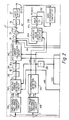
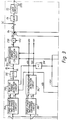
- Fig. 2 is a circuit diagram showing a specific example of a first embodiment of this invention.
- the system layout (main circuit) is the same as that of Fig. 6, which shows the prior art, so further description of it is omitted, and explanation thereof is also omitted.
- control circuit 20 also, parts which are the same as parts in Fig. 6 are given the same reference numerals and an explanation of them is omitted.
- coefficient circuits 31N, 31P in the prior art control circuit 30 shown in Fig. 6 are dispensed with, and the following construction is added. Specifically, outputs pN, qN of filters 31L, 31M are input to an absolute value detection circuit (1) 22A for the negative phase sequence power; output PN of absolute value detection circuit 22A is input to a hold circuit (1) 22B; PNmax which is the output of hold circuit 22B is input to a gain determining circuit (1) 22C; gain (-KN) which is the output of gain determining circuit (1) 22C and the output of instantaneous current calculating circuit 31Q are multiplied by a multiplier circuit 23; and the result of the multiplication is input to adder circuit 24.
- overall current instruction value iCo which is the result of the addition performed by adder circuit 24 and outputs vdo, vqo of synchronization detection circuit 31C are input to an absolute value detection circuit (2) 25A; an output PCo of absolute value detection circuit 25A is input to a hold circuit (2) 25B; PCmaxo, which is the output of this hold circuit (2) 25B, is input to a gain determining circuit (2) 25C; gain KC which is the output of gain determining circuits 25C, and overall current instruction value iCo which is the result of the addition performed by adder circuit 24, are input to multiplier circuit 26; and the deviation between final current instruction value iCoe which is thereby obtained and current iC detected by current transformer 11 is input to automatic current signal regulator 34.
- Gain determining circuit 22C determines compensation gain KN for negative phase sequence current instruction value iNo of instantaneous current calculation circuit 31Q in accordance with maximum value PNmax.
- Negative phase sequence current instruction value iNo is calculated in multiplier circuit 23 by multiplying compensation gain KN of the negative phase sequence current found as above by negative phase sequence current detection value iN.
- Adder circuit 24 finds overall current instruction value iCo by adding current instruction value iQo for the reactive power, harmonic current instruction value iHo, and negative phase sequence current instruction value iNo. Next, final current instruction value iCoe is determined such that the rated current of self-commutated converter 10 is not exceeded. This is implemented by the following technique. First of all, absolute value PCo of overall current instruction value iCo is found by absolute value detection circuit 25A, which receives signals vdo, vqo and instruction value iCo. In this calculation, the instantaneous real and imaginary powers pCo, qCo are calculated by substituting three phase components of overall current instruction value iCo into equation (1) and equation (3). Absolute value PCo is then found in equation (6) by substituting pCo and qCo in place of pN and qN, respectively.
- Absolute value PC of overall current instruction value iCo also varies with time with fluctuation in load 1, so hold circuit 25B holds its maximum value PCmax for a fixed time (on the order of several tens of ms to one second).
- Gain determining circuit 25C calculates overall compensation gain KC based on maximum value PCmaxo held for a fixed time by hold circuit 25B. This technique is the same for gain determining circuit 22C as described above.
- Final current instruction value iCoe is found by multiplying overall current instruction value iCo and overall compensation gain KC in multiplier 26.
- Automatic current signal regulator (ACR) 34 controls gate circuit 35 such that output current iC of self-commutated converter 10 coincides with final current instruction value iCoe.
- the first embodiment described above has the following benefits due to its action as described above.
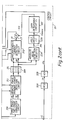
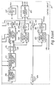
- Absolute value detection circuit (2) 22D is a means that calculates an absolute value PH of harmonic current iH
- hold circuit (2) 22E is a means that holds a maximum value PHmax of this for a fixed time.
- Absolute value detection circuit (2) 22D receives harmonic current iX from filter 32A and synchronous voltage signals vdo, vqo from synchronous detection circuit 31C and outputs absolute value PH of harmonic current iH.
- Hold circuit (2) 22E receives absolute value PH and outputs maximum value PHmax.
- Circuit 22D, 22E have identical constructions with absolute value detection circuit (2) 25A and hold circuit (2) 25B in Fig. 2, respectively.
- Hold circuit (3) 22F is identical in its construction with hold circuit (1) 22B and is the means that holds for a fixed time maximum value QLmax of reactive power detection value QL from filter 31E.
- Instantaneous current calculation circuit 31G receives reactive power detection value QL from filter 31E and voltage signals vdo, vqo and converts them to a current instruction value iQ as in the prior art control circuit 30 except that QLo and iQo are substituted by QL and iQ, respectively.
- Gain determining circuit 22G is a means for determining compensation gains KQ, KN, and KH for respective current instruction values iQo, iNo and iHo in accordance with reactive power component maximum value QLmax, negative phase sequence component maximum value PNmax, and harmonic component maximum value PHmax. It is constituted, for example, by the following procedures.
- the rated capacity of self-commutated converter 10 is assumed to be PC, and, for the purposes of explanation, it is assumed that QLmax > PHmax > PNmax.
- ACR 34 controls gate circuit 35 such that output current iC of self-commutated converter 10 coincides with overall current instruction value iCo.
- target gain of gain determining circuit 22G need not necessarily be 1, but could have different values for each component.
- compensation gain KN for negative phase sequence current component is only calculated in gain determining circuit 22C. And as other compensation gains KQ and KH, fixed values are used respectively.
- compensation gain KQ for reactive power component and compensation gain KN for negative phase sequence current component may be calculated based on compensation current variables such as reactive power QL, instantaneous real and imaginary powers pN and qN of a fundamental wave negative phase sequence power. And as only compensation gain KH a fixed value is used.
- control circuit 20 may be used, wherein as compensation gains KQ, KN and KH, fixed gains are used, respectively, and wherein gain determining means (2) 25 and instruction value compensation means 26 in Figure 1 are provided in control circuit 20.
- a voltage fluctuation and higher harmonics suppression device can be provided wherein the device capacity can be effectively utilized to the maximum and economy thereby improved irrespective of the magnitude of the load fluctuations, and wherein the voltage fluctuation and higher harmonics suppression effect can be improved.
Landscapes
- Engineering & Computer Science (AREA)
- Power Engineering (AREA)
- Supply And Distribution Of Alternating Current (AREA)
- Control Of Electrical Variables (AREA)
- Power Conversion In General (AREA)
- Networks Using Active Elements (AREA)
Applications Claiming Priority (2)
| Application Number | Priority Date | Filing Date | Title |
|---|---|---|---|
| JP17307/93 | 1993-02-04 | ||
| JP05017307A JP3130694B2 (ja) | 1993-02-04 | 1993-02-04 | 電圧変動及び高調波の抑制装置 |
Publications (3)
| Publication Number | Publication Date |
|---|---|
| EP0610058A2 true EP0610058A2 (fr) | 1994-08-10 |
| EP0610058A3 EP0610058A3 (en) | 1994-08-24 |
| EP0610058B1 EP0610058B1 (fr) | 1998-05-06 |
Family
ID=11940358
Family Applications (1)
| Application Number | Title | Priority Date | Filing Date |
|---|---|---|---|
| EP94300723A Expired - Lifetime EP0610058B1 (fr) | 1993-02-04 | 1994-02-01 | Dispositif pour supprimer les fluctuations de tension et les harmoniques |
Country Status (4)
| Country | Link |
|---|---|
| US (1) | US5586018A (fr) |
| EP (1) | EP0610058B1 (fr) |
| JP (1) | JP3130694B2 (fr) |
| DE (1) | DE69409987T2 (fr) |
Cited By (4)
| Publication number | Priority date | Publication date | Assignee | Title |
|---|---|---|---|---|
| WO1999063639A1 (fr) * | 1998-06-04 | 1999-12-09 | Aerospatiale Societe Nationale Industrielle | Systeme de compensation des harmoniques dans un reseau electrique |
| EP1324459B1 (fr) * | 2001-12-28 | 2014-11-12 | Toshiba Mitsubishi-Electric Industrial Systems Corporation | Compensateur de puissance réactive |
| CN105531594A (zh) * | 2014-03-10 | 2016-04-27 | 富士电机株式会社 | 电流检测器和电力变换装置 |
| EP3511797A4 (fr) * | 2016-09-30 | 2020-06-03 | Daikin Industries, Ltd. | Dispositif de filtre actif, dispositif de climatisation et système de climatisation |
Families Citing this family (10)
| Publication number | Priority date | Publication date | Assignee | Title |
|---|---|---|---|---|
| US5751138A (en) * | 1995-06-22 | 1998-05-12 | University Of Washington | Active power conditioner for reactive and harmonic compensation having PWM and stepped-wave inverters |
| US6862199B2 (en) * | 2001-02-01 | 2005-03-01 | Northeastern University | Adaptive controller for d-statcom in the stationary reference frame to compensate for reactive and harmonic distortion under unbalanced conditions |
| SE523039C2 (sv) * | 2001-11-28 | 2004-03-23 | Abb Ab | Förfarande och anordning för kompensering av en industriell lasts förbrukning av reaktiv effekt |
| JP2004180363A (ja) * | 2002-11-25 | 2004-06-24 | Tm T & D Kk | 電力系統の逆相分電圧補償システム |
| US7309973B2 (en) * | 2006-04-24 | 2007-12-18 | Power Conservation Ltd | Mitigation of harmonic currents and conservation of power in non-linear load systems |
| JP5018380B2 (ja) * | 2007-10-02 | 2012-09-05 | 富士電機株式会社 | 無効電力補償装置の制御方式 |
| JP4989499B2 (ja) * | 2008-01-28 | 2012-08-01 | 株式会社日立製作所 | 電力変換装置 |
| JP5281329B2 (ja) * | 2008-07-25 | 2013-09-04 | 本田技研工業株式会社 | インバータ発電機 |
| EP3620886A4 (fr) * | 2017-05-30 | 2020-09-23 | Daikin Industries, Ltd. | Système de gestion de qualité d'alimentation électrique et climatiseur |
| JP6909867B2 (ja) * | 2017-11-30 | 2021-07-28 | 株式会社東芝 | 電圧補償装置 |
Family Cites Families (6)
| Publication number | Priority date | Publication date | Assignee | Title |
|---|---|---|---|---|
| JPH0834669B2 (ja) * | 1986-06-26 | 1996-03-29 | 三菱電機株式会社 | 高調波抑制装置 |
| JPS6366617A (ja) * | 1986-09-09 | 1988-03-25 | Toshiba Corp | 無効電力補償装置 |
| JP2714195B2 (ja) * | 1989-12-08 | 1998-02-16 | 株式会社東芝 | 電圧変動及び高調波の抑制装置 |
| JP2760646B2 (ja) * | 1990-09-18 | 1998-06-04 | 株式会社東芝 | 電力変換装置の電流指令値演算装置 |
| JP2728575B2 (ja) * | 1991-06-14 | 1998-03-18 | 株式会社日立製作所 | 電力変換方法及び装置 |
| US5738247A (en) * | 1996-09-25 | 1998-04-14 | Kuan; Ching Fu | Automatic liquid material metering system |
-
1993
- 1993-02-04 JP JP05017307A patent/JP3130694B2/ja not_active Expired - Lifetime
-
1994
- 1994-02-01 EP EP94300723A patent/EP0610058B1/fr not_active Expired - Lifetime
- 1994-02-01 DE DE69409987T patent/DE69409987T2/de not_active Expired - Lifetime
-
1995
- 1995-09-28 US US08/535,348 patent/US5586018A/en not_active Expired - Lifetime
Cited By (7)
| Publication number | Priority date | Publication date | Assignee | Title |
|---|---|---|---|---|
| WO1999063639A1 (fr) * | 1998-06-04 | 1999-12-09 | Aerospatiale Societe Nationale Industrielle | Systeme de compensation des harmoniques dans un reseau electrique |
| FR2779583A1 (fr) * | 1998-06-04 | 1999-12-10 | Aerospatiale | Systeme antipollution pour reseau electrique |
| EP1324459B1 (fr) * | 2001-12-28 | 2014-11-12 | Toshiba Mitsubishi-Electric Industrial Systems Corporation | Compensateur de puissance réactive |
| CN105531594A (zh) * | 2014-03-10 | 2016-04-27 | 富士电机株式会社 | 电流检测器和电力变换装置 |
| EP3511797A4 (fr) * | 2016-09-30 | 2020-06-03 | Daikin Industries, Ltd. | Dispositif de filtre actif, dispositif de climatisation et système de climatisation |
| US10797584B2 (en) | 2016-09-30 | 2020-10-06 | Daikin Industries, Ltd. | Active filter device, air conditioning device, and air conditioning system |
| AU2017336736B2 (en) * | 2016-09-30 | 2020-10-22 | Daikin Industries, Ltd. | Active filter device, air conditioning device, and air conditioning system |
Also Published As
| Publication number | Publication date |
|---|---|
| JP3130694B2 (ja) | 2001-01-31 |
| US5586018A (en) | 1996-12-17 |
| JPH06233464A (ja) | 1994-08-19 |
| DE69409987D1 (de) | 1998-06-10 |
| DE69409987T2 (de) | 1998-09-10 |
| EP0610058B1 (fr) | 1998-05-06 |
| EP0610058A3 (en) | 1994-08-24 |
Similar Documents
| Publication | Publication Date | Title |
|---|---|---|
| Kamran et al. | Combined deadbeat control of a series-parallel converter combination used as a universal power filter | |
| Acuna et al. | Improved active power filter performance for renewable power generation systems | |
| Ramos et al. | Incremental passivity control in multilevel cascaded H-bridge converters | |
| EP0492396B1 (fr) | Système d'onduleur en parallèle | |
| Liang et al. | A power-line conditioner based on flying-capacitor multilevel voltage-source converter with phase-shift SPWM | |
| Mortezaei et al. | Grid-connected symmetrical cascaded multilevel converter for power quality improvement | |
| EP0610058B1 (fr) | Dispositif pour supprimer les fluctuations de tension et les harmoniques | |
| Chebabhi et al. | Comparative study of reference currents and DC bus voltage control for Three-Phase Four-Wire Four-Leg SAPF to compensate harmonics and reactive power with 3D SVM | |
| Caseiro et al. | Cooperative and dynamically weighted model predictive control of a 3-level uninterruptible power supply with improved performance and dynamic response | |
| EP0239278B1 (fr) | Appareil capacitif pour la compensation de puissance réactive | |
| Tan et al. | Droop controlled microgrid with DSTATCOM for reactive power compensation and power quality improvement | |
| EP0431967B1 (fr) | Dispositif pour supprimer les fluctuations de tension et les harmoniques | |
| Hasan et al. | Online harmonic extraction and synchronization algorithm based control for unified power quality conditioner for microgrid systems | |
| Ghanbarian et al. | Design and implementation of a new modified sliding mode controller for grid-connected inverter to controlling the voltage and frequency | |
| Koushki et al. | A model predictive control for a four-leg inverter in a stand-alone microgrid under unbalanced condition | |
| Chen et al. | Direct power control of DSTATCOMs for voltage flicker mitigation | |
| Xavier et al. | Adaptive saturation scheme for a multifunctional single-phase photovoltaic inverter | |
| RU2442275C1 (ru) | Способ управления трехфазным статическим преобразователем при несимметричной нагрузке | |
| Lin | A single-phase three-level pulsewidth modulation AC/DC converter with the function of power factor corrector and active power filter | |
| Qasim et al. | ADALINE based control strategy for three-phase three-wire UPQC system | |
| RU2741061C1 (ru) | Система управления многоуровневым активным фильтром | |
| RU2573599C1 (ru) | Устройство компенсации высших гармоник и коррекции несимметрии сети | |
| Jena et al. | Comparative study between different control strategies for shunt active power filter | |
| Oliveira et al. | Switching frequency reduction for efficiency optimization in two paralleled UPS systems | |
| RU2677628C1 (ru) | Трехфазный компенсатор реактивной мощности |
Legal Events
| Date | Code | Title | Description |
|---|---|---|---|
| PUAI | Public reference made under article 153(3) epc to a published international application that has entered the european phase |
Free format text: ORIGINAL CODE: 0009012 |
|
| PUAL | Search report despatched |
Free format text: ORIGINAL CODE: 0009013 |
|
| 17P | Request for examination filed |
Effective date: 19940214 |
|
| AK | Designated contracting states |
Kind code of ref document: A2 Designated state(s): DE FR GB SE |
|
| AK | Designated contracting states |
Kind code of ref document: A3 Designated state(s): DE FR GB SE |
|
| RHK1 | Main classification (correction) |
Ipc: H02J 3/01 |
|
| 17Q | First examination report despatched |
Effective date: 19950606 |
|
| GRAG | Despatch of communication of intention to grant |
Free format text: ORIGINAL CODE: EPIDOS AGRA |
|
| GRAG | Despatch of communication of intention to grant |
Free format text: ORIGINAL CODE: EPIDOS AGRA |
|
| GRAH | Despatch of communication of intention to grant a patent |
Free format text: ORIGINAL CODE: EPIDOS IGRA |
|
| GRAH | Despatch of communication of intention to grant a patent |
Free format text: ORIGINAL CODE: EPIDOS IGRA |
|
| GRAA | (expected) grant |
Free format text: ORIGINAL CODE: 0009210 |
|
| AK | Designated contracting states |
Kind code of ref document: B1 Designated state(s): DE FR GB SE |
|
| PG25 | Lapsed in a contracting state [announced via postgrant information from national office to epo] |
Ref country code: FR Free format text: LAPSE BECAUSE OF FAILURE TO SUBMIT A TRANSLATION OF THE DESCRIPTION OR TO PAY THE FEE WITHIN THE PRESCRIBED TIME-LIMIT Effective date: 19980506 |
|
| REF | Corresponds to: |
Ref document number: 69409987 Country of ref document: DE Date of ref document: 19980610 |
|
| PG25 | Lapsed in a contracting state [announced via postgrant information from national office to epo] |
Ref country code: SE Free format text: LAPSE BECAUSE OF FAILURE TO SUBMIT A TRANSLATION OF THE DESCRIPTION OR TO PAY THE FEE WITHIN THE PRESCRIBED TIME-LIMIT Effective date: 19980806 |
|
| EN | Fr: translation not filed | ||
| PGFP | Annual fee paid to national office [announced via postgrant information from national office to epo] |
Ref country code: GB Payment date: 19990204 Year of fee payment: 6 |
|
| PLBE | No opposition filed within time limit |
Free format text: ORIGINAL CODE: 0009261 |
|
| STAA | Information on the status of an ep patent application or granted ep patent |
Free format text: STATUS: NO OPPOSITION FILED WITHIN TIME LIMIT |
|
| 26N | No opposition filed | ||
| PG25 | Lapsed in a contracting state [announced via postgrant information from national office to epo] |
Ref country code: GB Free format text: LAPSE BECAUSE OF NON-PAYMENT OF DUE FEES Effective date: 20000201 |
|
| GBPC | Gb: european patent ceased through non-payment of renewal fee |
Effective date: 20000201 |
|
| PGFP | Annual fee paid to national office [announced via postgrant information from national office to epo] |
Ref country code: DE Payment date: 20130131 Year of fee payment: 20 |
|
| REG | Reference to a national code |
Ref country code: DE Ref legal event code: R071 Ref document number: 69409987 Country of ref document: DE |
|
| REG | Reference to a national code |
Ref country code: DE Ref legal event code: R071 Ref document number: 69409987 Country of ref document: DE |
|
| PG25 | Lapsed in a contracting state [announced via postgrant information from national office to epo] |
Ref country code: DE Free format text: LAPSE BECAUSE OF EXPIRATION OF PROTECTION Effective date: 20140204 |