EP0610066A1 - Multiplicateur de capacitance pour la compensation interne de fréquence de circuits intégrés régulateurs à découpage - Google Patents
Multiplicateur de capacitance pour la compensation interne de fréquence de circuits intégrés régulateurs à découpage Download PDFInfo
- Publication number
- EP0610066A1 EP0610066A1 EP94300746A EP94300746A EP0610066A1 EP 0610066 A1 EP0610066 A1 EP 0610066A1 EP 94300746 A EP94300746 A EP 94300746A EP 94300746 A EP94300746 A EP 94300746A EP 0610066 A1 EP0610066 A1 EP 0610066A1
- Authority
- EP
- European Patent Office
- Prior art keywords
- inverting input
- capacitance
- inverting
- frequency
- circuit
- Prior art date
- Legal status (The legal status is an assumption and is not a legal conclusion. Google has not performed a legal analysis and makes no representation as to the accuracy of the status listed.)
- Granted
Links
- 239000003990 capacitor Substances 0.000 claims abstract description 25
- 230000008878 coupling Effects 0.000 claims description 2
- 238000010168 coupling process Methods 0.000 claims description 2
- 238000005859 coupling reaction Methods 0.000 claims description 2
- 238000010586 diagram Methods 0.000 description 5
- 230000001105 regulatory effect Effects 0.000 description 3
- 230000001939 inductive effect Effects 0.000 description 2
- 238000006842 Henry reaction Methods 0.000 description 1
- 238000002955 isolation Methods 0.000 description 1
- 229910052710 silicon Inorganic materials 0.000 description 1
- 239000010703 silicon Substances 0.000 description 1
Images
Classifications
-
- H—ELECTRICITY
- H03—ELECTRONIC CIRCUITRY
- H03H—IMPEDANCE NETWORKS, e.g. RESONANT CIRCUITS; RESONATORS
- H03H11/00—Networks using active elements
- H03H11/46—One-port networks
- H03H11/48—One-port networks simulating reactances
- H03H11/483—Simulating capacitance multipliers
-
- H—ELECTRICITY
- H03—ELECTRONIC CIRCUITRY
- H03H—IMPEDANCE NETWORKS, e.g. RESONANT CIRCUITS; RESONATORS
- H03H11/00—Networks using active elements
- H03H11/46—One-port networks
- H03H11/48—One-port networks simulating reactances
Definitions
- This invention relates to switching voltage regulators constituted as integrated circuits.
- op-amp capacitance multiplying operational amplifier
- the invention provides a capacitance multiplying circuit for use on an integrated circuit chip for providing a relatively large on-chip capacitance useful in loop frequency compensation functions, said circuit comprising: an operational amplifier having inverting and non-inverting inputs, a single ended output and a unity gain frequency; a resistive connection between the inverting and non-inverting inputs; means for coupling the output of the operational amplifier to its inverting input; and means for driving the non-inverting input at a frequency that is below the said unity gain frequency whereby a relatively large equivalent shunt capacitance is present at the said non-inverting input.
- the invention also provides a capacitance multiplying circuit comprising a high gain differential amplifier having an output directly connected to an inverting input of the amplifier and a resistor connected between the inverting input and a non-inverting input of the amplifier and adapted to exhibit at the non-inverting input a capacitance related in value to the resistance value of said resistor.
- a switching regulator is operated at a relatively high switching frequency and incorporates an error amplifier that requires a relatively large compensation capacitor.
- An op-amp with its small internal compensation capacitor has its output connected to its inverting input and includes a first resistor connected across its input terminals.
- a second resistor couples the non-inverting input of the capacitance multiplying op-amp to the regulator's error amplifier output to add an R and equivalent C frequency compensation to it.
- the capacitance multiplying op-amp's non-inverting input presents an equivalent capacitance inversely proportional to the value of the first resistor multiplied by unity gain frequency of the op-amp. This produces a substantial capacitance as an on-chip component and the second resistor provides a series resistor loop compensation component.
- the equivalent capacitor and the second resistor in series represent the frequency compensating element of the whole switching regulator on the output of the error amplifier.
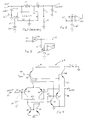
- Figure 1 is a schematic block diagram of one example of a known voltage boosting switching voltage regulator.
- FIG. 1 is an equivalent circuit representation of the circuit of the invention.
- Figure 3 is a block diagram showing how the circuit of the invention is associated with a switching regulator amplifier.
- Figure 4 is a schematic diagram of the circuit of the invention.
- Integrated circuit (IC) switching voltage regulators are popular because of their high performance, versatility and economy.
- the LM1577 is typical of such a voltage regulator. It is designed to operate with a five-volt input and switch at about 52 kHz. It has an adjustment capability which permits the user to control the output voltage.
- Figure 1 shows an application of the LM1577 which produces a 12 volt output at up to 800 ma. The circuit functions to maintain the 12 volt output independent of load and input voltage fluctuations.
- box 10 represents an LM1577.
- the numbers inside the box represent the pin numbers of a five-pin TO-220 IC package.
- a +5 volt input is applied to terminal 11 (pin 5) with ground return at terminal 12 (pin 3).
- a relatively low value (0.1 ⁇ f) capacitor 13 is connected to the input power line to provide input decoupling.
- An inductor 14, which has a typical value of about 100 ⁇ henries, is coupled between IC pins 5 and 4.
- a Schottky power diode 15 is coupled between inductor 14 and output terminal 16 at which the regulated output voltage will appear.
- a large-value filter capacitor (several hundred microfarads) 19 is coupled between output terminal 16 and round.
- Resistors 17 and 18 act as a voltage divider across the regulated output at terminal 16 to produce a feedback that is applied to IC pin 2.
- Resistor 21 and capacitor 20 are coupled between IC pin 1 and ground to provide frequency compensation for the regulator.
- the regulator contains a switch which periodically switches pin 4 to ground. When this switch is closed the current flowing in inductor 14 will ramp up. When this switch opens the switch current will fall to zero and the inductor will generate an inductive kickback in a polarity that adds to the potential at terminal 11. Rectifier 15 will pass the inductive kickback to charge capacitor 19 to a level above that of terminal 5. The boosted voltage on capacitor 19 will be a function of the average voltage at pin 4. Therefore, the charge on capacitor 19 will be a function of the regulator duty cycle. When the potential across capacitor 19 exceeds a value, which produces about 1.3 volts at pin 2, the regulator switch pulse width is reduced.
- resistor 18 When resistor 18 is 2k ohms and resistor 17 is 17.4k ohms, a 12 volt output will be maintained at terminal 16. Thus, the feedback to pin 2 will control the switching pulse width thereby regulating the output voltage even though the input voltage or the load connected to the regulator vary.
- Capacitor 20 is relatively large in terms of IC components. It will typically have a value of the order of nanofarads and must therefore be an off-chip component. It would be desirable to incorporate the regulator loop compensation elements in these and analogous circumstances entirely within the integrated circuit chip.
- FIG. 2 illustrates by way of example a basic circuit conforming to of the invention.
- Op-amp 22 has its output coupled back to its inverting input and a resistor 23 is connected between the inverting and non-inverting inputs.
- the op-amp presents an equivalent capacitance 20' at its non-inverting input.
- the capacitor 20' is shown in dashed outline because it is an effective capacitance, not an actual element.
- the circuit of Figure 2 can easily simulate a capacitor having a value on the order of several nanofarads. Such a value would otherwise involve inordinate chip area if fabricated as an on-chip capacitance.
- Figure 3 shows how the circuit of Figure 2 is applied as part of the loop compensation in a switching regulator error amplifier 26. Where the circuit elements are the same as those of Figure 2, the same numerals are employed.
- Error amplifier 26 represents the high gain transconductance amplifier which is part of a switching regulator such as element 10 of Figure 1.
- This amplifier is the circuit element that compares the feedback on pin 2 with an internal reference and drives the circuits that control the switch duty cycle.
- amplifier 26 has an output at terminal 27 that can be frequency compensated, either by a discrete resistor and capacitor, or by the invention of utilizing an IC resistor and a relatively large equivalent capacitance. As described above, capacitance 20' is presented at terminal 24. This creates the nanofarad-sized capacitor 20 of Figure 1. Resistor 21 then completes the loop compensation circuit on the output of error amplifier 26. Since the circuit of the invention can be realized, using small area IC components, it is feasible to form the circuit of Figure 3 as an entirely on-chip structure. This removes the requirement of off-chip compensation components.
- FIG 4 is a schematic diagram showing how op-amp 22, of Figure 3, can be implemented for an IC chip.
- This circuit constitutes the preferred embodiment of the invention.
- the heart of the circuit is a pair of PNP transistors 29 and 30 which respectively form the non-inverting and inverting inputs of op-amp 22.
- NPN transistors 31 and 32 respectively form the input and output transistors of a conventional current mirror load for the differential input stage.
- the single ended output of the input stage appears at the collector of transistor 32 which is directly connected to the base of common emitter transistor amplifier 33.
- Transistor 35 acts an emitter follower isolating buffer which couples the collector of transistor 33 to the base of emitter follower output transistor 36. This isolation ensures very high voltage gain in transistor 33.
- the op-amp's own small frequency compensation capacitor 34 is connected between the base and collector of transistor 33. This capacitor is needed in the op-amp to ensure the amplifier's unity gain stability. Its typical value is about 20 pf.
- Resistors 37 and 38 act in series as the emitter load for output transistor 36. These resistors form a voltage divider so that node 39 forms the output of op-amp 22. This node is directly connected to the inverting input so that 100% negative feedback is present as shown in the block diagrams of Figures 2 and 3.
- Transistor 40 forms a plural output current source. Its emitter is returned to the +V CC rail by resistor 41. The base of transistor 40 is returned to a V BIAS terminal 42 which is operated at a potential that produces the desired current outputs. Transistor 40 is shown as a four collector device which is typically a lateral PNP transistor having four equal quadrant collectors. Typically, the value of V BIAS is selected to produce one microampere in each of the collectors. Thus, transistor 35 receives two microamperes, transistor 33 receives one microampere and the differential input stage operates at a tail current of one microampere.
- the circuit of Figure 4 was constructed in the form of monolithic silicon, planar and PN junction isolated integrated circuit components. The following values were employed: COMPONENT VALUE Resistor 21 7.5k ohms Resistor 23 300 ohms Resistor 37 6.2k ohms Resistor 38 22k ohms Capacitor 34 20pf
- the circuit was operated from a 2.5 volt supply and node 27 was at 0.8 volt.
- the V BIAS was set for one microampere in each of the transistor 40 collectors.
- the op-amp had a unity gain frequency of 100 kHz.
- node 24 When driven at 1 kHz, node 24 displayed an equivalent shunt capacitance 20' of about 5.3 nf. This, in combination with resistor 19, can provide an effective loop frequency compensation for IC switching regulators.
- the entire circuit dissipated less than 0.1 microwatt at a supply potential of 2.5 volts.
Landscapes
- Amplifiers (AREA)
- Dc-Dc Converters (AREA)
- Networks Using Active Elements (AREA)
Applications Claiming Priority (2)
| Application Number | Priority Date | Filing Date | Title |
|---|---|---|---|
| US13508 | 1979-02-21 | ||
| US08/013,508 US5382918A (en) | 1993-02-04 | 1993-02-04 | Capacitance multiplier for the internal frequency compensation of switching regulator integrated circuits |
Publications (2)
| Publication Number | Publication Date |
|---|---|
| EP0610066A1 true EP0610066A1 (fr) | 1994-08-10 |
| EP0610066B1 EP0610066B1 (fr) | 1998-06-03 |
Family
ID=21760326
Family Applications (1)
| Application Number | Title | Priority Date | Filing Date |
|---|---|---|---|
| EP94300746A Expired - Lifetime EP0610066B1 (fr) | 1993-02-04 | 1994-02-01 | Multiplicateur de capacitance pour la compensation interne de fréquence de circuits intégrés régulateurs à découpage |
Country Status (4)
| Country | Link |
|---|---|
| US (1) | US5382918A (fr) |
| EP (1) | EP0610066B1 (fr) |
| JP (1) | JP3320883B2 (fr) |
| DE (1) | DE69410649T2 (fr) |
Cited By (6)
| Publication number | Priority date | Publication date | Assignee | Title |
|---|---|---|---|---|
| EP1215807A1 (fr) * | 2000-12-08 | 2002-06-19 | Micrel Incorporated | Addition d'un zéro d'une transformée de laplace dans un circuit linéaire pour stabilisation de fréquence |
| US6724257B2 (en) | 2002-07-31 | 2004-04-20 | Micrel, Inc. | Error amplifier circuit |
| EP1387478A3 (fr) * | 2002-07-31 | 2004-05-12 | Micrel Incorporated | Addition d'un zéro d'une transformée de Laplace dans un circuit linéaire pour stabilisation de fréquence |
| US6737841B2 (en) | 2002-07-31 | 2004-05-18 | Micrel, Inc. | Amplifier circuit for adding a laplace transform zero in a linear integrated circuit |
| CN110048601A (zh) * | 2019-05-29 | 2019-07-23 | 电子科技大学 | 一种有源电容电路 |
| CN113904656A (zh) * | 2021-12-09 | 2022-01-07 | 上海芯龙半导体技术股份有限公司 | 一种等效电容模块、等效电容电路及芯片 |
Families Citing this family (18)
| Publication number | Priority date | Publication date | Assignee | Title |
|---|---|---|---|---|
| US5502370A (en) * | 1994-09-06 | 1996-03-26 | Motorola, Inc. | Power factor control circuit having a boost current for increasing a speed of a voltage control loop and method therefor |
| US5514947A (en) * | 1995-01-31 | 1996-05-07 | National Semiconductor Corporation | Phase lead compensation circuit for an integrated switching regulator |
| US6546059B1 (en) * | 1999-12-28 | 2003-04-08 | Intel Corporation | Adaptive integrated PLL loop filter |
| US6344772B1 (en) * | 2000-06-06 | 2002-02-05 | Agere Systems Guardian Corp | Apparatus and method for capacitance multiplication |
| US6304067B1 (en) | 2000-12-08 | 2001-10-16 | Micrel, Incorporated | Adding a laplace transform zero to a linear integrated circuit for frequency stability |
| US6650070B1 (en) | 2002-07-25 | 2003-11-18 | Varon Lighting, Inc. | Point of use lighting controller |
| US6930526B1 (en) | 2003-12-04 | 2005-08-16 | National Semiconductor Corporation | Quasi-feedforward PWM modulator |
| JP4171784B2 (ja) * | 2004-09-09 | 2008-10-29 | トレックス・セミコンダクター株式会社 | 位相補償回路及びこれを有する電源回路 |
| US7385448B2 (en) * | 2006-05-17 | 2008-06-10 | Intelleflex Corporation | Circuitry for adaptively generating and using a reference voltage |
| US20090306311A1 (en) | 2008-06-05 | 2009-12-10 | The Administrators Of The Tulane Educational Fund | Methods and instrumentation for during-synthesis monitoring of polymer functional evolution |
| US8311785B2 (en) * | 2006-11-02 | 2012-11-13 | Texas Instruments Incorporated | Methods and apparatus to minimize saturation in a ground fault detection device |
| US7834636B2 (en) * | 2006-11-02 | 2010-11-16 | Texas Instruments Incorporated | Methods and apparatus to facilitate ground fault detection with a single coil |
| CN102064682B (zh) * | 2010-11-19 | 2013-12-04 | 大连连顺电子有限公司 | 一种模拟抖频电路及应用该电路的开关电源 |
| DE102012218996A1 (de) * | 2012-10-18 | 2014-04-24 | Robert Bosch Gmbh | Stromregelschaltung für die Ansteuerspule eines Schützes |
| US9018929B2 (en) | 2013-03-15 | 2015-04-28 | Intersil Americas LLC | Internal compensation for power management integrated circuits |
| CN103475214A (zh) * | 2013-09-06 | 2013-12-25 | 成都芯源系统有限公司 | 开关变换器及其控制电路和控制方法 |
| CN103618452A (zh) * | 2013-11-26 | 2014-03-05 | 苏州贝克微电子有限公司 | 一种用于开关式稳压集成电路内部频率补偿的电容倍增器 |
| US10496116B2 (en) * | 2017-05-03 | 2019-12-03 | Shenzhen Winsemi Microelectronics Co., Ltd. | Small capacitance compensation network circuit |
Citations (1)
| Publication number | Priority date | Publication date | Assignee | Title |
|---|---|---|---|---|
| EP0139230A2 (fr) * | 1983-09-22 | 1985-05-02 | Alcatel N.V. | Circuit de simulation d'une capacité non mise à la terre |
Family Cites Families (2)
| Publication number | Priority date | Publication date | Assignee | Title |
|---|---|---|---|---|
| US3831117A (en) * | 1972-11-15 | 1974-08-20 | Nasa | Capacitance multiplier and filter synthesizing network |
| US5129884A (en) * | 1990-01-16 | 1992-07-14 | Dysarz Edward D | Trap in barrel one handed retracted intervenous catheter device |
-
1993
- 1993-02-04 US US08/013,508 patent/US5382918A/en not_active Expired - Lifetime
-
1994
- 1994-02-01 DE DE69410649T patent/DE69410649T2/de not_active Expired - Lifetime
- 1994-02-01 EP EP94300746A patent/EP0610066B1/fr not_active Expired - Lifetime
- 1994-02-04 JP JP01234494A patent/JP3320883B2/ja not_active Expired - Fee Related
Patent Citations (1)
| Publication number | Priority date | Publication date | Assignee | Title |
|---|---|---|---|---|
| EP0139230A2 (fr) * | 1983-09-22 | 1985-05-02 | Alcatel N.V. | Circuit de simulation d'une capacité non mise à la terre |
Non-Patent Citations (1)
| Title |
|---|
| B.P. SING: "A NOVEL CIRCUIT FOR SUPERCAPACITOR SIMULATION", INTERNATIONAL JOURNAL OF ELECTRONICS, vol. 52, no. 4, April 1982 (1982-04-01), LONDON GB, pages 337 - 339 * |
Cited By (8)
| Publication number | Priority date | Publication date | Assignee | Title |
|---|---|---|---|---|
| EP1215807A1 (fr) * | 2000-12-08 | 2002-06-19 | Micrel Incorporated | Addition d'un zéro d'une transformée de laplace dans un circuit linéaire pour stabilisation de fréquence |
| US6724257B2 (en) | 2002-07-31 | 2004-04-20 | Micrel, Inc. | Error amplifier circuit |
| EP1387478A3 (fr) * | 2002-07-31 | 2004-05-12 | Micrel Incorporated | Addition d'un zéro d'une transformée de Laplace dans un circuit linéaire pour stabilisation de fréquence |
| US6737841B2 (en) | 2002-07-31 | 2004-05-18 | Micrel, Inc. | Amplifier circuit for adding a laplace transform zero in a linear integrated circuit |
| CN110048601A (zh) * | 2019-05-29 | 2019-07-23 | 电子科技大学 | 一种有源电容电路 |
| CN110048601B (zh) * | 2019-05-29 | 2020-07-31 | 电子科技大学 | 一种有源电容电路 |
| CN113904656A (zh) * | 2021-12-09 | 2022-01-07 | 上海芯龙半导体技术股份有限公司 | 一种等效电容模块、等效电容电路及芯片 |
| CN113904656B (zh) * | 2021-12-09 | 2022-03-11 | 上海芯龙半导体技术股份有限公司 | 一种等效电容模块、等效电容电路及芯片 |
Also Published As
| Publication number | Publication date |
|---|---|
| DE69410649D1 (de) | 1998-07-09 |
| DE69410649T2 (de) | 1999-01-28 |
| US5382918A (en) | 1995-01-17 |
| JP3320883B2 (ja) | 2002-09-03 |
| EP0610066B1 (fr) | 1998-06-03 |
| JPH077382A (ja) | 1995-01-10 |
Similar Documents
| Publication | Publication Date | Title |
|---|---|---|
| EP0610066A1 (fr) | Multiplicateur de capacitance pour la compensation interne de fréquence de circuits intégrés régulateurs à découpage | |
| US5212456A (en) | Wide-dynamic-range amplifier with a charge-pump load and energizing circuit | |
| US5404053A (en) | Circuit for controlling the maximum current in a MOS power transistor used for driving a load connected to earth | |
| US4327319A (en) | Active power supply ripple filter | |
| US4851719A (en) | Time constant automatic adjustment circuit for a filter circuit | |
| US5192884A (en) | Active filter having reduced capacitor area but maintaining filter characteristics | |
| JPS60169915A (ja) | 直流電圧調整器 | |
| JPS6039220A (ja) | 電流安定化回路 | |
| CN1031969C (zh) | 多个电路的共用偏压电路 | |
| US5283537A (en) | Current mirror circuit | |
| JPH0770935B2 (ja) | 差動電流増幅回路 | |
| US5721484A (en) | Power supply filter with active element assist | |
| US5561394A (en) | Active bandpass filter | |
| US6392454B1 (en) | Shunt regulated push-pull circuit having wide frequency range | |
| US4017749A (en) | Transistor circuit including source voltage ripple removal | |
| JPS6252486B2 (fr) | ||
| EP0765028A2 (fr) | Dispositifs amplificateurs | |
| US5075582A (en) | Integratable bandpass filter circuit | |
| US4045745A (en) | Low-frequency power amplifier | |
| EP0290277B1 (fr) | Circuit de charge actif intégré à faible bruit | |
| JP3229569B2 (ja) | フイルタ回路 | |
| US4280103A (en) | Multistage transistor amplifier | |
| JPS6358405B2 (fr) | ||
| EP0587962A1 (fr) | Méthode et circuit pour réaliser une impédance, en particulier pour des applications téléphoniques en courant continu | |
| JP2725290B2 (ja) | 電力増幅回路 |
Legal Events
| Date | Code | Title | Description |
|---|---|---|---|
| PUAI | Public reference made under article 153(3) epc to a published international application that has entered the european phase |
Free format text: ORIGINAL CODE: 0009012 |
|
| AK | Designated contracting states |
Kind code of ref document: A1 Designated state(s): DE FR GB IT NL |
|
| 17P | Request for examination filed |
Effective date: 19950126 |
|
| 17Q | First examination report despatched |
Effective date: 19961223 |
|
| GRAG | Despatch of communication of intention to grant |
Free format text: ORIGINAL CODE: EPIDOS AGRA |
|
| GRAG | Despatch of communication of intention to grant |
Free format text: ORIGINAL CODE: EPIDOS AGRA |
|
| GRAH | Despatch of communication of intention to grant a patent |
Free format text: ORIGINAL CODE: EPIDOS IGRA |
|
| GRAH | Despatch of communication of intention to grant a patent |
Free format text: ORIGINAL CODE: EPIDOS IGRA |
|
| GRAA | (expected) grant |
Free format text: ORIGINAL CODE: 0009210 |
|
| AK | Designated contracting states |
Kind code of ref document: B1 Designated state(s): DE FR GB IT NL |
|
| PG25 | Lapsed in a contracting state [announced via postgrant information from national office to epo] |
Ref country code: NL Free format text: LAPSE BECAUSE OF FAILURE TO SUBMIT A TRANSLATION OF THE DESCRIPTION OR TO PAY THE FEE WITHIN THE PRESCRIBED TIME-LIMIT Effective date: 19980603 Ref country code: IT Free format text: LAPSE BECAUSE OF FAILURE TO SUBMIT A TRANSLATION OF THE DESCRIPTION OR TO PAY THE FEE WITHIN THE PRE;WARNING: LAPSES OF ITALIAN PATENTS WITH EFFECTIVE DATE BEFORE 2007 MAY HAVE OCCURRED AT ANY TIME BEFORE 2007. THE CORRECT EFFECTIVE DATE MAY BE DIFFERENT FROM THE ONE RECORDED.SCRIBED TIME-LIMIT Effective date: 19980603 Ref country code: FR Free format text: LAPSE BECAUSE OF FAILURE TO SUBMIT A TRANSLATION OF THE DESCRIPTION OR TO PAY THE FEE WITHIN THE PRESCRIBED TIME-LIMIT Effective date: 19980603 |
|
| REF | Corresponds to: |
Ref document number: 69410649 Country of ref document: DE Date of ref document: 19980709 |
|
| EN | Fr: translation not filed | ||
| NLV1 | Nl: lapsed or annulled due to failure to fulfill the requirements of art. 29p and 29m of the patents act | ||
| PGFP | Annual fee paid to national office [announced via postgrant information from national office to epo] |
Ref country code: GB Payment date: 19990121 Year of fee payment: 6 |
|
| PLBE | No opposition filed within time limit |
Free format text: ORIGINAL CODE: 0009261 |
|
| STAA | Information on the status of an ep patent application or granted ep patent |
Free format text: STATUS: NO OPPOSITION FILED WITHIN TIME LIMIT |
|
| 26N | No opposition filed | ||
| PG25 | Lapsed in a contracting state [announced via postgrant information from national office to epo] |
Ref country code: GB Free format text: LAPSE BECAUSE OF NON-PAYMENT OF DUE FEES Effective date: 20000201 |
|
| GBPC | Gb: european patent ceased through non-payment of renewal fee |
Effective date: 20000201 |
|
| PGFP | Annual fee paid to national office [announced via postgrant information from national office to epo] |
Ref country code: DE Payment date: 20120228 Year of fee payment: 19 |
|
| REG | Reference to a national code |
Ref country code: DE Ref legal event code: R082 Ref document number: 69410649 Country of ref document: DE |
|
| REG | Reference to a national code |
Ref country code: DE Ref legal event code: R119 Ref document number: 69410649 Country of ref document: DE Effective date: 20130903 |
|
| PG25 | Lapsed in a contracting state [announced via postgrant information from national office to epo] |
Ref country code: DE Free format text: LAPSE BECAUSE OF NON-PAYMENT OF DUE FEES Effective date: 20130903 |