EP0611509B1 - Amplificateur a gain variable - Google Patents
Amplificateur a gain variable Download PDFInfo
- Publication number
- EP0611509B1 EP0611509B1 EP93905645A EP93905645A EP0611509B1 EP 0611509 B1 EP0611509 B1 EP 0611509B1 EP 93905645 A EP93905645 A EP 93905645A EP 93905645 A EP93905645 A EP 93905645A EP 0611509 B1 EP0611509 B1 EP 0611509B1
- Authority
- EP
- European Patent Office
- Prior art keywords
- amplifier
- gain
- transistors
- current
- collector
- Prior art date
- Legal status (The legal status is an assumption and is not a legal conclusion. Google has not performed a legal analysis and makes no representation as to the accuracy of the status listed.)
- Expired - Lifetime
Links
Images




Classifications
-
- H—ELECTRICITY
- H04—ELECTRIC COMMUNICATION TECHNIQUE
- H04N—PICTORIAL COMMUNICATION, e.g. TELEVISION
- H04N5/00—Details of television systems
- H04N5/44—Receiver circuitry for the reception of television signals according to analogue transmission standards
- H04N5/4446—IF amplifier circuits specially adapted for B&W TV
-
- H—ELECTRICITY
- H03—ELECTRONIC CIRCUITRY
- H03G—CONTROL OF AMPLIFICATION
- H03G1/00—Details of arrangements for controlling amplification
- H03G1/0005—Circuits characterised by the type of controlling devices operated by a controlling current or voltage signal
- H03G1/0017—Circuits characterised by the type of controlling devices operated by a controlling current or voltage signal the device being at least one of the amplifying solid-state elements
- H03G1/0023—Circuits characterised by the type of controlling devices operated by a controlling current or voltage signal the device being at least one of the amplifying solid-state elements in emitter-coupled or cascode amplifiers
-
- H—ELECTRICITY
- H03—ELECTRONIC CIRCUITRY
- H03G—CONTROL OF AMPLIFICATION
- H03G3/00—Gain control in amplifiers or frequency changers
- H03G3/20—Automatic control
- H03G3/30—Automatic control in amplifiers having semiconductor devices
-
- H—ELECTRICITY
- H04—ELECTRIC COMMUNICATION TECHNIQUE
- H04N—PICTORIAL COMMUNICATION, e.g. TELEVISION
- H04N5/00—Details of television systems
- H04N5/44—Receiver circuitry for the reception of television signals according to analogue transmission standards
- H04N5/52—Automatic gain control
Definitions
- the present invention relates to the field of variable- or controllable-gain amplifiers and more specifically, but not exclusively, to composite signal intermediate frequency (IF) amplifiers, such as are typically utilized in television (TV) receivers and video cassette recorders (VCR's), also referred to as "PIX IF amplifiers".
- IF composite signal intermediate frequency
- a down-conversion is carried out by heterodyning the incoming radio-frequency (RF) signals of different transmission channels with the oscillations of a tunable-frequency oscillator, thereby to generate lower-in-frequency radio-frequency signals within an intermediate-frequency (IF) band which is selected and amplified in an intermediate-frequency (IF) amplifier.
- An intermediate-frequency amplifier for the video portion of a television signal is commonly termed the "PIX IF amplifier”.
- An intermediate-frequency amplifier for the sound portion of a television signal may be separate from the PIX IF amplifier or, alternatively, may include the PIX IF amplifier as is the case in TV sets of the intercarrier sound type.
- a PIX IF amplifier is typically required to handle signals ranging from about 50 microvolts to about 100 millivolts RMS. This represents a dynamic range of about 66 dB.
- RF signal shall be used in reference to signals at points in a television receiver before the down-conversion, or first detection; and the term “IF signal” shall be used in reference to signals at points in a television receiver after the down-conversion, or first detection, and before video detection, or second detection.
- RF signal shall be used in reference to signals at all these points in a television receiver; and the term RF amplifier is to be construed as comprising IF amplifiers as well as other types of RF amplifier.
- the input signal level should exceed the internal noise by a predetermined factor, and the input signal level should not overload the device and thereby cause signal distortion and a bias shift.
- the AGC control signal should not itself cause undesirable bias shifts and thereby cause devices to be shifted from their intended operating points.
- the operating points for amplifiers and mixers are chosen to provide for low distortion in their output signals, and the operating points for mixers and detectors are chosen to provide for relatively high second-order responses.
- the gain be controlled in a manner that takes into account the so-called "noise/overload window". If, on the one hand, the gain of an earlier stage of a multiple-stage amplifier is reduced too little, overload with distortion undesirably may occur in a later stage. If, on the other hand, it the gain in an earlier stage is too low, thermal noise may become noticeable. It is desirable that a substantially noise-free and undistorted picture be achievable for an input signal level corresponding to 10 millivolts or so, measured at typical impedance levels. If an amplifier exhibits an inadequate noise/overload window, it may contribute noise or overload distortion at signal levels where a low distortion, relatively noise-free picture should be possible.
- SAW surface-acoustic-wave
- the IF signal lies within the band of 41.25 - 45.75 MHz.
- the sideband noise of IF stages following the filter is not suppressed as was the case when filtering was distributed stage by stage. This is because the noise within the band of +/- 4.5 MHz centered about the (IF) picture carrier frequency of 45.75 MHz is not filtered by the lumped filter ahead of the amplifier.
- the inventors recognize that the noise/overload window can be extended on the overload side by utilizing transistors of different design and, on the noise side by transforming the SAW fitter output impedance to a lower value, thereby reducing its contribution as a noise source.
- impedance matching arrangements such as transformers or other matching circuits are costly, bulky, and raise the gain requirements on a system that already has high gain.
- a basic amplifier stage that is often used in IF amplifiers is the long tailed pair or emitter-coupled differential amplifier, which includes two transistors with a "tail" connection between their emitter electrodes to which a constant current generator connects.
- the constant current generator may be provided by a high-resistance resistor between the tail connection and a remote direct potential; but in ICs, where there is a desire to use smaller operating potentials in order to keep dissipation within acceptable bounds, the constant current generator is generally provided by the principal conduction path of another transistor biased for constant current operation.
- the long-tailed pair is oftentimes referred to as an emitter-coupled "differential" amplifier, in fact, it is often operated with a single-ended input circuit, a single-ended output circuit, or both.
- gain control may be effected by the straightforward reduction of the operating or tail current of an emitter-coupled differential amplifier, thereby reducing its mutual conduction in a known manner.
- the noise source resistance is increased as gain decreases, thereby negating to an extent the improved signal-to-noise ratio associated with a larger signal and second, the power handling capability is reduced when it is most needed to handle a larger signal.
- Prior-art untuned amplifiers constructed in IC form and used after block filtering for television-receiver IF amplification in commercially successful TV receiver designs, have used three successive gain-controlled stages in order to meet the dynamic range requirements of about 66 dB for such service. These designs have used reverse AGC, in which the transconductances of the amplifier transistors are reduced in order to effect gain reduction.
- the voltage gain of an undegenerated common-emitter transistor amplifier is g m R L , where g m is the transconductance of the transistor and R L is the resistance of the collector load used with the transistor.
- the reduction of the transconductances of the amplifier transistors raises the resistances of the noise sources presented to their collector electrodes, increasing the thermal noise generated by the transistors and thus making it necessary to use three successive gain-controlled stages in order to keep the overall noise figure for the PIX IF amplifier chain low enough to meet commercial requirements.
- An alternative approach for reducing the gain of cascaded amplifier stages is to reduce the collector resistances used with the transistors, the well known forward AGC being an example of this approach. If the transconductances of the transistors are not reduced, there is no attendant increase in the thermal noise generated by the transistors; and reducing the collector resistances used with the transistors reduces the voltages associated with the currents generated by their thermal noise.
- US-A-4,342,005 discloses a three stage amplifier in which gain control is accomplished by varying impedances of variable impedance devices, which devices are coupled as load and emitter degeneration impedances for amplifying transistors. Variable DC gain control currents are applied to the variable impedance devices to vary their impedance.
- the inventors sought two-stage untuned amplifiers constructed in IC form that could, without need for unit-by-unit adjustments, reproducibly provide television-receiver IF amplification with 66 dB dynamic range. Reduction in the number of gain-controlled amplifier stages was sought in order to reduce power supply requirements, including power supply decoupling filtering between voltage-amplifier stages; to reduce the likelihood of self-oscillatory tendencies in portions of the gain control range owing to excessive phase shifting through the amplifier chain at frequencies where voltage gain was still appreciably large; and to simplify automatic-gain-control (AGC) tracking among the gain-controlled amplifier stages in the IF and RF portions of the television receiver.
- AGC automatic-gain-control
- a gain-controlled amplifier comprising first and second transistors connected as a first emitter-coupled differential amplifier, the first and second transistors having a direct base bias voltage applied to respective base electrodes thereof, the differential amplifier being arranged for responding to RF input signals applied between the base electrodes of said first and second transistors and having respective collector electrodes for supplying respective collector currents having respective common-mode DC components and having respective differential-mode RF components, the amplifier being characterised in that bridge diode load means are provided having first, second, third, and fourth nodes, said first and second nodes being balanced with respect to said third and fourth nodes, said first and second nodes being connected to respective ones of said collector electrodes, said diode load means exhibiting between said first and second nodes a controllable impedance having a value controlled by current flow between said third and fourth nodes, and variable control current means are provided comprising a current source output connected to said third node and a current sink output connected to said fourth node, said current source and sink
- said bridge diode load means comprises a first pair of diodes having respective anodes connected to said third node and having respective cathodes connected to said first and said second nodes respectively and a second pair of diodes having respective cathodes connected to said fourth node and having respective anodes connected to said first and said second nodes respectively.
- first and second resistances having respective first ends coupled to the respective collector electrodes of said first and second transistors and respective second ends connected to a terminal for receiving a direct operating voltage.
- Said current source may exhibit a source impedance value within a range extending upward from a value comparable with the impedance of said first and second resistances.
- said current sink exhibits a source impedance value within a range extending from a first value comparable with the impedance of said first and second resistances to a second value high in comparison therewith.
- a two stage gain controlled amplifier having a first stage comprising a gain controlled amplifier in accordance with the first aspect and a second stage comprising: third and fourth transistors having respective base, emitter and collector electrodes; means for connecting said third transistor and said fourth transistor in a second emitter-coupled differential amplifier configuration, to cause said third and fourth transistors to supply from their respective collector electrodes respective collector currents having respective common-mode DC components and having respective differential-mode RF components responsive to RF signals received between their base electrodes; a first controllable current splitter having an input for conducting a direct operating current, having first and second outputs connected for providing first and second fractional parts of said direct operating current to be split into first and second fractional parts in a ratio determined in accordance with a first control signal to said emitter electrodes of said third and fourth transistors respectively; a third resistance connected between said collector electrode of said third transistor and a point of operating potential; a fourth resistance connected between said collector electrode of said fourth transistor and said point of operating potential; first diode means having
- the invention includes a gain-controlled amplifier in accordance with the first aspect or including a two-stage amplifier according to the second aspect.
- FIGURE 1 is a schematic diagram of a gain-controlled amplifier stage that embodies the invention in one of its aspects and that is particularly well-suited for use as the input stage of a plural-stage IF amplifier.
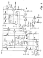
- FIGURE 2 is a schematic diagram of a gain-controlled amplifier stage that embodies the invention in one of its aspects and that is particularly well-suited for use as the output stage of a plural-stage IF amplifier.
- FIGURE 3 is a schematic diagram of a two-stage IF amplifier that embodies the invention in one of its aspects and that employs the gain-controlled amplifier stages of FIGURES 1 and 2 as its input stage and as its output stage, respectively,
- FIGURE 4 is a block schematic diagram of those portions of a television receiver or video tape recorder used for recovering audio-signal, video-signal and synchronizing-signal portions of a transmitted television signal, which television receiver uses intermediate-frequency amplifiers of the type shown in FIGURE 3.
- FIGURE 5 is a schematic diagram of a modification that can be made to the FIGURE 1 gain-controlled amplifier stage in an alternative embodiment of the invention.
- Q1 is a bipolar transistor having a base electrode for controlling conduction through a principal conduction path between emitter and collector electrodes, as is also the case with other bipolar transistors to be hereinafter referred to in the description.
- Transistor Q1 is of NPN conductivity type and has its base and collector electrodes conductively joined so as to operate in a diode-connected mode.
- the emitter electrode of Q1 connects to a source of a reference potential, here shown as ground.
- a reference current is supplied to the joined base and collector electrodes via a resistance R1 having one end thereof connected to those joined electrodes and having another end thereof connected to receive an automatic-gain-control (AGC) signal potential applied at a terminal T1.
- AGC automatic-gain-control
- FIGURE 1 shows the AGC signal potential originating from a generator GC1 being applied at a terminal T1.
- NPN transistors Q2 and Q3 have their respective emitter electrodes connected to the same reference potential as the emitter electrode of Q1 and their base electrodes connected to the base electrode of Q1, so as to form a current mirror arrangement with respect to the reference current supplied via R1.
- the emitter electrodes of NPN transistors Q4 and Q5 are each connected to one end of respective resistances R5 and R6 whose other ends are connected together and are connected to a point at ground reference potential via a series resistance R7, so that transistors Q4 and Q5 form a differential pair, with resistance R7 supplying operating current or tail current to the differential pair.
- NPN transistors Q6 and Q7 are connected to respective signal input terminals T5 and T6 for receiving a differential input signal and accompanying direct bias potential thereat.
- Figure 1 shows a battery B1 with its negative terminal connected to a point of ground reference potential supplying a positive direct bias potential V at its positive terminal against which are referred balanced input signals supplied by generators S1 and S2 to the base electrodes of Q6 and Q7.
- Transistors Q6 and Q7 are connected as common-collector amplifiers to provide voltage followers of the emitter follower type. Their respective emitter electrodes connect to respective ones of the base electrodes of Q4 and Q5 and to one end of respective resistances R2 and R3.
- Transistors Q6 and Q7 have their collector electrodes connected to receive a positive operating potential V B2 applied to a supply terminal T2, shown in FIGURE 1 as being supplied from the positive terminal of a battery B2 having its negative terminal connected to a point at reference ground potential.
- the collector electrodes of Q4 and Q5 are connected to supply terminal T2 via respective series resistances R8 and R9.
- the collector electrode of Q4 is further connected to the base electrode of an NPN transistor Q8, the collector electrode of which connects to T2.
- the emitter electrode of Q8 is connected to an output terminal T3 and is further connected to ground reference potential via a series resistance R10.
- the collector electrode of transistor Q5 is further connected to the base electrode of an NPN transistor Q9, the collector electrode of which connects to T2.
- the emitter electrode of Q9 is connected to an output terminal T4 and is further connected to ground reference potential via a series resistance R11.
- the collector electrode of transistor Q4 is further connected to the joined collector and base electrodes of an NPN transistor Q10 and to the emitter electrode of an NPN transistor Q11.
- the collector electrode of transistor Q5 is further connected to the joined collector and base electrodes of an NPN transistor Q12 and to the emitter electrode of an NPN transistor Q13.
- the joined emitter electrodes of transistors Q10 and Q12 are connected to the collector electrode of transistor Q3 via a series resistance R12.
- the joined collector and base electrodes of transistors Q11 and Q13 are connected to the collector electrode of a PNP transistor Q14, the emitter electrode of which is connected to supply terminal T2 via a series resistance R13.
- the base electrode of transistor Q14 is connected to the collector electrode of Q2 and is further connected via a series resistance R14 to the base and collector electrodes of a PNP transistor Q15.
- the emitter electrode of diode-connected transistor Q15 is connected to supply terminal T2.
- diode-connected transistors Q10, Q11, Q12 and Q13 in conjunction with resistors R8 and R9, form a variable load for the collector electrodes of the emitter-coupled differential amplifier transistors Q4 and Q5.
- the output signal is buffered by Q8 and Q9 operating as voltage followers of the emitter-follower type.
- the DC through diode-connected transistors Q10, Q11, Q12, and Q13 is determined by the current mirror output current in the collector electrode of Q3 and in the equal collector current of Q2, as thereafter mirrored by the current mirror formed by PNP transistors Q14 and Q15.
- diode-connected transistors Q10, Q11, Q12 and Q13 present high impedances. consequently, the amplifier gain as determined by the gain of the differential pari amplifier is at a maximum, being defined by the collector resistors.
- diode-connected transistors Q10, Q11, Q12 and Q13, and the transistors supplying current to them are well matched, there will be no disturbance of the DC conditions of operation of the amplifier as the gain is changed and thereby the problems referred to in connection with prior art arrangements are avoided and cascading of stages is facilitated. Such matching is readily accomplished on a monolithic IC.
- the network comprising diode-connected transistors Q10, Q11, Q12 and Q13 is in the form of a bridge, so that the nodes where currents are supplied to the network are at AC ground, forming a "virtual ground" for RF currents.
- the PNP transistor Q14 carries only DC and its collector capacitance does not affect the frequency response of the amplifier. Another effect is that there is no signal return to ground through the diode-connected transistors Q10, Q11, Q12 and Q13.
- the gain control variable elements are in the collector circuit of the differential pair amplifier, thereby allowing design freedom in biasing the emitter circuit for large signal handling capability and so extending the overload characteristic. Furthermore, the power require to effect gain control is limited.
- the collector loads of the emitter-coupled differential amplifier are just the resistive loads at maximum gain, since the diodes used to shunt them are nonconducting under this condition.
- the use of resistances as collector loads is advantageous in that: the maximum voltage gain of each stage can be predicted, despite the constructions of the gain-controlled amplifier in an IC, and this permits gain-controlled amplifier stages embodying the invention to be mass-produced in IC form without the need for individual adjustment of each amplifier stage in regard to maximum voltage gain.
- the maximum voltage gain of each amplifier stage is the product of the transconductance (g m ) of an emitter-coupled differential-amplifier transistor times the resistance (R L ) of its collector load.
- the g m of the transistor is determined by its emitter current flow, which current flow is made proportional to an applied bias voltage V BIAS (less, typically, a semiconductor junction offset voltage V BE ) applied across a resistive element with resistance R BIAS included on the IC with the resistive loads and arranged to be of the same type as the resistive loads.
- V BIAS a semiconductor junction offset voltage V BE
- V BE The few millivolt variation of V BE with temperature is usually negligible compared to (V BIAS - V BE ), a voltage which depends on the bias voltage V BIAS applied from off-chip and can be arranged to have a well-predicted value.
- the value of R L is normally chosen to provide a maximum voltage gain of about twenty times for a controlled-gain amplifier stage.
- the first stage of a PIX IF amplifier has to accommodate the full dynamic range of differential IF input potential signal to the amplifier, the amplitude of the IF signal supplied to the later stage(s) of the PIX IF amplifier being subject to a lesser dynamic range of input signal level owing to the gain control afforded by the first stage.
- the first stage of a PIX IF amplifier has to have the capability of avoiding overload on the peaks of the largest differential IF input signals received during strong-signal reception, when the gain control of the preceding RF amplifier runs out of range.
- the FIGURE 1 gain-controlled amplifier is fitted for use as the first stage of a PIX IF amplifier, with the differential amplifier transistors Q4 and Q5 being emitter-coupled with substantial differential-mode resistance between their emitter electrodes.
- the linear differential-mode resistance provided by the resistors R5 and R6 permits the differential IF input signal potential between their base electrodes to reach as high about 100 millivolts RMS without either transistor being cut off on signal peaks.
- the differential-mode resistance between the emitter electrodes of transistors Q4 and Q5 can be provided in other known ways -- e.g., by the resistance of the resistors R61 in the FIGURE 5 pi network replacement for the FIGURE 1 tee network connection of resistors R5, R6 and R7; by the resistance of a resistor corresponding to resistor R61 in another pi network that is a modification of the FIGURE 5 pi network, in which other pi network transistors biased for constant-current-source operation replace the resistors R62 and R63; and by the combined resistances of the resistors R5 and R6 in a modification of the FIGURE 1 tee network connection of resistors R5, R6 and R7 in which a transistor biased for constant-current-source operation replaces the resistor R7.
- a transistor Q21 is of NPN conductivity type and has its base and collector electrodes conductively joined so as to operate in a diode-connected mode.
- the emitter electrode of Q21 is connected via a series resistance R21 to a source of a reference potential, here shown as ground.
- a reference current is supplied to the joined base and collector electrodes via a resistance R22 having one end thereof connected thereto and another end thereof connected to receive a positive direct bias potential V B3 applied to a terminal T21.
- FIGURE 2 shows V B3 as being supplied from a battery B3.
- NPN transistor Q22 has its emitter electrode connected to ground via a series resistance R23 and its base electrode connected to the base electrode of transistors Q21, so as to form a current mirror arrangement with respect to the reference current supplied via R22.
- NPN transistors Q23 and Q24 form a differential amplifier pair, having their respective emitter electrodes connected to the collector electrode of transistor Q22.
- the base electrode of transistor Q23 is connected to a terminal T22 for receiving a gain control signal thereat, herein represented as being supplied by a source GC2, and the base electrode of transistor Q24 is connected to a termianl T23 for receiving a positive direct bias potential V B4 thereat, herein represented as being supplied by a battery B4.
- NPN transistors Q25 and Q26 form a differential amplifier pair wherein their emitter electrodes are connected to the collector electrode of transistor Q24. Their base electrodes are connected to respective input terminals T25 and T26 for receiving a balanced input signal referred to a direct bias potential.
- Figure 2 shows a battery BS with its negative terminal connected to a point of ground reference potential supplying a direct bias potential V B5 at its positive terminal against which are referred balanced input signals supplied by generators S3 and S4 to the terminals T25 and T26.
- the collector electrodes of transistors Q25 and Q26 are coupled via respective resistances R24 and R25 to a supply terminal T27 for receiving a positive operating potential V B2 , shown as being supplied from the battery B2.
- the collector electrode of transistor Q25 is further coupled to the joined collector and base electrodes of an NPN transistor Q27 and the collector electrode of transistor Q26 is further coupled to the joined collector and base electrodes of an NPN transistor Q28.
- the joined emitter electrodes of Q27 and Q28 are connected to the collector electrode of transistor Q23 and are further connected to terminal T27 by a resistance R26.
- NPN transistors Q29 and Q30 are arranged as voltage followers of the emitter-follower type, which serve as output buffer stages.
- the base electrodes of Q29 and Q30 connect to the collector electrodes of Q26 and Q25, respectively, and the collector electrodes of Q29 and Q30 connect to supply terminal T27.
- the emitter electrode of transistor Q29 is connected to an output signal terminal T28 and to one end of a resistance R28 the other end of which is connected to ground.
- the emitter electrode of transistor Q30 is connected to an output signal terminal T29 and to one end of a resistance R28 the other end of which is connected to ground.
- current from the current mirror output at the collector electrode of transistors Q22 is steered by the transistor pair Q23 and Q24, between providing tail current for the differential-amplifier transistors Q25 and Q26 on the one hand, and providing bias current for diode-connected transistors Q27 and Q28, on the other hand.
- the diode-connected transistors Q27 and Q28 carry no current, the gain is at its maximum value, being determined by maximum tail current and by the collector load resistances R24 and R25.
- the AGC potential GC2 is made positive enough to bias transistor Q23 into conduction, the diode-connected transistors Q27 and Q28 are biased into conduction to shunt the collector resistances R24 and R25 of the transistors Q25 and Q26 to reduce their gain.
- transistor Q23 reduces the current available for flow through Q24 and as tail current for the transistors Q25 and Q26, which reduced tail current operates them at reduce transconductance and thus reduces their gain further.
- the DC through each of resistances R24 and R25 is not disturbed by the operation of gain control.
- noise performance will start to degrade. This is because of the poorer noise figures of the transistors Q25 and Q26 as their internal emitter resistances increase responsive to reduced current conduction by the principal conduction path of transistor Q24.
- the reduction of stage gain by the shunting of the collector load resistances R24 and R25 by diode-connected transistors Q27 and Q28 is the mechanism for gain reduction principally relied on, rather than reduction of the transconductances of Q25 and Q26 through starvation of their tail current.
- the normal range of gain control is upward from about 0 dB, then, to 26 dB or so.
- the FIGURE 2 gain-controlled amplifier is not particularly well-suited for use as the initial stage of a plural-stage IF amplifier, because it will overload rather quickly on overlarge input signals. Since the FIGURE 2 gain-controlled amplifier relies more on diode shunting of the collector loads of the emitter-coupled transistors Q25 and Q26 than on reduction of their transconductances through starvation of their tail current, this shortcoming can be appreciably overcome by including emitter degeneration resistances for the transistors Q25 and Q26 in their emitter coupling.
- the modified stage still does not perform quite so well as the first stage of an IF amplifier as does the FIGURE 1 gain-controlled amplifier, because of the above-noted problem of noise figure being degraded as gain is cut back below 0 dB. In the later stage(s) of an IF amplifier, however, where the dynamic range of input signal to the stage(s) is reduced, the simpler construction of the FIGURE 2 gain-controlled amplifier makes it the favoured choice over the FIGURE 1 gain-controlled amplifier.
- FIGURE 3 shows a cascade connection of the FIGURE 1 and FIGURE 2 gain-controlled amplifiers.
- the two gain control signals at inputs T1 and at T22, respectively are arranged to cooperate such that, when gain reduction starts to be applied, the gain of the second amplifier is first reduced without reducing the gain of the first amplifier.
- the gain of the second amplifier has been reduced by a predetermined amount, subsequent amounts of gain reduction reduce the gain of both first and second amplifiers in a predetermined relationship.
- the first amplifier stage continues to operate at its full gain while overall gain reduction is achieved by reducing the gain of the second amplifier.
- delayed gain control is beneficial to the overall noise performance because the contribution of the second amplifier is thereby kept small for smaller signals where amplifier noise may still be significant.
- a delay is readily achievable by various means not shown here such as, for example, by the introduction of a voltage delay for the signal to the first amplifier.
- FIGURE 1 and FIGURE 2 amplifiers are suited for operation from a single positive operating supply, and FIGURE 3 accordingly shows the supply terminal T27 connecting from the supply terminal T2.
- the batteries B3 and B4 are replaced by networks within the same IC as the first and second gain-controlled amplifiers, which networks are of known type for deriving bias potentials from an operating supply potential as supplied via the supply terminal T2.
- FIGURE 4 shows those portions of a television receiver or video tape recorder used for recovering audio-signal, video-signal and synchronizing-signal portions of a transmitted television signal, which television receiver uses intermediate-frequency amplifiers of the type shown in FIGURE 3.
- FIGURE 4 is useful in understanding how delayed automatic gain control can be applied to intermediate-frequency amplifiers of the type shown in FIGURE 3.
- a down converter 14 which typically includes one or more tunable oscillators oscillating at frequencies above those in the television signal bands, responds to the amplified television signal supplied from the radio-frequency amplifier 12 to generate IF signals with sound carrier at 41.25 MHz and picture carrier at 45.75 MHz.
- IF signals are supplied to a block filter 16 that separates the sound carrier and its FM sidebands as well as the picture carrier, for application to a cascade connection of a first sound IF stage 18 and a second sound IF stage 20; and these IF signals are also supplied to a block filter 22 of relatively wide bandwidth that separates the vestigial picture carrier and its AM sideband for application to a cascade connection of a first picture IF stage 24 and a second picture IF stage 26.
- a second converter 28 of intercarrier type receives amplified IF signals from the second sound IF stage 20 and responds to generate a frequency-modulated 4.5 MHz intercarrier sound intermediate frequency selected by a bandpass filter 30 with a passband centered at 4.5 MHz.
- the bandpass filter 30 suppresses the image frequencies that would otherwise accompany the frequency-modulated 4.5 MHz intercarrier sound intermediate frequency, as applied to a limiter 32.
- the limiter 32 suppresses unwanted amplitude modulation of the frequency-modulated 4.5 MHz carrier it supplies as sound intermediate frequency response to an FM sound discriminator 34, which discriminator detects the frequency-modulation of the 4.5MHz carrier to generate the audio signal to be supplied to the remainder of the television receiver or video tape recorder.
- a sound overload detector 36 responds to the amplified IF signals from the second sound IF stage 20 exceeding a level acceptable as input signal to the down converter 28, to provide an auxiliary automatic-gain-control (AGC) signal to the first sound IF stage 18, augmenting during abnormal conditions a normal automatic-gain-control (AGC) signal generated responsive to PIX IF signal. Under normal conditions, however, both the sound IF and the PIX IF chains are gain controlled responsive solely to the normal automatic-gain control (AGG) signal generated responsive to PIX IF signal. To facilitate the AGC tracking between the sound IF and the PIX IF chains, the sound IF amplifiers 18 and 20 are constricted within the confines of the same IC as the PIX IF amplifiers 24 and 26.
- the down-converter 28, the overload detector 36, a video detector 38, an AGC detector 40 and AGC delay circuits 42 and 44 are advantageously included within the same IC as well.
- the video detector 38 which receives amplified IF signals from the second picture IF stage 26, detects a composite video signal.
- the automatic gain-control (AGC) detector 40 develops an automatic-gain-control (AGC) signal by detecting peaks of the synchronizing pulses included in the composite video signal.
- the AGC detector 40 is normally a keyed AGC detector in order to provide the AGC immunity to impulse noise.
- the video detector 38 is a synchronous detector, which is the modern trend in TV receiver design, the AGC detector 40 preferably includes filtering of its input signal to suppress response to the 2 MHz or so component of the composite video signal detected by the video detector 38, which component arises from the ringing of the block filter 22 at its midband natural frequency.
- This filtering of the input signal of the AGC detector 40 should pass frequencies up to about 500 Khz; this is so that equalizing pulses can be peak detected and the very top of the video image is not undesirably increased in brightness respective to the remainder of the video image.
- the AGC detector 40 in any case includes filtering of its output signal to a noise bandwidth of 400 Hz or so.
- the AGC signal developed by the AGC detector 40 proceeding from the composite video signal detected by the video detector 38 is used to control gain in both the PIX IF and the sound IF amplifiers as well as gain in the RF amplifier 12.
- Developing AGG proceeding from the composite video signal permits precise gain control of the PIX IF amplifiers, which have to amplify AM sidebands linearly.
- the sound IF amplifiers need only to amplify FM sidebands without too much gain to overload the down-converter 28, gross overloading of which is forestalled in any case by the sound overload detector 36.
- the bandpass filter 30 and the limiter 32 suppress the effects of any gain errors in the sound IF amplifier chain and the down-converter 28 as well.
- the AGC signal developed by the AGC detector 40 is applied in parallel, without delay, to the second stages 20 and 26 of the sound and PIX IF amplifiers.
- the AGG signal developed by the AGC detector 40 is applied in parallel, with delay, to the first stages 18 and 24 of the sound and PIX IF amplifiers.
- the first stages 18 and 24 of the sound and PIX IF amplifiers have delayed AGC applied to them via respective AGC delay circuits 42 and 44, so that only a single AGC line has to be run from the portion of the IC having the PIX IF located therein and the portion of the IC having the sound IF located therein.
- the AGC signal developed by the AGC detector 40 is applied to the RF amplifier 12 with still further delay, as provided by tuner gain control delay circuitry 46 usually located on the IF amplifier integrated-circuit chip. Under weak-signal-reception conditions. any reduction of the gain through the RF and IF amplifier chains takes place in the second stages 20 and 26 of the sound and PIX IF amplifiers.
- the RF amplifier 12 and the first stages 18 and 24 of the sound and PIX IF amplifiers operate at full gain to secure best signal-to-noise ratios in the signals supplied to the second stages 20 and 26 of the sound and PIX IF amplifiers.
- the AGC delay circuits 42 and 44 apply delayed AGC to the first stages 18 and 24 of the sound and PIX IF amplifiers to reduce their gain.
- the tuner gain control delay circuitry 46 applies AGC signal to the RF amplifier 12 to reduce its gain, thereby to avoid overloading the down-converter 14 and the first stages 18 and 24 of the sound and PIX IF amplifiers.
- the PIX IF chain is operated with balanced signals throughout, from the input signal applied to the first IF amplifier stage 24 from the PIX IF block filter 22 to the output from the second IF amplifier stage 26 to the video detector 28, in order to reduce self-oscillatory tendencies in the higher-gain portions of the PIX IF gain control range.
- the sound IF is operated with single-ended input signal applied to the first IF amplifier stage 18 from the sound IF block filter 16, allowing some simplification of that block filter 16, but the rest of the sound IF chain is operated with balanced signals, in order to reduce self-oscillatory tendencies in the higher-gain portions of the sound IF gain control range.
- the gain-controlled amplifier of FIGURE 2 may be readily modified so that gain reduction is effected in increasing degree by an AGC voltage becoming increasingly negative, rather than by an AGC voltage becoming increasingly positive.
- terminal T22 rather than terminal T23 is connected to receive a direct bias potential V B4 , and terminal T23 receives the AGC voltage that becomes increasingly negative so that gain reduction is effected in increasing degree.
- the gain-controlled amplifier of FIGURE 1 can also be modified so that gain reduction is effected in increasing degree by an AGC voltage becoming increasingly negative.
- One way to do this is to replace the current source and sink together comprising elements R1, Q2, Q3, R13, R14, Q14 and Q15 with: a single-output current mirror for sinking via the resistor R12 the combined emitter currents of Q10 and Q12 an output current scaled to an input current supplied to that current mirror; a dual-output current mirror having an input connection referred in potential to V B2 , having a first output connection for supplying the input current of the single-input current mirror, and having a second output connection for providing a current equal to the output current of the single-input current mirror as a source current to the combined base and collector currents of Q11 and Q13; and a resistor connected between terminal T1 and the input connection of the dual-output current mirror to generate an input current to that current mirror directly related to the AGC potential applied to terminal T1.
- FIGURE 5 shows a modification that can be made to the FIGURE 1 gain-controlled amplifier, in which modification the tee connection of resistors R5, R6 and R7 is replaced by an equivalent pi connection of resistors R61, R62 and R63.
- the resistance of R51 equals the sum of the resistances of R5 and R6; the resistance of R62 equals the sum of the resistances of R5 and R7; the resistance of R63 equals the sum of the resistances of R6 and R7.
- FIGURE 5 shows a modification that can be made to the FIGURE 1 gain-controlled amplifier, in which modification the tee connection of resistors R44, R45 and the constant current source formed by transistor Q42 and resistor R43 is replaced by an equivalent pi connection of resistor R64 and two constant current sources, one formed by transistor Q61 and resistor R65, and the other formed by transistor Q62 and resistor R66. That is, the single-output current mirror comprising elements Q41, R41, Q42 and R43 is replaced by a dual-output current mirror comprising elements Q41, R41, Q61, R65, Q62 and R66.
- the present invention is herein disclosed and its principles explained by way of exemplary embodiments. However, the invention is by no means limited to such embodiments, as will be apparent to one skilled in the art. Various changes and modifications can be incorporated.
- the embodiments herein described utilize NPN amplifying transistors; clearly, PNP transistors can be substituted with appropriate circuit modifications as familiar to persons skilled in the art, or field effect transistors may be used instead of bipolar transistors, again with appropriate circuit modifications as are familiar to persons skilled in the art.
- other forms of current mirrors can replace the particular forms herein used by way of explanation.
Landscapes
- Engineering & Computer Science (AREA)
- Multimedia (AREA)
- Signal Processing (AREA)
- Control Of Amplification And Gain Control (AREA)
- Amplifiers (AREA)
- Television Receiver Circuits (AREA)
Claims (7)
- Amplificateur à commande de gain comprenant :un premier et un second transistors (Q4, Q5) connectés sous la forme d'un premier amplificateur différentiel à liaison par les émetteurs, les premier et second transistors (Q4, Q5) recevant sur leurs électrodes de base respectives une tension de polarisation directe de base (Vm), l'amplificateur différentiel étant disposé de manière à répondre à des signaux d'entrée HF (S1, S2) appliqués entre les électrodes de base desdits premier et second transistors (Q4, Q5) et disposant d'électrodes respectives de collecteur destinées à générer des courants de collecteur respectifs présentant des composantes continues en mode commun respectives et des composantes HF en mode différentiel respectives, l'amplificateur étant caractérisé en ce que des moyens de charge de diodes connectées en pont (Q10, Q13) sont prévus, avec des première, seconde, troisième et quatrième connexions, lesdites première et seconde connexions étant équilibrées relativement auxdites troisième et quatrième connexions, lesdites première et seconde connexions étant raccordées auxdites électrodes de collecteur respectives, lesdits moyens de charge de diode (Q10, Q13) présentant entre lesdites première et seconde connexions une impédance pouvant être commandée présentant une valeur contrôlée par un flux de courant entre lesdites troisième et quatrième connexions, et des moyens de courant variable de commande sont prévus comprenant une sortie génératrice de courant (Q14) connectée à ladite troisième connexion et une sortie réceptrice de courant (Q3) connectée à ladite quatrième connexion, lesdites sorties génératrice et réceptrice de courant produisant des amplitudes de courant égales.
- Etage d'amplificateur à commande de gain selon la revendication 1, dans lequel lesdits moyens de charge de diodes connectées en pont comprennent une première paire de diodes (Q11, Q13) ayant leurs anodes respectives raccordées à ladite troisième connexion et ayant leurs cathodes respectives raccordées auxdites première et seconde connexions respectivement et une seconde paire de diodes (Q10, Q12) ayant leurs cathodes respectives raccordées à ladite quatrième connexion et ayant leurs anodes respectives raccordées auxdites première et seconde connexions respectivement.
- Etage d'amplificateur à commande de gain selon la revendication 1 ou 2, dans lequel est prévu :une première et une seconde résistances (R8, R9) ayant leurs premières extrémités respectives raccordées aux électrodes respectives de collecteur desdits premier et second transistors (Q4, Q5) et leurs secondes extrémités respectives raccordées à une borne (T2) afin de recevoir une tension de commande directe (VB2).
- Etage d'amplificateur à commande de gain selon la revendication 3, dans lequel ladite source de courant (Q14) présente une valeur d'impédance de source appartenant à un intervalle de valeurs à progression ascendante à partir d'une valeur comparable à l'impédance desdites première et seconde résistances (R8, R9).
- Amplificateur selon l'une quelconque des revendications précédentes, dans lequel ledit récepteur de courant (Q3) présente une valeur d'impédance de source appartenant à un intervalle de valeurs progressant à partir d'une première valeur comparable à l'impédance desdites première et seconde résistances (R8, R9) jusqu'à une seconde valeur comparativement élevée par comparaison à celle-ci.
- Amplificateur à commande de gain à deux étages ayant un premier étage comprenant un amplificateur à commande de gain conforme à l'une quelconque des revendications 1 à 5 et un second étage comprenant :des troisième et quatrième transistors (Q25, Q26) ayant des électrodes respectives de base, d'émetteur et de collecteur ;des moyens de connexion dudit troisième transistor et dudit quatrième transistor (Q25, Q26) dans une seconde configuration d'amplificateur différentiel à liaison par les émetteurs, afin que lesdits troisième et quatrième transistors (Q25, Q26) produisent à partir de leurs électrodes de collecteur respectives des courants de collecteur respectifs présentant des composantes continues en mode commun respectives et présentant des composantes HF en mode différentiel respectives en réaction aux signaux HF reçus entre leurs électrodes de base ;un premier diviseur de courant pouvant être commandé (Q23, Q24) présentant une entrée destinée à conduire un courant d'activation direct, ayant une première et une seconde sorties reliées afin de permettre l'application des première et seconde parties fractionnées dudit courant d'activation direct à diviser en une première et une seconde parties fractionnées selon un rapport déterminé en fonction d'un premier signal de commande (GC2), aux dites électrodes d'émetteur desdits troisième et quatrième transistors (Q25, Q26) respectivement ;une troisième résistance (R24) raccordée entre ladite électrode de collecteur dudit troisième transistor (Q25) et un point de potentiel de fonctionnement (T27) ;une quatrième résistance (R25) raccordée entre ladite électrode de collecteur dudit quatrième transistor (Q26) et ledit point de potentiel de fonctionnement (T27) ;un premier moyen diode (Q27) ayant une première électrode à laquelle est reliée ladite électrode de collecteur dudit troisième transistor (Q25) et ayant une seconde électrode ;un second moyen diode (Q28) ayant une première électrode à laquelle est reliée ladite électrode de collecteur dudit quatrième transistor (Q26) et ayant une seconde électrode ; etune interconnexion entre lesdites secondes électrodes desdits premier et second moyens diode (Q27, Q28) auxquels ladite seconde sortie dudit premier diviseur de courant (Q23, Q24) est reliée.
- Récepteur de télévision comportant un amplificateur à commande de gain conforme à l'une quelconque des revendications 1 à 5 ou comportant un amplificateur à deux étages conforme à la revendication 6.
Applications Claiming Priority (3)
| Application Number | Priority Date | Filing Date | Title |
|---|---|---|---|
| US07/940,220 US5331290A (en) | 1992-09-08 | 1992-09-08 | Variable gain amplifier |
| US940220 | 1992-09-08 | ||
| PCT/KR1993/000018 WO1994006244A1 (fr) | 1992-09-08 | 1993-03-10 | Amplificateur a gain variable |
Publications (2)
| Publication Number | Publication Date |
|---|---|
| EP0611509A1 EP0611509A1 (fr) | 1994-08-24 |
| EP0611509B1 true EP0611509B1 (fr) | 1998-05-20 |
Family
ID=25474440
Family Applications (1)
| Application Number | Title | Priority Date | Filing Date |
|---|---|---|---|
| EP93905645A Expired - Lifetime EP0611509B1 (fr) | 1992-09-08 | 1993-03-10 | Amplificateur a gain variable |
Country Status (8)
| Country | Link |
|---|---|
| US (1) | US5331290A (fr) |
| EP (1) | EP0611509B1 (fr) |
| JP (1) | JP3263395B2 (fr) |
| KR (1) | KR0157485B1 (fr) |
| CN (1) | CN1082313C (fr) |
| DE (1) | DE69318694T2 (fr) |
| RU (1) | RU2140705C1 (fr) |
| WO (1) | WO1994006244A1 (fr) |
Families Citing this family (29)
| Publication number | Priority date | Publication date | Assignee | Title |
|---|---|---|---|---|
| US5764106A (en) * | 1993-12-09 | 1998-06-09 | Northern Telecom Limited | Gain-controlled amplifier and automatic gain control amplifier using GCLBT |
| KR0151414B1 (ko) * | 1993-12-30 | 1998-10-15 | 김광호 | 영상처리 시스템의 자동이득 조절회로 |
| US5448311A (en) * | 1994-08-22 | 1995-09-05 | Thomson Consumer Electronics, Inc. | Tri-state video differential driver |
| US5530403A (en) * | 1995-05-03 | 1996-06-25 | Motorola, Inc. | Low-voltage differential amplifier |
| US6445425B1 (en) * | 1997-01-07 | 2002-09-03 | Samsung Electronics Co., Ltd. | Automatic fine tuning of receiver for digital television signals |
| US6046781A (en) * | 1997-01-07 | 2000-04-04 | Samsung Electronics Co., Ltd. | Automatic fine tuning of TV receiver for receiving both digital and analog TV signals |
| US5990740A (en) * | 1997-12-02 | 1999-11-23 | Nokia Mobile Phones | Differential amplifier with adjustable linearity |
| DE19916902B4 (de) * | 1999-04-14 | 2015-08-20 | Siemens Aktiengesellschaft | Verstärkereinrichtung mit veränderbarer Arbeitspunkteinstellung sowie Verwendung der Verstärkereinrichtung |
| SG92689A1 (en) | 2000-03-27 | 2002-11-19 | Koninkl Philips Electronics Nv | Automatic gain control |
| US6392487B1 (en) | 2000-08-02 | 2002-05-21 | Rf Micro Devices, Inc | Variable gain amplifier |
| US6404283B1 (en) * | 2000-08-18 | 2002-06-11 | Motorola, Inc. | Method and apparatus for amplifying a radio frequency signal |
| JP4265865B2 (ja) * | 2000-09-14 | 2009-05-20 | 富士通マイクロエレクトロニクス株式会社 | 能動負荷回路 |
| CA2329294C (fr) * | 2000-12-21 | 2007-01-02 | Pulp And Paper Research Institute Of Canada | Methode et appareil de mesure de proprietes de fibres |
| JP4405113B2 (ja) * | 2001-08-16 | 2010-01-27 | パナソニック株式会社 | 利得可変増幅回路 |
| JP3878625B2 (ja) * | 2003-06-20 | 2007-02-07 | 松下電器産業株式会社 | 振幅調整回路、モータ駆動制御装置、振幅調整方法、及びモータ駆動制御方法 |
| JP2008514089A (ja) | 2004-09-16 | 2008-05-01 | コーニンクレッカ フィリップス エレクトロニクス エヌ ヴィ | 信号スプリッタ |
| US7119618B2 (en) * | 2004-12-13 | 2006-10-10 | Semiconductor Components Industries, L.L.C. | Method of forming a wide bandwidth differential amplifier and structure therefor |
| WO2009070937A1 (fr) * | 2007-11-26 | 2009-06-11 | Hong Kong Applied Science and Technology Research Institute Co. Ltd | Circuit de commande de gain |
| US7679431B2 (en) * | 2007-11-26 | 2010-03-16 | Broadcom Corporation | Low flicker noise mixer and buffer |
| US8582035B2 (en) * | 2011-02-22 | 2013-11-12 | Intel Corporation | Apparatus, systems and methods utilizing adjacent-channel power dependent automatic gain control for digital television demodulation |
| JP5917858B2 (ja) * | 2011-08-29 | 2016-05-18 | ルネサスエレクトロニクス株式会社 | 半導体集積回路装置 |
| CN102364875B (zh) * | 2011-11-15 | 2016-01-13 | 南京美辰微电子有限公司 | 一种双环反馈高线性度可变增益放大器 |
| CN102571014B (zh) * | 2012-02-10 | 2014-03-12 | 中国科学院微电子研究所 | 一种电压型自动增益控制电路 |
| US9893693B2 (en) | 2012-12-07 | 2018-02-13 | Futurewei Technologies, Inc. | Gain control method for a broadband inductorless low noise amplifier |
| EA025687B1 (ru) * | 2014-02-06 | 2017-01-30 | Владимир Петрович Федосов | Выходной каскад усилителя мощности звуковой частоты |
| JP2016187080A (ja) * | 2015-03-27 | 2016-10-27 | 住友電気工業株式会社 | 利得可変差動増幅回路 |
| CN107181468B (zh) * | 2017-07-07 | 2024-09-24 | 曹银明 | 一种可变增益音频放大器 |
| RU2684510C1 (ru) * | 2018-04-16 | 2019-04-09 | Российская Федерация, от имени которой выступает Государственная корпорация по атомной энергии "Росатом" (Госкорпорация "Росатом") | Схема автоматической регулировки усиления электрических сигналов |
| US10700652B2 (en) | 2018-09-17 | 2020-06-30 | Texas Instruments Incorporated | Ethernet line driver |
Family Cites Families (22)
| Publication number | Priority date | Publication date | Assignee | Title |
|---|---|---|---|---|
| US464632A (en) * | 1891-12-08 | Egbert p | ||
| DE537202C (de) * | 1929-01-26 | 1931-10-31 | Radio Electr Soc Fr | Einrichtung zur Verringerung des Schwundes bei drahtloser Nachrichtenuebermittlung |
| US3241078A (en) * | 1963-06-18 | 1966-03-15 | Honeywell Inc | Dual output synchronous detector utilizing transistorized differential amplifiers |
| US3290520A (en) * | 1965-01-26 | 1966-12-06 | Rca Corp | Circuit for detecting amplitude threshold with means to keep threshold constant |
| US3522548A (en) * | 1968-05-03 | 1970-08-04 | Rca Corp | Temperature tracking of emitter coupled differential amplifier stage |
| NL6807207A (fr) * | 1968-05-22 | 1969-11-25 | ||
| US3541466A (en) * | 1969-01-07 | 1970-11-17 | Rca Corp | Gated differential amplifier |
| US3577008A (en) * | 1969-01-22 | 1971-05-04 | Rca Corp | Automatic frequency control apparatus |
| US3513256A (en) * | 1969-03-07 | 1970-05-19 | Sprague Electric Co | Synchronous demodulator for color television signals |
| US3707603A (en) * | 1969-12-29 | 1972-12-26 | Rca Corp | Fm stereophonic receiver detection apparatus and disabling means |
| US3651418A (en) * | 1970-11-16 | 1972-03-21 | Rca Corp | Synchronous detector control |
| JPS5625815B2 (fr) * | 1974-02-14 | 1981-06-15 | ||
| JPS5634409Y2 (fr) * | 1975-03-12 | 1981-08-14 | ||
| US4342005A (en) * | 1980-06-26 | 1982-07-27 | Rca Corporation | Television intermediate frequency amplifier with feedback stabilization |
| JPS5718109A (en) * | 1980-07-08 | 1982-01-29 | Toshiba Corp | Sound volume controlling circuit |
| DE3223229C2 (de) * | 1982-06-22 | 1986-11-13 | Texas Instruments Deutschland Gmbh, 8050 Freising | Hochfrequenzverstärker |
| JPH0787556B2 (ja) * | 1984-03-30 | 1995-09-20 | パイオニア株式会社 | テレビ受信機 |
| US4706285A (en) | 1985-12-24 | 1987-11-10 | Rca Corporation | Automatic gain control of a scrambled video signal |
| US4718086A (en) * | 1986-03-27 | 1988-01-05 | Rca Corporation | AGC in sound channel of system for processing a scrambled video signal |
| US4974087A (en) * | 1989-04-13 | 1990-11-27 | Rca Licensing Corporation | Parallel sound if with reference carrier derived from quasi-synchronous video detector |
| EP2580967A1 (fr) | 2011-10-11 | 2013-04-17 | Nestec S.A. | Accélération de récupération musculaire après une atrophie du muscle induite par l'immobilisation |
| WO2013059832A1 (fr) | 2011-10-21 | 2013-04-25 | Incube Labs, Llc | Appareil de mesure oxymétrique implantable et son procédé d'utilisation |
-
1992
- 1992-09-08 US US07/940,220 patent/US5331290A/en not_active Expired - Lifetime
-
1993
- 1993-03-10 WO PCT/KR1993/000018 patent/WO1994006244A1/fr not_active Ceased
- 1993-03-10 DE DE69318694T patent/DE69318694T2/de not_active Expired - Fee Related
- 1993-03-10 KR KR1019940700599A patent/KR0157485B1/ko not_active Expired - Fee Related
- 1993-03-10 EP EP93905645A patent/EP0611509B1/fr not_active Expired - Lifetime
- 1993-03-10 JP JP50663394A patent/JP3263395B2/ja not_active Expired - Fee Related
- 1993-03-10 RU RU93058627A patent/RU2140705C1/ru not_active IP Right Cessation
- 1993-03-20 CN CN93103149A patent/CN1082313C/zh not_active Expired - Fee Related
Also Published As
| Publication number | Publication date |
|---|---|
| JPH07500957A (ja) | 1995-01-26 |
| DE69318694D1 (de) | 1998-06-25 |
| CN1082313C (zh) | 2002-04-03 |
| KR0157485B1 (ko) | 1999-02-18 |
| RU2140705C1 (ru) | 1999-10-27 |
| WO1994006244A1 (fr) | 1994-03-17 |
| EP0611509A1 (fr) | 1994-08-24 |
| CN1083998A (zh) | 1994-03-16 |
| US5331290A (en) | 1994-07-19 |
| DE69318694T2 (de) | 1998-10-29 |
| JP3263395B2 (ja) | 2002-03-04 |
Similar Documents
| Publication | Publication Date | Title |
|---|---|---|
| US5331290A (en) | Variable gain amplifier | |
| US5365279A (en) | Using D-C feedback with on-chip filtering to balance I-F drive to second detector in monolithic IC | |
| EP0656164B1 (fr) | Récepteur de télévision | |
| US4417270A (en) | Wide band chrominance demodulator with color noise reduction function | |
| CA2126854C (fr) | Amplificateur video fi avec amplificateur fi auxiliaire pour son interporteur et syntonisation precise automatique | |
| US4399460A (en) | Video signal peaking control system with provision for automatic and manual control | |
| KR100211412B1 (ko) | Fm 라디오를 포함하는 텔레비젼 수상기 | |
| US5361406A (en) | Audio level equalization of broadcast and national weather service FM radio signals | |
| US4511924A (en) | Frequency translation phase-locked loop for separate or intercarrier type television sound detection | |
| EP1171998B1 (fr) | Appareil de traitement de signaux fi | |
| JPH06105967B2 (ja) | ビデオ信号処理装置における自動利得制御装置 | |
| US7202910B1 (en) | Signal processing apparatus | |
| JPS6247017B2 (fr) | ||
| CA1257380A (fr) | Dispositif de demodulation de signaux de chrominance | |
| CA1185355A (fr) | Dispositif de commande a selection de frequence et a couplage direct pour signaux video insensible aux composantes continues des signaux video | |
| US4388647A (en) | Predictably biased DC coupled video signal peaking control system | |
| EP1104183A2 (fr) | Dispositif récepteur et récepteur de télévision et appareil d'enregistrement et de reproduction utilisant le dispositif | |
| JPH06260954A (ja) | テレビ信号受信機 | |
| Brilka et al. | A new single-reference VIF/SIF/PLL for multistandard signal detection in TV sets and VCRs | |
| JPS6075133A (ja) | 自動利得制御方式 |
Legal Events
| Date | Code | Title | Description |
|---|---|---|---|
| PUAI | Public reference made under article 153(3) epc to a published international application that has entered the european phase |
Free format text: ORIGINAL CODE: 0009012 |
|
| 17P | Request for examination filed |
Effective date: 19940509 |
|
| AK | Designated contracting states |
Kind code of ref document: A1 Designated state(s): DE GB NL |
|
| 17Q | First examination report despatched |
Effective date: 19960530 |
|
| GRAG | Despatch of communication of intention to grant |
Free format text: ORIGINAL CODE: EPIDOS AGRA |
|
| GRAG | Despatch of communication of intention to grant |
Free format text: ORIGINAL CODE: EPIDOS AGRA |
|
| GRAH | Despatch of communication of intention to grant a patent |
Free format text: ORIGINAL CODE: EPIDOS IGRA |
|
| GRAH | Despatch of communication of intention to grant a patent |
Free format text: ORIGINAL CODE: EPIDOS IGRA |
|
| GRAA | (expected) grant |
Free format text: ORIGINAL CODE: 0009210 |
|
| AK | Designated contracting states |
Kind code of ref document: B1 Designated state(s): DE GB NL |
|
| REF | Corresponds to: |
Ref document number: 69318694 Country of ref document: DE Date of ref document: 19980625 |
|
| PLBE | No opposition filed within time limit |
Free format text: ORIGINAL CODE: 0009261 |
|
| STAA | Information on the status of an ep patent application or granted ep patent |
Free format text: STATUS: NO OPPOSITION FILED WITHIN TIME LIMIT |
|
| 26N | No opposition filed | ||
| REG | Reference to a national code |
Ref country code: GB Ref legal event code: IF02 |
|
| PGFP | Annual fee paid to national office [announced via postgrant information from national office to epo] |
Ref country code: NL Payment date: 20080303 Year of fee payment: 16 Ref country code: GB Payment date: 20080305 Year of fee payment: 16 |
|
| PGFP | Annual fee paid to national office [announced via postgrant information from national office to epo] |
Ref country code: DE Payment date: 20080306 Year of fee payment: 16 |
|
| GBPC | Gb: european patent ceased through non-payment of renewal fee |
Effective date: 20090310 |
|
| NLV4 | Nl: lapsed or anulled due to non-payment of the annual fee |
Effective date: 20091001 |
|
| PG25 | Lapsed in a contracting state [announced via postgrant information from national office to epo] |
Ref country code: DE Free format text: LAPSE BECAUSE OF NON-PAYMENT OF DUE FEES Effective date: 20091001 |
|
| PG25 | Lapsed in a contracting state [announced via postgrant information from national office to epo] |
Ref country code: NL Free format text: LAPSE BECAUSE OF NON-PAYMENT OF DUE FEES Effective date: 20091001 |
|
| PG25 | Lapsed in a contracting state [announced via postgrant information from national office to epo] |
Ref country code: GB Free format text: LAPSE BECAUSE OF NON-PAYMENT OF DUE FEES Effective date: 20090310 |