EP0613012B1 - Kapazitiver Beschleunigungsmesser mit Schaltung zur Korrektur des störender Einflusses parasitärer Kapazitäten - Google Patents
Kapazitiver Beschleunigungsmesser mit Schaltung zur Korrektur des störender Einflusses parasitärer Kapazitäten Download PDFInfo
- Publication number
- EP0613012B1 EP0613012B1 EP94410002A EP94410002A EP0613012B1 EP 0613012 B1 EP0613012 B1 EP 0613012B1 EP 94410002 A EP94410002 A EP 94410002A EP 94410002 A EP94410002 A EP 94410002A EP 0613012 B1 EP0613012 B1 EP 0613012B1
- Authority
- EP
- European Patent Office
- Prior art keywords
- voltage
- capacitors
- accelerometer
- voltages
- compensation
- Prior art date
- Legal status (The legal status is an assumption and is not a legal conclusion. Google has not performed a legal analysis and makes no representation as to the accuracy of the status listed.)
- Expired - Lifetime
Links
- 230000000694 effects Effects 0.000 title claims description 11
- 230000003071 parasitic effect Effects 0.000 title description 19
- 239000003990 capacitor Substances 0.000 claims description 52
- 230000005284 excitation Effects 0.000 claims description 35
- 238000005259 measurement Methods 0.000 claims description 28
- XUIMIQQOPSSXEZ-UHFFFAOYSA-N Silicon Chemical compound [Si] XUIMIQQOPSSXEZ-UHFFFAOYSA-N 0.000 claims description 13
- 230000001133 acceleration Effects 0.000 claims description 13
- 229910052710 silicon Inorganic materials 0.000 claims description 12
- 239000010703 silicon Substances 0.000 claims description 12
- 230000003068 static effect Effects 0.000 claims description 4
- VYPSYNLAJGMNEJ-UHFFFAOYSA-N Silicium dioxide Chemical compound O=[Si]=O VYPSYNLAJGMNEJ-UHFFFAOYSA-N 0.000 claims description 3
- 229910052814 silicon oxide Inorganic materials 0.000 claims description 3
- 230000001771 impaired effect Effects 0.000 claims 1
- 238000012545 processing Methods 0.000 description 13
- 238000012937 correction Methods 0.000 description 11
- 238000010586 diagram Methods 0.000 description 11
- 230000014509 gene expression Effects 0.000 description 7
- 235000012431 wafers Nutrition 0.000 description 6
- 238000006073 displacement reaction Methods 0.000 description 4
- 239000000243 solution Substances 0.000 description 4
- 230000001360 synchronised effect Effects 0.000 description 4
- 230000008901 benefit Effects 0.000 description 3
- 238000000034 method Methods 0.000 description 3
- 238000006243 chemical reaction Methods 0.000 description 2
- 239000003795 chemical substances by application Substances 0.000 description 2
- 238000010276 construction Methods 0.000 description 2
- 238000005516 engineering process Methods 0.000 description 2
- 238000002347 injection Methods 0.000 description 2
- 239000007924 injection Substances 0.000 description 2
- 230000000737 periodic effect Effects 0.000 description 2
- 230000010363 phase shift Effects 0.000 description 2
- 238000012360 testing method Methods 0.000 description 2
- 238000001514 detection method Methods 0.000 description 1
- 238000002474 experimental method Methods 0.000 description 1
- 238000002955 isolation Methods 0.000 description 1
- 230000007246 mechanism Effects 0.000 description 1
- 238000012986 modification Methods 0.000 description 1
- 230000004048 modification Effects 0.000 description 1
- 230000003472 neutralizing effect Effects 0.000 description 1
- 230000003287 optical effect Effects 0.000 description 1
- 244000045947 parasite Species 0.000 description 1
- 230000008569 process Effects 0.000 description 1
- 239000000725 suspension Substances 0.000 description 1
- 230000001131 transforming effect Effects 0.000 description 1
- 238000011144 upstream manufacturing Methods 0.000 description 1
Images



Classifications
-
- G—PHYSICS
- G01—MEASURING; TESTING
- G01P—MEASURING LINEAR OR ANGULAR SPEED, ACCELERATION, DECELERATION, OR SHOCK; INDICATING PRESENCE, ABSENCE, OR DIRECTION, OF MOVEMENT
- G01P15/00—Measuring acceleration; Measuring deceleration; Measuring shock, i.e. sudden change of acceleration
- G01P15/02—Measuring acceleration; Measuring deceleration; Measuring shock, i.e. sudden change of acceleration by making use of inertia forces using solid seismic masses
- G01P15/08—Measuring acceleration; Measuring deceleration; Measuring shock, i.e. sudden change of acceleration by making use of inertia forces using solid seismic masses with conversion into electric or magnetic values
- G01P15/13—Measuring acceleration; Measuring deceleration; Measuring shock, i.e. sudden change of acceleration by making use of inertia forces using solid seismic masses with conversion into electric or magnetic values by measuring the force required to restore a proofmass subjected to inertial forces to a null position
- G01P15/131—Measuring acceleration; Measuring deceleration; Measuring shock, i.e. sudden change of acceleration by making use of inertia forces using solid seismic masses with conversion into electric or magnetic values by measuring the force required to restore a proofmass subjected to inertial forces to a null position with electrostatic counterbalancing means
Definitions
- the present invention relates to accelerometers comprising a capacitive silicon acceleration detector, and a system for measuring the capacitive imbalance of the detector, providing an electrical signal representative of the acceleration.
- FIG. 1 A very schematic example of a capacitive silicon acceleration detector is illustrated by the sectional view of FIG. 1.
- the detector 1 comprises a central silicon wafer 2 sandwiched between two external silicon wafers 3,4.
- the central silicon wafer 2 is etched before assembly so as to include a frame 5 and a central plate, or movable mass 6, fixed to the frame 5 by one or more suspension arms 7.
- the isolation of the frame 5 from the central wafer vis-à-vis the external plates 3,4 is provided by insulating strips 8,9 generally made of silicon oxide.
- the external plates 3,4 define with the frame 5 a space within which the mobile mass 6 is suspended.
- the upper and lower faces of the mobile mass 6 as well as the faces of the plates 3,4 facing the mobile mass include conductive surfaces, or electrodes 10, 11, 12, 13, forming a system of two capacitors Cs, Ci symmetrical with respect to the median plane of the detector 1. Access to the electrodes 10 to 13 is achieved by means of contact pads and internal links, not shown in FIG. 1. Most often, the mobile electrodes 10, 11 are not isolated from the mobile mass 6 (these are then silicon doped zones) and are at the same electrical potential, so that only one contact pad is provided for these two electrodes.
- the mobile mass 6 moves, relative to its rest position, by an amount z proportional to the acceleration.
- the detector 1 described above is associated with a system for measuring the imbalance of the capacitors Cs, Ci.
- FIG. 2 represents the electrical diagram of a conventional accelerometer 20 comprising the detector 1 already described and such a measurement system.
- the detector 1 is represented by the two capacitors Cs, Ci formed by the electrodes 10,12 and 11,13, the pad common to the electrodes 10,11 being materialized by a node 14.
- the measurement system comprises an excitation stage 21 capacitors Cs, Ci, supplied by an alternating reference voltage v, a stage 30 for processing the signal from the detector, delivering a measurement voltage vs, and a feedback loop 26 bringing the voltage vs at the input of stage d excitement 21.
- the excitation stage 21 drives the fixed electrode 12 of the capacitor Cs by means of a differential amplifier 22, and the fixed electrode 13 of the capacitor Ci by means of an adder amplifier 23.
- the negative input of amplifier 22 and a first input of amplifier 23 are connected to an amplifier 24 of gain b, receiving as input the reference voltage v.
- the positive input of the amplifier 22 and the other input of the amplifier 23 are connected to the output of a gain amplifier 25 a, receiving as input the voltage vs delivered by the processing stage 30, brought to the stage of excitation by the feedback loop 26.
- the processing stage 30 essentially comprises a current / voltage converter 31 the input of which is connected to the node 14, followed by an amplifier 33 having a very high gain G, delivering the measurement voltage vs.
- the converter 31 is represented diagrammatically by an operational amplifier 32 whose output is brought back into input by a capacitor of capacity Cr.
- the voltage vs is used as the output voltage of the measurement system. It is rectified in a demodulator 40 connected to the output of the loop 26 and synchronized to the voltage v, which delivers a voltage Us constituting the output signal from the accelerometer.
- the excitation stage 21 applies on the fixed electrodes 12, 13 capacitors Cs, Ci excitation voltages having the respective expressions avs-bv and avs + bv .
- the input of the current / voltage converter 31 collects a differential current from the node 14 and due to the excitation of the capacitors Cs, Ci.
- an object of the present invention is to provide an accelerometer in which the disturbing effect of the parasitic capacitances on the linearity of the output signal is compensated.
- the present invention provides an accelerometer comprising a capacitive silicon detector forming a system of two variable capacitors whose capacitive imbalance is a function of the acceleration, the capacitors being disturbed by parasitic capacitances in parallel, an electronic system for measuring the capacitive imbalance of the detector, delivering an output voltage representative of the acceleration and comprising, an excitation stage, for applying to the capacitors excitation voltages developed by weighted combination of a reference voltage and the output voltage, a current / voltage converter stage, for collecting currents from each of the capacitors, delivering a measurement voltage, a feedback loop, for bringing the measurement voltage back to the excitation stage, the output voltage being taken at the output of the reaction loop, accelerometer comprising a stage for compensating for the disturbing effect of the parasitic capacitances, arranged to inject into the system measurement an electrical correction signal developed from the reference and measurement voltages and chosen so that the output voltage is substantially proportional to the ratio of the difference to the sum of the capacitors.
- the compensation stage injects into the reaction loop a correction voltage chosen so that the output voltage is equal to the weighted sum of the measurement and reference voltages, the weighting coefficients of the weighted sum being parameters for adjusting the compensation stage.
- the compensation stage comprises an operational amplifier arranged in series in the feedback loop and mounted as an adder, the output of the amplifier being brought back to its input by a first resistor, the measurement and reference voltages being brought to this same input via respectively a second and third resistance, the ratio of the first to the second resistance and the ratio of the first to the third resistance constituting the parameters for adjusting the compensation stage.
- the reference, measurement and output voltages can be periodic voltages, or direct voltages.
- the excitation stage comprises switches for cutting the excitation voltages applied to the capacitors
- the converter stage comprises a current / voltage converter followed by a demodulator.
- the compensation stage injects at the input of the converter stage a correction current adding to the currents collected from the capacitors, and chosen to cancel the current due to the excitation of the parasitic capacities.
- the correction current comes from two compensating capacitors excited by voltages respectively equal to the difference and to the sum of a voltage proportional to the reference voltage and a voltage proportional to the measurement voltage, the voltages excitation of the compensation capacitors constituting parameters for adjusting the compensation stage.
- the reference, output and measurement voltages are direct voltages, the excitation voltages of the detector capacitors and of the compensation capacitors being cut off by switches operating in phase opposition, the converter stage comprising a converter. current / voltage followed by a very high static gain demodulator.
- the compensating capacitors comprise a sandwich of a layer of silicon oxide and of two silicon wafers.
- the disturbances created by the parasitic capacitances are first analyzed in an accelerometer of the prior art. Take for example the accelerometer 20 illustrated in FIG. 2 and described in the preamble.
- the stray capacitances can be represented by a capacitor C1 in parallel with the capacitor Cs and a capacitor C2 in parallel with the capacitor Ci, so that the excitation voltages (avs - bv , avs + bv) applied to Cs and Ci also act on C1 and C2.
- the relation (3) is representative of the linearity of the output voltage vs or in other words of the proportionality ratio between the amplitude of the output voltage vs and the displacements z of the moving mass.
- the relation (3) also means that the measurement capacities are excited at constant charge, and that no parasitic electrostatic force is created, capable of attracting the moving mass towards the fixed electrodes and disturbing the linearity of the output voltage. vs.
- the present invention mainly aims to restore the relation (3) in the system defined by the relation (4), where the parasitic capacities C1, C2 are taken into account.
- the present invention provides for adding to the accelerometer of the prior art a compensation stage injecting into the measurement system an electrical signal for correcting the disturbing effect of the parasitic capacitances.
- the correction signal is a voltage, introduced upstream of the detection capacitors Cs, Ci and mixed with the excitation voltages of Cs and Ci.
- the correction signal is a current, introduced downstream of the capacitors Cs, Ci, at the input of the processing stage 30.
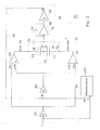
- FIG. 3a represents the electrical diagram of an accelerometer 50 according to the present invention, which differs from the conventional accelerometer of FIG. 2 only in that it comprises a compensation stage 45.
- the elements common to Figure 2 are designated by the same references and will not be described again.
- the compensation stage 45 is introduced into the feedback loop 26 bringing on the excitation stage 21 the measurement voltage delivered by the processing stage 30, now designated by the term vd, the output voltage vs being taken at the output of loop 26, after the compensation stage 45, and conventionally applied to the amplifier 25 and to the demodulator 40.
- Stage 45 comprises an operational amplifier 46, the output of which is brought back to the negative input by a resistor 47.
- the voltages vd and v are applied to the input of the amplifier 46 by means of resistors 48 and 49, respectively.
- stage 45 can be adjusted by calibration on a test bench, or by construction, after theoretical or experimental determination of the parasitic capacities.
- the gain G, the gain a of the amplifier 25, as well as the gain b of the amplifier 24 are parameters for adjusting the accelerometer.
- a particularly simple embodiment consists in taking a, b, and G equal to 1.
- the voltage avs must be perfectly in phase with the voltages bv and -bv. It is within the reach of those skilled in the art to ensure that the sum of the phase shifts introduced by the different elements of the accelerometer 50 lead to this result.
- FIG. 4 represents an accelerometer 60 which is an alternative embodiment of that of FIG. 3a, having the additional advantage of not being sensitive to possible phase problems.
- the various voltages vs, v, avs, bv, and vd are direct voltages.
- the various elements making up the excitation stage of the system of FIG. 3a are preserved, and are designated under the same references.
- the amplifiers 22, 23 of the excitation stage 21 deliver direct voltages avs - bv, avs + bv, respectively. These voltages are chopped by switches 27, 28 (for example MOS transistors) controlled by a clock signal H, before being applied in the form of slots to the capacitors Cs, Ci.
- switches 27, 28 for example MOS transistors
- the processing stage 30 receiving the current from the capacitors Cs, Ci comprises the current / voltage converter 31 already described, the amplifier 33 being replaced by a demodulator 34 having a static gain G, synchronized with the clock signal H.
- the voltage vd from demodulator 34 is applied to the compensation stage 45 according to the invention, already described in relation to FIG. 3b, operating here in continuous mode.
- the output voltage vs coming from the compensation stage 45 is directly usable as an output signal Us.
- the accelerometer 60 operates in the same way as the accelerometer 50 of FIG. 3a, the relations (5) and (6) described above being always valid.
- the compensation stage 45 can be represented by the block diagram shown in FIG.
- the stage 45 comprises a first amplifier 452 of gain A - 1, receiving at input vd, a second amplifier 453 of gain B , receiving at input v, and an adder amplifier 454 receiving at input the outputs of amplifiers 452, 453 and delivering the correction signal vc, vc being injected into the feedback loop 26 by means of an adder 451 receiving at input vc and vd.
- SECOND PROCEDURE addition of a current compensation stage in the measurement system.
- I avs (C1 + C2) - bv (C1 - C2) (For the sake of simplicity, we have deleted in relations (7) and (8) the classical term expressing the periodicity of the signals, for example ⁇ if the signals are sinusoidal. Thus, the term I has the dimension of a current divided by a term of periodicity, and represents an electric charge).
- I cvs (Cn1 + Cn2) - dv (Cn1 - Cn2).
- relation (7) By means of the adjustment coefficients c and d, and possibly a and b, we make sure that the relation (8) is verified.
- FIG. 5 represents the electrical diagram of an accelerometer 80 comprising a stage 70 of current compensation.
- the accelerometer 80 comprises the excitation stage 21 and the processing stage 30 already described, operating here by cutting out DC voltages.
- the amplifiers 22, 23 drive the capacitors Cs, Ci via the two switches 27, 28 synchronized with the clock signal H, and the processing stage 30 comprises the demodulator 34, which here has a static gain G very high.
- the reference voltage v of the excitation stage 21 applied to the amplifier 24 is a direct voltage, and the voltage vs delivered by the demodulator 34 acts as an output signal Us of the accelerometer 80.
- the compensation stage 70 is mounted in parallel with the excitation stage 21 and the detector 1. It receives as input the voltage vs, brought by the feedback loop 26 and the reference voltage v. Its output is connected to node 14, that is to say at the input of processing stage 30, and delivers a current I for correcting the disturbing effect of the parasitic capacitances.
- Stage 70 comprises, at the input, an amplifier 71 of gain c, receiving the voltage vs and an amplifier 72 of gain d, receiving the voltage v.
- the output of amplifier 71 is connected to the positive input of a differential amplifier 73 and to an input of an adder amplifier 74.
- the output of amplifier 72 is connected to the negative input of amplifier 73 and to the other input of amplifier 74.
- the output of amplifier 73 drives a first compensation capacitor Cn1 via a chopper switch 75, and the output of amplifier 74 drives a second capacitor of compensation Cn2 by means of a chopper switch 76.
- the switches 75,76 are synchronized with the clock signal H and operate in phase opposition with the switches 27,28 of the excitation stage 21.
- the ends capacitors Cn1, Cn2 are connected to a node 77 which constitutes the output of the compensation stage 70, the node 77 being connected to node 14.
- the amplifiers 73,74 of the compensation stage deliver continuous voltages cvs - dv and cvs + dv chopped by the switches 75,76 before being applied to the capacitors Cn1, Cn2, and similarly the amplifiers 22 , 23 of the excitation stage deliver DC voltages avs - bv and avs + bv chopped by the switches 27,28 before being applied to the capacitors Cs, Ci.
- the expression of the output voltage vs delivered by the accelerometer 80 is given by the relation (7) and thus depends on the sum of the currents at node 14. As we explained previously, we neutralize the effect of the capacities parasites in the accelerometer 80 by choosing the parameters a, b, c, d so that the equality expressed by the relation (8) is reached. Just like the voltage compensation stage described in relation to FIGS. 3a and 4, the current compensation stage of FIG. 5 can be adjusted by calibration on a test bench, or by construction, after theoretical determination or experimental parasitic capacities.
- a particularly advantageous embodiment of the compensation stage 70 consists in providing compensation capacitors Cn1, Cn2 of the same technology as the detector, and preferably having capacities close to C1 and C2 in order to present the same thermal drifts. Thus, the system is correctly compensated regardless of its operating temperature.
- the accelerometer 80 also works with periodic voltages v and vs.
- the cutting switches 27, 28, 75, 76 are removed and the demodulator 34 is replaced by a very high gain amplifier G. It is also necessary to phase-shift the current I by 180 ° and demodulate the output voltage vs to obtain Us.
- the output signal Us of the accelerometer is of an electrical nature.
- the accelerometer means for transforming the output signal into a signal of another nature, for example optical, or means for coding the output signal.
- the present invention can also be applied to detectors comprising several pairs of measurement capacitors arranged in parallel, this type of detector being electrically equivalent to a detector with two capacitors.
Landscapes
- Physics & Mathematics (AREA)
- General Physics & Mathematics (AREA)
- Pressure Sensors (AREA)
- Indication And Recording Devices For Special Purposes And Tariff Metering Devices (AREA)
- Transmission And Conversion Of Sensor Element Output (AREA)
Claims (9)
- Beschleunigungsmesser (50, 60, 80), welcher umfasst:- einen kapazitiven Detektor (1) aus Silizium, der ein System aus zwei variablen Kondensatoren (Cs,Ci) bildet, deren Kapazitätsungleichgewicht eine Funktion der Beschleunigung ist, wobei die genannten Kondensatoren durch parallel-liegende parasitäre Kapazitäten gestört sind,- ein elektronisches Meßsystem (21,30,26) zur Messung des kapazitiven Ungleichgewichts des Detektors, wobei das Meßsystem eine die Beschleunigung wiedergebende Ausgangsspannung (vs) erzeugt und umfaßt:dadurch gekennzeichnet-- eine Erreger- bzw. Treiberstufe (21) zur Beaufschlagung der genannten Kondensatoren (Cs,Ci) mit Erregungs- bzw. Antriebsspannungen (avs - bv, avs + bv), die durch gewichtete Kombination einer Bezugsspannung (v) und der genannten Ausgangsspannung (vs) gebildet sind,-- eine Strom/Spannungs-Wandlerstufe (30), welche von jeweils jedem der genannten Kondensatoren abgegebene Ströme aufnimmt und eine Meßspannung (vd,vs) erzeugt,-- eine Rückkopplungsschleife (26) zur Rückführung der genannten Meßspannung (vs,vd) n die Erregungs- bzw. Antriebsstufe (21), wobei die genannte Ausgangsspannung (vs) am Ausgang der Rückkopplungsschleife abgenommen wird,
daß der Beschleunigungsmesser eine Kompensationsstufe (45,70) zur Kompensation der Störwirkung der parasitären Kapazitäten (C1,C2) in solcher Ausbildung und Anordnung aufweist, daß in das Meßsystem (21,30,26) ein elektrisches Korrektursignal (vc,I) eingeführt wird, das aus der genannten Bezugsspannung (v) und der genannten Meßspannung (vs,vd) abgeleitet ist und so gewählt ist, daß die genannte Ausgangsspannung (vs) im wesentlichen proportional dem Verhältnis aus der Differenz (Cs - Ci) und der Summe (Cs + Ci) der Kapazitäten der genannten Kondensatoren ist. - Beschleunigungsmesser (50,60) nach Anspruch 1, bei welchem die genannte Kompensationsstufe (45) in die Rückkopplungsschleife (26) eine Korrekturspannung (vc, (A - 1) vd + Bv) einführt, welche der Meßspannung (vd) zugefügt wird und so gewählt ist, daß die Ausgangsspannung (vs) gleich der gewichteten Summe (Avd + Bv) der Meßspannung (vd) und der Bezugsspannung (v) ist, wobei die Gewichtungskoeffizienten (A,B) der gewichteten Summe Einstell- bzw. Regelparameter der Kompensationsstufe darstellen.
- Beschleunigungsmesser (50,60) nach Anspruch 1, bei welchem die genannte Kompensationsstufe (45) einen in der Rückkopplungsschleife (26) in Reihe angeordneten und als Addiervorrichtung geschalteten Operationsverstärker (46) aufweist, dessen Ausgang über einen ersten Widerstand (47) an seinen Eingang rückgeführt ist, wobei die Meßspannung (vd) und die Bezugsspannung (v) vermittels eines zweiten (48) bzw. eines dritten (49) Widerstands dem gleichen Eingang zugeführt werden und das Verhältnis aus dem ersten und dem zweiten Widerstand und das Verhältnis aus dem ersten und dem dritten Widerstand die genannten Einstell- bzw. Regelparameter (A,B) der Kompensationsstufe darstellen.
- Beschleunigungsmesser (50) nach einem der Ansprüche 1 bis 3, bei welchem die Bezugsspannung (v), die Meßspannung (vd) und die Ausgangsspannung periodische Spannungen sind
- Beschleunigungsmesser (60) nach einem der Ansprüche 1 bis 3, bei welchem die Bezugsspannung (v), die Meßspannung (vd) und die Ausgangsspannung (vs) Gleichspannungen sind, die Erregungs- bzw. Antriebsstufe (21) Schalter (27,28) zur Unterbrechung der an die genannten Kondensatoren (Cs,Ci) angelegten Erregungs- bzw. Antriebsspannungen aufweist und die Wandlerstufe (30) einen Strom/Spannungs-Wandler (31) mit einem nachfolgenden Demodulator (34) aufweist.
- Beschleunigungsmesser (80) nach Anspruch 1, bei welchem die Kompensationsstufe (70) am Eingang der Konverter-bzw. Wandlerstufe (30) einen Korrekturstrom (-I) einführt, der zu den von den Kondensatoren (Cs,Ci) kommenden aufgenommenen Strömen hinzugefügt wird und so gewählt ist, daß er den auf die Erregung bzw. Beaufschlagung der parasitären Kapazitäten (C1,C2) zurückzuführenden Strom aufhebt.
- Beschleunigungsmesser (80) nach Anspruch 6, bei welchem der genannte Korrekturstrom (-I) von zwei Kompensationskondensatoren (Cn1,Cn2) geliefert wird, die mit Spannungen erregt bzw. beaufschlagt werden, die gleich der Differenz und der Summe einer zu der genannten Bezugsspannung (v) proportionalen Spannung und einer zu der genannten Meßspannung (vs) proportionalen Spannung (cvs) sind, wobei die Erregungs- bzw. Beaufschlagungsspannungen der Kompensationskondensatoren Einstell- bzw. Regelparameter der Kompensationsstufe darstellen.
- Beschleunigungsmesser (80) nach Anspruch 7, bei welchem die genannte Bezugsspannung (v), Ausgangsspannung (vs) und Meßspannung (vs) Gleichspannungen sind und die Erregungs- bzw. Beaufschlagungsspannungen der Detektorkondensatoren (Cs,Ci) und der Kompensationskondensatoren Cn1,Cn2) durch in Gegenphase betriebene Schalter (27,28,75,76) unterbrochen werden, wobei die Konverter- bzw. Wandlerstufe (30) einen Strom/Spannungswandler (32) mit einem nachfolgenden Demodulator (34) mit sehr hoher statischer Verstärkung (G) aufweist.
- Beschleunigungsmesser nach einem der Ansprüche 7 und 8, bei welchem die genannten Kompensationskondensatoren (Cn1,Cn2) eine Sandwich-Anordnung aus einer Siliziumoxydschicht und zwei Siliziumplättchen aufweisen.
Applications Claiming Priority (2)
| Application Number | Priority Date | Filing Date | Title |
|---|---|---|---|
| FR9300752A FR2700614B1 (fr) | 1993-01-19 | 1993-01-19 | Accéléromètre capacitif à circuit de correction de l'effet perturbateur de capacités parasites. |
| FR9300752 | 1993-01-19 |
Publications (2)
| Publication Number | Publication Date |
|---|---|
| EP0613012A1 EP0613012A1 (de) | 1994-08-31 |
| EP0613012B1 true EP0613012B1 (de) | 1997-07-23 |
Family
ID=9443366
Family Applications (1)
| Application Number | Title | Priority Date | Filing Date |
|---|---|---|---|
| EP94410002A Expired - Lifetime EP0613012B1 (de) | 1993-01-19 | 1994-01-17 | Kapazitiver Beschleunigungsmesser mit Schaltung zur Korrektur des störender Einflusses parasitärer Kapazitäten |
Country Status (5)
| Country | Link |
|---|---|
| US (1) | US5600066A (de) |
| EP (1) | EP0613012B1 (de) |
| JP (1) | JPH06281669A (de) |
| DE (1) | DE69404337T2 (de) |
| FR (1) | FR2700614B1 (de) |
Families Citing this family (24)
| Publication number | Priority date | Publication date | Assignee | Title |
|---|---|---|---|---|
| US5576483A (en) * | 1993-10-01 | 1996-11-19 | Hysitron Incorporated | Capacitive transducer with electrostatic actuation |
| FR2724463B1 (fr) * | 1994-09-12 | 1996-12-13 | Sagem | Procede de mesure d'une acceleration par un capteur a armature mobile et capteur d'acceleration pour mettre en oeuvre le procede |
| JP2586406B2 (ja) * | 1994-10-27 | 1997-02-26 | 日本電気株式会社 | 静電容量型加速度センサ |
| JP3216455B2 (ja) * | 1994-12-22 | 2001-10-09 | 株式会社村田製作所 | 容量型静電サーボ加速度センサ |
| US5808198A (en) * | 1997-05-19 | 1998-09-15 | The Charles Stark Draper Laboratory, Inc. | RF balanced capacitive vibration sensor system |
| DE19730443A1 (de) * | 1997-07-16 | 1999-01-21 | Deutsch Zentr Luft & Raumfahrt | Mikromechanische Vorrichtung |
| US6035694A (en) * | 1999-03-12 | 2000-03-14 | I/O Of Austin, Inc. | Method and apparatus for calibration of stray capacitance mismatch in a closed loop electro-mechanical accelerometer |
| DE19929767C2 (de) * | 1999-06-29 | 2002-06-13 | Litef Gmbh | Beschleunigungsmeßeinrichtung |
| US6386032B1 (en) | 1999-08-26 | 2002-05-14 | Analog Devices Imi, Inc. | Micro-machined accelerometer with improved transfer characteristics |
| US6868726B2 (en) * | 2000-01-20 | 2005-03-22 | Analog Devices Imi, Inc. | Position sensing with improved linearity |
| US6879056B2 (en) * | 2000-12-29 | 2005-04-12 | Intel Corporation | Converting sensed signals |
| KR100444235B1 (ko) * | 2002-12-10 | 2004-08-16 | 삼성전기주식회사 | 자기 및 가속도 동시 검출 방법 및 장치 |
| JP4515821B2 (ja) * | 2004-05-25 | 2010-08-04 | ルネサスエレクトロニクス株式会社 | 駆動回路、動作状態検出回路及び表示装置 |
| WO2007126731A2 (en) * | 2006-03-29 | 2007-11-08 | Rosemount Inc. | Capacitance sensing circuit |
| JP2009097932A (ja) * | 2007-10-15 | 2009-05-07 | Freescale Semiconductor Inc | 容量型検出装置 |
| US8499630B2 (en) * | 2008-03-31 | 2013-08-06 | Intel Corporation | Piezoelectric sensor dynamic range improvement |
| DE102008023535B4 (de) * | 2008-05-14 | 2011-05-12 | Texas Instruments Deutschland Gmbh | Elektronische Vorrichtung und Verfahren zur Auswertung einer variablen Kapazität |
| DE102009026496B4 (de) * | 2009-05-27 | 2022-04-28 | Robert Bosch Gmbh | Kompensationskapazität für einen kapazitiven Sensor |
| US8322216B2 (en) * | 2009-09-22 | 2012-12-04 | Duli Yu | Micromachined accelerometer with monolithic electrodes and method of making the same |
| US9032777B2 (en) * | 2011-09-16 | 2015-05-19 | Robert Bosch Gmbh | Linearity enhancement of capacitive transducers by auto-calibration using on-chip neutralization capacitors and linear actuation |
| US8890045B2 (en) * | 2012-03-01 | 2014-11-18 | Avago Technologies General Ip (Singapore) Pte. Ltd. | Optical encoder with a current regulating circuit for a light emitter |
| US10309997B2 (en) * | 2013-03-15 | 2019-06-04 | Infineon Technologies Ag | Apparatus and a method for generating a sensor signal indicating information on a capacitance of a variable capacitor comprising a variable capacitance |
| US20140372074A1 (en) * | 2013-06-14 | 2014-12-18 | Memsic, Inc. | Tip-over sensor |
| US12510556B2 (en) * | 2023-04-11 | 2025-12-30 | Atlantic Inertial Systems, Inc. | Micro-electrical-mechanical-systems (MEMS) accelerometer systems |
Family Cites Families (11)
| Publication number | Priority date | Publication date | Assignee | Title |
|---|---|---|---|---|
| US3877313A (en) * | 1973-07-23 | 1975-04-15 | Singer Co | Electrostatic accelerometer |
| US4009607A (en) * | 1975-12-24 | 1977-03-01 | The Bendix Corporation | Force measuring system including combined electrostatic sensing and torquing means |
| FR2454103A1 (fr) * | 1979-04-11 | 1980-11-07 | Sagem | Perfectionnements aux accelerometres pendulaires asservis |
| US4353254A (en) * | 1980-12-18 | 1982-10-12 | The Singer Company | Control circuit for electro-static accelerometer |
| FR2617607B1 (fr) * | 1987-06-30 | 1989-12-01 | Applic Gles Electrici Meca | Accelerometre pendulaire a reequilibrage et procede de fabrication d'un tel accelerometre |
| DE3831593A1 (de) * | 1988-09-15 | 1990-03-22 | Siemens Ag | Schaltungsanordnung mit einer einer mechanischen verstimmung ausgesetzten differentialkondensator-anordnung |
| JPH0623782B2 (ja) * | 1988-11-15 | 1994-03-30 | 株式会社日立製作所 | 静電容量式加速度センサ及び半導体圧力センサ |
| US5277053A (en) * | 1990-04-25 | 1994-01-11 | Litton Systems, Inc. | Square law controller for an electrostatic force balanced accelerometer |
| US5142921A (en) * | 1990-10-29 | 1992-09-01 | Litton Systems, Inc. | Force balance instrument with electrostatic charge control |
| US5343766A (en) * | 1992-02-25 | 1994-09-06 | C & J Industries, Inc. | Switched capacitor transducer |
| FR2689627B1 (fr) * | 1992-04-07 | 1997-06-20 | Sextant Avionique | Perfectionnement aux micro-capteurs pendulaires asservis. |
-
1993
- 1993-01-19 FR FR9300752A patent/FR2700614B1/fr not_active Expired - Fee Related
-
1994
- 1994-01-17 EP EP94410002A patent/EP0613012B1/de not_active Expired - Lifetime
- 1994-01-17 DE DE69404337T patent/DE69404337T2/de not_active Expired - Fee Related
- 1994-01-19 JP JP6017753A patent/JPH06281669A/ja not_active Withdrawn
-
1995
- 1995-09-01 US US08/522,224 patent/US5600066A/en not_active Expired - Lifetime
Also Published As
| Publication number | Publication date |
|---|---|
| JPH06281669A (ja) | 1994-10-07 |
| DE69404337D1 (de) | 1997-09-04 |
| DE69404337T2 (de) | 1997-11-20 |
| FR2700614A1 (fr) | 1994-07-22 |
| US5600066A (en) | 1997-02-04 |
| FR2700614B1 (fr) | 1995-04-14 |
| EP0613012A1 (de) | 1994-08-31 |
Similar Documents
| Publication | Publication Date | Title |
|---|---|---|
| EP0613012A1 (de) | Kapazitiver Beschleunigungsmesser mit Schaltung zur Korrektur des störender Einflusses parasitärer Kapazitäten | |
| EP2012101B1 (de) | Vorrichtung zur Detektion von elektromagnetischer Strahlung, insbesondere von Infrarotstrahlung | |
| EP1831652B1 (de) | Kapazitiver füllstandssensor und verfahren zur füllstandsschätzung | |
| EP2288871B1 (de) | Trägheitsdrehungssensor mit driftkompensation | |
| FR2776771A1 (fr) | Procede d'etalonnage en longueur d'onde d'un dispositif de filtrage d'un rayonnement electromagnetique | |
| EP0565462A1 (de) | Verbesserte Pendelmikrosensoren mit Kraftrückkopplung | |
| EP0510061B1 (de) | Vorrichtung zur messung der änderung der kapazität eines kondensators, insbesondere eines sensors | |
| EP0538184A1 (de) | Kapazitiver Positionsdetektor | |
| EP2933224A1 (de) | Messkreis | |
| WO2020002079A1 (fr) | Dispositif capacitif de détection de la présence d'une personne à proximité ou au contact d'un composant d'un véhicule automobile | |
| EP1835263B1 (de) | Elektronischer Schnittstellenschaltkreis eines kapazitiven Sensors zur Messung eines physikalischen Parameters und Verfahren zur Ingangsetzung des elektronischen Schaltkreises | |
| EP1960307A1 (de) | Mikroelektromechanisches system mit einem verformbaren teil und einem belastungssensor | |
| FR3065291A1 (fr) | Dispositif de detection de presence d'un occupant a l'interieur de l'habitacle d'un vehicule | |
| EP0346211B1 (de) | Die Eigenschaften eines Flüssigkristalles nutzender Berührungsschalter | |
| FR2594231A1 (fr) | Procede de mesure d'impedances en particulier de capacites faibles | |
| EP3695235B1 (de) | Impedanzmessvorrichtung | |
| EP0463919A1 (de) | Resonanz- und Richtungsmagnetometer | |
| CA2831350C (fr) | Procede de correction de la mesure d'une tension aux bornes d'un capteur | |
| EP1211888B1 (de) | Infrarotstrahlungsdetektionseinrichtung | |
| FR2620234A1 (fr) | Circuit de compensation en temperature pour accelerometre | |
| FR2706038A1 (fr) | Dispositif de mesure d'une force. | |
| FR2584207A1 (fr) | Circuit de commande pour un organe de reglage piezoelectrique | |
| FR2720510A1 (fr) | Dispositif de mesure d'une force. | |
| FR2473183A1 (fr) | Montage de circuit servant a convertir une variation de resistance en une variation de frequence | |
| WO2009103900A2 (fr) | Procede de correction de gain d'un organe capacitif et dispositif de mise en oeuvre |
Legal Events
| Date | Code | Title | Description |
|---|---|---|---|
| PUAI | Public reference made under article 153(3) epc to a published international application that has entered the european phase |
Free format text: ORIGINAL CODE: 0009012 |
|
| AK | Designated contracting states |
Kind code of ref document: A1 Designated state(s): CH DE FR GB IT LI |
|
| 17P | Request for examination filed |
Effective date: 19950208 |
|
| GRAG | Despatch of communication of intention to grant |
Free format text: ORIGINAL CODE: EPIDOS AGRA |
|
| 17Q | First examination report despatched |
Effective date: 19961016 |
|
| GRAH | Despatch of communication of intention to grant a patent |
Free format text: ORIGINAL CODE: EPIDOS IGRA |
|
| GRAH | Despatch of communication of intention to grant a patent |
Free format text: ORIGINAL CODE: EPIDOS IGRA |
|
| GRAA | (expected) grant |
Free format text: ORIGINAL CODE: 0009210 |
|
| AK | Designated contracting states |
Kind code of ref document: B1 Designated state(s): CH DE FR GB IT LI |
|
| REG | Reference to a national code |
Ref country code: CH Ref legal event code: EP |
|
| REG | Reference to a national code |
Ref country code: CH Ref legal event code: NV Representative=s name: MOINAS KIEHL SAVOYE & CRONIN |
|
| REF | Corresponds to: |
Ref document number: 69404337 Country of ref document: DE Date of ref document: 19970904 |
|
| GBT | Gb: translation of ep patent filed (gb section 77(6)(a)/1977) |
Effective date: 19970905 |
|
| ITF | It: translation for a ep patent filed | ||
| PLBE | No opposition filed within time limit |
Free format text: ORIGINAL CODE: 0009261 |
|
| STAA | Information on the status of an ep patent application or granted ep patent |
Free format text: STATUS: NO OPPOSITION FILED WITHIN TIME LIMIT |
|
| 26N | No opposition filed | ||
| REG | Reference to a national code |
Ref country code: GB Ref legal event code: IF02 |
|
| PGFP | Annual fee paid to national office [announced via postgrant information from national office to epo] |
Ref country code: GB Payment date: 20050112 Year of fee payment: 12 |
|
| PG25 | Lapsed in a contracting state [announced via postgrant information from national office to epo] |
Ref country code: IT Free format text: LAPSE BECAUSE OF NON-PAYMENT OF DUE FEES;WARNING: LAPSES OF ITALIAN PATENTS WITH EFFECTIVE DATE BEFORE 2007 MAY HAVE OCCURRED AT ANY TIME BEFORE 2007. THE CORRECT EFFECTIVE DATE MAY BE DIFFERENT FROM THE ONE RECORDED. Effective date: 20050117 |
|
| PG25 | Lapsed in a contracting state [announced via postgrant information from national office to epo] |
Ref country code: GB Free format text: LAPSE BECAUSE OF NON-PAYMENT OF DUE FEES Effective date: 20060117 |
|
| GBPC | Gb: european patent ceased through non-payment of renewal fee |
Effective date: 20060117 |
|
| PGFP | Annual fee paid to national office [announced via postgrant information from national office to epo] |
Ref country code: DE Payment date: 20070111 Year of fee payment: 14 |
|
| PG25 | Lapsed in a contracting state [announced via postgrant information from national office to epo] |
Ref country code: DE Free format text: LAPSE BECAUSE OF NON-PAYMENT OF DUE FEES Effective date: 20080801 |
|
| PGFP | Annual fee paid to national office [announced via postgrant information from national office to epo] |
Ref country code: FR Payment date: 20110128 Year of fee payment: 18 Ref country code: CH Payment date: 20110112 Year of fee payment: 18 |
|
| REG | Reference to a national code |
Ref country code: CH Ref legal event code: PL |
|
| REG | Reference to a national code |
Ref country code: FR Ref legal event code: ST Effective date: 20120928 |
|
| PG25 | Lapsed in a contracting state [announced via postgrant information from national office to epo] |
Ref country code: CH Free format text: LAPSE BECAUSE OF NON-PAYMENT OF DUE FEES Effective date: 20120131 Ref country code: LI Free format text: LAPSE BECAUSE OF NON-PAYMENT OF DUE FEES Effective date: 20120131 |
|
| PG25 | Lapsed in a contracting state [announced via postgrant information from national office to epo] |
Ref country code: FR Free format text: LAPSE BECAUSE OF NON-PAYMENT OF DUE FEES Effective date: 20120131 |