EP0613128A1 - Support optique d'informations - Google Patents
Support optique d'informations Download PDFInfo
- Publication number
- EP0613128A1 EP0613128A1 EP94200365A EP94200365A EP0613128A1 EP 0613128 A1 EP0613128 A1 EP 0613128A1 EP 94200365 A EP94200365 A EP 94200365A EP 94200365 A EP94200365 A EP 94200365A EP 0613128 A1 EP0613128 A1 EP 0613128A1
- Authority
- EP
- European Patent Office
- Prior art keywords
- layer
- information carrier
- optical information
- reflection
- auxiliary layer
- Prior art date
- Legal status (The legal status is an assumption and is not a legal conclusion. Google has not performed a legal analysis and makes no representation as to the accuracy of the status listed.)
- Withdrawn
Links
Images
Classifications
-
- G—PHYSICS
- G11—INFORMATION STORAGE
- G11B—INFORMATION STORAGE BASED ON RELATIVE MOVEMENT BETWEEN RECORD CARRIER AND TRANSDUCER
- G11B7/00—Recording or reproducing by optical means, e.g. recording using a thermal beam of optical radiation by modifying optical properties or the physical structure, reproducing using an optical beam at lower power by sensing optical properties; Record carriers therefor
- G11B7/24—Record carriers characterised by shape, structure or physical properties, or by the selection of the material
- G11B7/241—Record carriers characterised by shape, structure or physical properties, or by the selection of the material characterised by the selection of the material
- G11B7/252—Record carriers characterised by shape, structure or physical properties, or by the selection of the material characterised by the selection of the material of layers other than recording layers
-
- G—PHYSICS
- G11—INFORMATION STORAGE
- G11B—INFORMATION STORAGE BASED ON RELATIVE MOVEMENT BETWEEN RECORD CARRIER AND TRANSDUCER
- G11B7/00—Recording or reproducing by optical means, e.g. recording using a thermal beam of optical radiation by modifying optical properties or the physical structure, reproducing using an optical beam at lower power by sensing optical properties; Record carriers therefor
- G11B7/24—Record carriers characterised by shape, structure or physical properties, or by the selection of the material
- G11B7/241—Record carriers characterised by shape, structure or physical properties, or by the selection of the material characterised by the selection of the material
- G11B7/242—Record carriers characterised by shape, structure or physical properties, or by the selection of the material characterised by the selection of the material of recording layers
- G11B7/243—Record carriers characterised by shape, structure or physical properties, or by the selection of the material characterised by the selection of the material of recording layers comprising inorganic materials only, e.g. ablative layers
- G11B2007/24302—Metals or metalloids
- G11B2007/24312—Metals or metalloids group 14 elements (e.g. Si, Ge, Sn)
-
- G—PHYSICS
- G11—INFORMATION STORAGE
- G11B—INFORMATION STORAGE BASED ON RELATIVE MOVEMENT BETWEEN RECORD CARRIER AND TRANSDUCER
- G11B7/00—Recording or reproducing by optical means, e.g. recording using a thermal beam of optical radiation by modifying optical properties or the physical structure, reproducing using an optical beam at lower power by sensing optical properties; Record carriers therefor
- G11B7/24—Record carriers characterised by shape, structure or physical properties, or by the selection of the material
- G11B7/241—Record carriers characterised by shape, structure or physical properties, or by the selection of the material characterised by the selection of the material
- G11B7/242—Record carriers characterised by shape, structure or physical properties, or by the selection of the material characterised by the selection of the material of recording layers
- G11B7/243—Record carriers characterised by shape, structure or physical properties, or by the selection of the material characterised by the selection of the material of recording layers comprising inorganic materials only, e.g. ablative layers
- G11B2007/24302—Metals or metalloids
- G11B2007/24314—Metals or metalloids group 15 elements (e.g. Sb, Bi)
-
- G—PHYSICS
- G11—INFORMATION STORAGE
- G11B—INFORMATION STORAGE BASED ON RELATIVE MOVEMENT BETWEEN RECORD CARRIER AND TRANSDUCER
- G11B7/00—Recording or reproducing by optical means, e.g. recording using a thermal beam of optical radiation by modifying optical properties or the physical structure, reproducing using an optical beam at lower power by sensing optical properties; Record carriers therefor
- G11B7/24—Record carriers characterised by shape, structure or physical properties, or by the selection of the material
- G11B7/241—Record carriers characterised by shape, structure or physical properties, or by the selection of the material characterised by the selection of the material
- G11B7/242—Record carriers characterised by shape, structure or physical properties, or by the selection of the material characterised by the selection of the material of recording layers
- G11B7/243—Record carriers characterised by shape, structure or physical properties, or by the selection of the material characterised by the selection of the material of recording layers comprising inorganic materials only, e.g. ablative layers
- G11B2007/24302—Metals or metalloids
- G11B2007/24316—Metals or metalloids group 16 elements (i.e. chalcogenides, Se, Te)
-
- G—PHYSICS
- G11—INFORMATION STORAGE
- G11B—INFORMATION STORAGE BASED ON RELATIVE MOVEMENT BETWEEN RECORD CARRIER AND TRANSDUCER
- G11B7/00—Recording or reproducing by optical means, e.g. recording using a thermal beam of optical radiation by modifying optical properties or the physical structure, reproducing using an optical beam at lower power by sensing optical properties; Record carriers therefor
- G11B7/24—Record carriers characterised by shape, structure or physical properties, or by the selection of the material
- G11B7/241—Record carriers characterised by shape, structure or physical properties, or by the selection of the material characterised by the selection of the material
- G11B7/252—Record carriers characterised by shape, structure or physical properties, or by the selection of the material characterised by the selection of the material of layers other than recording layers
- G11B7/257—Record carriers characterised by shape, structure or physical properties, or by the selection of the material characterised by the selection of the material of layers other than recording layers of layers having properties involved in recording or reproduction, e.g. optical interference layers or sensitising layers or dielectric layers, which are protecting the recording layers
- G11B2007/25705—Record carriers characterised by shape, structure or physical properties, or by the selection of the material characterised by the selection of the material of layers other than recording layers of layers having properties involved in recording or reproduction, e.g. optical interference layers or sensitising layers or dielectric layers, which are protecting the recording layers consisting essentially of inorganic materials
- G11B2007/25706—Record carriers characterised by shape, structure or physical properties, or by the selection of the material characterised by the selection of the material of layers other than recording layers of layers having properties involved in recording or reproduction, e.g. optical interference layers or sensitising layers or dielectric layers, which are protecting the recording layers consisting essentially of inorganic materials containing transition metal elements (Zn, Fe, Co, Ni, Pt)
-
- G—PHYSICS
- G11—INFORMATION STORAGE
- G11B—INFORMATION STORAGE BASED ON RELATIVE MOVEMENT BETWEEN RECORD CARRIER AND TRANSDUCER
- G11B7/00—Recording or reproducing by optical means, e.g. recording using a thermal beam of optical radiation by modifying optical properties or the physical structure, reproducing using an optical beam at lower power by sensing optical properties; Record carriers therefor
- G11B7/24—Record carriers characterised by shape, structure or physical properties, or by the selection of the material
- G11B7/241—Record carriers characterised by shape, structure or physical properties, or by the selection of the material characterised by the selection of the material
- G11B7/252—Record carriers characterised by shape, structure or physical properties, or by the selection of the material characterised by the selection of the material of layers other than recording layers
- G11B7/257—Record carriers characterised by shape, structure or physical properties, or by the selection of the material characterised by the selection of the material of layers other than recording layers of layers having properties involved in recording or reproduction, e.g. optical interference layers or sensitising layers or dielectric layers, which are protecting the recording layers
- G11B2007/25705—Record carriers characterised by shape, structure or physical properties, or by the selection of the material characterised by the selection of the material of layers other than recording layers of layers having properties involved in recording or reproduction, e.g. optical interference layers or sensitising layers or dielectric layers, which are protecting the recording layers consisting essentially of inorganic materials
- G11B2007/25715—Record carriers characterised by shape, structure or physical properties, or by the selection of the material characterised by the selection of the material of layers other than recording layers of layers having properties involved in recording or reproduction, e.g. optical interference layers or sensitising layers or dielectric layers, which are protecting the recording layers consisting essentially of inorganic materials containing oxygen
-
- G—PHYSICS
- G11—INFORMATION STORAGE
- G11B—INFORMATION STORAGE BASED ON RELATIVE MOVEMENT BETWEEN RECORD CARRIER AND TRANSDUCER
- G11B7/00—Recording or reproducing by optical means, e.g. recording using a thermal beam of optical radiation by modifying optical properties or the physical structure, reproducing using an optical beam at lower power by sensing optical properties; Record carriers therefor
- G11B7/24—Record carriers characterised by shape, structure or physical properties, or by the selection of the material
- G11B7/241—Record carriers characterised by shape, structure or physical properties, or by the selection of the material characterised by the selection of the material
- G11B7/252—Record carriers characterised by shape, structure or physical properties, or by the selection of the material characterised by the selection of the material of layers other than recording layers
- G11B7/258—Record carriers characterised by shape, structure or physical properties, or by the selection of the material characterised by the selection of the material of layers other than recording layers of reflective layers
- G11B7/2595—Record carriers characterised by shape, structure or physical properties, or by the selection of the material characterised by the selection of the material of layers other than recording layers of reflective layers based on gold
Definitions
- the invention relates to an optical information carrier for inscribing, reading and erasing information by means of a laser-light beam, said optical information carrier comprising a transparent substrate having a servotrack and a stack of layers, which stack comprises at least one recording layer of a phase-change material and at least one reflection layer of metal.
- Known optical information carriers such as the Compact Disc (CD), Compact Disc Read-Only-Memory (CD-ROM) and Laser Vision (LV) are provided with information by the manufacturer and can only be read by the user by means of commercially available playback quipment.
- Other information carriers can be recorded once (CD-R) by the user.
- CD-R Compact Disc
- a information carrier which is recordable and erasable by the user and which is readable in a standard CD player could be used for many applications.
- a special recording/erase device is used for recording and erasing. Audio or data information can be recorded in the information carrier by the user himself. After an erasing step, new information can be recorded in the information carrier.
- a prerequisite for reading a recordable and erasable information carrier in a standard CD player is that said information carrier is compatible with said CD player, i.e. it must comply with the industrial standard for CD systems, hereinafter referred to as CD-industrial standard.
- CD-industrial standard This means, among other things, that the reflection R H of unrecorded areas of the information carrier and the modulation must have a specific minimum value.
- the peak-to-peak value of the photocurrent is designated I11 and the top level of the HF signal associated with 196 kHz is designated I top .
- the modulation is defined as I11/I top and must be at least 0.6 according to the above-mentioned CD-industrial standard.
- the modulated photocurrent is caused by reflection differences and/or optical path-length differences between recorded and unrecorded areas of the information carrier. Information carriers whose modulation is based only on reflection differences must have a minimal optical contrast in order to attain the required modulation of 0.6.
- the modulation is lower than the optical contrast due to the size of the laser spot. This means that, in order to meet the modulation requirement of 0.6, the optical contrast C must be higher than 60%.
- the reflection requirement R H of unrecorded areas is based on a laser wavelength of 780 nm ⁇ 10 nm. For a perpendicularly incident, parallel laser-light beam of the above wavelength, the reflection of the substrate surface (approximately 4%) also being measured, R H must be at least 70%. In the case of a focused laser-light beam, as used in a CD player, a reflection value R H of minimally 65% is sufficient, i.e. such a information carrier can be played in a standard CD player and is compatible therewith.
- a known type of optical information carrier has a recording layer of a so-called phase-change material.
- phase-change material By locally heating said recording layer with a focused laser-light beam and subsequently cooling it, the state of crystallization of these materials is changed at the location of the laser spot and a readable bit is formed.
- amorphous material changes to crystalline material or conversely. Conversion of a crystalline phase to another crystalline phase is also possible.
- the recording layer is, for example, crystalline and has the property that incident laser light is absorbed.
- the information carrier is rotated and exposed to a focused laser-light beam which is modulated in accordance with the information to be inscribed.
- amorphous information bits are formed in the exposed areas of the recording layer which remains crystalline in the unexposed areas.
- the crystalline material has other optical properties than the amorphous material, so that the recorded information can be read in reflection as an optical contrast by means of a low-power, focused laser-light beam.
- the amorphous areas can be reconverted into crystalline areas, or conversely, by heating, so that the recorded information is erased. Subsequently, new information can again be recorded in the recording layer.
- a information carrier of the type mentioned in the opening paragraph is known from European Patent Application EP-A-352105.
- the known information carrier of the phase-change type consists of a substrate which is provided with a spiral-shaped servotrack which carries a stack of layers consisting of a recording layer of an InSb or TeGe alloy, a dielectric layer of, for example, ZnS and a reflection layer of, for example, Au.
- the reflections amount to 72% and 38% for the unrecorded and the recorded areas, respectively.
- the measured optical contrast and hence the modulation which, as described above, is lower than the optical contrast do not comply with said CD-industrial standard (modulation > 0.6).
- the stack has an MIPIM layer structure, where M is a metal layer, I a dielectric layer and P a phase-change recording layer.
- the described information carrier comprises, for example, a thin Au reflection layer, a Ta2O5 dielectric layer, a (write once) GeTe recording layer, a Ta2O5 dielectric layer and an optically tight Au layer. Due to interference effects, both the initial reflection and the contrast of the information carrier are increased. For said layer structure, the reflections of the unrecorded and recorded areas are 70% and 12%, respectively. Thus, the optical contrast C is 82% and hence complies with the CD-industrial standard.
- a problem of the recorded information carrier which complies with the CD standard is, however, that the absorption of the laser-light beam in an unrecorded area can maximally amount to 35% due to the fact that the reflection of the unrecorded areas must be at least 65%. Consequently, the write-sensitivity of the information carrier is so small that an unusually large laser power is required for the write process.
- CD-E erasable optical information carrier
- an optical information carrier as described in the opening paragraph, which is characterized in that the stack also comprises at least one auxiliary layer having the property that the light absorption has a reversible, temperature-dependent character, so that at temperatures below 70°C the light absorption of the auxiliary layer is zero or substantially zero and at temperatures above 70°C the light absorption of the stack increases to more than 35%.
- the invention is based on the insight that the CD requirements as regards reflection and modulation of the information carrier apply only for temperatures between -40°C and +70°C, i.e. in the operating range of the CD system. At temperatures above +70°C, a drastic decrease in reflection and hence a drastic increase in absorption are permitted.
- phase transition is the transition from the ordered state to the disordered state, such as melting, or the transition from crystalline to amorphous and the transition from the liquid-crystalline phase to the isotropic phase.
- the transition from crystalline to crystalline is also possible. Said transitions can also take place in the opposite direction.
- the layer which exhibits a phase transition is located in a position where most laser light is incident on it, preferably between the stack and the substrate.
- auxiliary layer When the temperature decreases to below 70°C, the original, optical state must be restored. Frequent switching between, for example, the solid and the liquid phase must be possible.
- the increase in write-sensitivity which can be obtained in this manner depends on the absorption increase to be attained. An absorption of 35% requires a writing power of the laser of, for example, 30 mW. An absorption increase up to 70% then requires 15 mW.
- the absorption of the auxiliary layer must be zero or substantially zero at room temperature ( i.e. at temperatures below 70°C).
- the auxiliary layer comprises Selenium (Se).
- the optical properties of selenium are governed by temperature. At room temperature and temperatures up to 70°C selenium is substantially non-absorbent at the laser wavelength used. Above the melting point of selenium (217°C) the auxiliary layer is sufficiently absorbent. If a selenium auxiliary layer is used, the reflection of the information carrier decreases drastically above the melting point of selenium.
- the temperature of the information carrier rises to, for example, 600°C and the selenium auxiliary layer melts. This causes a substantial increase in absorption, so that the write process can be carried out with a lower laser power.
- the selenium auxiliary layer solidifies and its absorption becomes substantially zero again.
- the reflection of the erased information carrier and hence of the unrecorded areas increases again to more than 65% and, hence, satisfies the requirement of the CD-industrial standard.
- the auxiliary layer comprises selenium to which 1-6 at. % of tellurium is added. Said addition causes the absorption coefficient k of the auxiliary layer to be further increased in the molten phase. In the solid phase, the absorption coefficient k of a selenium layer comprising 3 at. % of tellurium is small (0.038) and increases to 0.14 in the molten phase.
- a suitable choice of the thickness of the auxiliary layer enables an absorption increase of the auxiliary layer and the other layers of the stack to be attained, which ranges from 35% at room temperature to 55% in the hot state (approximately 250°C), as exists during recording or erasing. By virtue thereof, the laser power necessary for recording or erasing can be reduced by approximately 25%.
- AlGaAs AlGaAs
- a property of this and other semi-conducting materials is that the spectral absorption band shifts with temperature.
- the absorption band of AlGaAs shifts approximately 40 nm per 100°C.
- the absorption of AlGaAs at room temperature can be adjusted so as to be substantially equal to zero for the required laser wavelength by blending GaAs with the proper concentration of Al. In this manner, a change of the absorption coefficient k of from 0.0006 to 0.06 at a temperature increase of 200°C can be attained at the desired wavelength.
- This material has the advantage that its absorption at room temperature is lower than that of Se comprising a few per cent of Te. This has a favourable effect on the optical contrast and hence on the modulation.
- An increased absorption at temperatures above 70°C can be obtained by choosing a suitable AlGaAs layer thickness.
- a suitable AlGaAs layer thickness For a 190 nm thick auxiliary layer of AlGaAs, the combined absorption of the auxiliary layer and the recording layer can increase from 30% to 48% at a temperature increase of 200°C.
- the auxiliary layer is bounded by one or more dielectric layers.
- the dielectric layers may have a thickness such that they serve as interference layers to increase reflection.
- the recording layer comprises a phase-change material which exhibits, for example, a crystalline-amorphous phase transition.
- amorphous information bits are formed in an otherwise crystalline recording layer.
- the phase-change materials used are reversible, so that the recorded information can be erased after which the material can be recorded again.
- Known materials of this type are the alloys of In-Se, In-Se-Sb, In-Sb-Te, Te-Ge, Te-Se-Sb, Te-Ge-Sb and Te-Ge-Se-Sb. If a recording layer of such a material is used in a information carrier in accordance with the invention, an recordable and erasable information carrier which is CD compatible (CD-E) is obtained.
- the simplest embodiment of the information carrier in accordance with the invention has the following structure: SPHM, where S denotes the substrate, P denotes the recording layer, H denotes the auxiliary layer, whether or not bounded by one or more dielectric layers, and M denotes the metal reflection layer.
- a dielectric layer I is present between the recording layer and the metal reflection layer, so that the following structure is obtained: SHPIM.
- the thickness of the dielectric layer may be such that said layer serves as an interference layer to increase the optical contrast.
- the auxiliary layer H may also be located elsewhere in the stack.
- a second reflection layer M' and a second dielectric layer is located between the substrate and the recording layer, said second dielectric layer being adjacent to the recording layer.
- the information carrier has the following structure: SEM'IPIM.
- the auxiliary layer H whether or not bounded by dielectric layers, may also be located elsewhere in the stack.
- a variant is, for example, SM'HPIM, where H is bounded by two dielectric layers.
- the reflection layer M' which is situated on the substrate side may consist of a metal or metal alloy of the elements Au, Al, Cu and Ag. Said reflection layer M' is optically non-tight and has a transmission coefficient in excess of, for example, 0.2.
- the reflection layer M' may alternatively be a dielectric reflector consisting of a stack of dielectric layers having alternately a high and a low refractive index, for example Ta2O5 and SiO2, respectively.
- the auxiliary layer H may form part of the layer stack of the dielectric reflector M'.
- the reflection layer M on the outside of the information carrier is preferably an optically tight metal layer of, for example, a metal or metal alloy of the elements Au, Al, Cu or Ag, so that the reflection layer transmits as little laser light as possible and, hence, as much laser light as possible is used for reading and the reflection of the information carrier is as high as possible.
- a possible structure is, for example, SIM'IPIM, which layer stack also comprises the auxiliary layer H. Also in this structure, the auxiliary layer H may form part of the layer stack of the dielectric reflector M'.
- the customary materials such as SiO2, TiO2, Si3N4, ZnS, AlN or Ta2O5. Mixtures of said materials, such as mixtures of ZnS and SiO2, can alternatively be used.
- the substrate of the information carrier is at least transparent to the laser wavelength of 780 nm ⁇ 10 nm used and consists of, for example, polycarbonate, polymethyl methacrylate (PMMA) or glass.
- the substrate must also be transparent to the laser wavelength used to record and erase.
- the thickness of the substrate is 1.2 mm and the diameter is 120 mm.
- the surface of the substrate is provided with an optically scannable servotrack on the side of the recording layer.
- This servotrack is generally a spiral-shaped groove and is provided in the substrate by means of a mould during injection-moulding or pressing.
- this groove can also be provided in a separate synthetic resin layer of, for example, a UV light-cured layer of acrylates, which is provided on the substrate.
- Such a groove has a pitch of 1.6 ⁇ m and a width of for example 0.6 ⁇ m.
- the outermost layer of the stack may be shielded from the environment by means of a protective coating of, for example, UV light-cured poly(meth)acrylate.
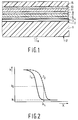
- Fig. 1 diagrammatically shows a part of a cross-section of an optical information carrier in accordance with the invention.
- Reference numeral 1 denotes a disc-shaped substrate of polycarbonate having a diameter of 120 mm and a thickness of 1.2 mm.
- One side of the substrate is provided with a spiral-shaped servotrack (not shown) in the form of a groove. This servotrack is formed in the polycarbonate in an injection-moulding process by using a suitable mould.
- the substrate On the side where the servotrack is formed, the substrate is provided with a 112 nm thick auxiliary layer 3 of an alloy of selenium and 3 at. % of tellurium.
- the top side ad the bottom side of the auxiliary layer 3 are provided with dielectric layers 2 and 4 of Ta2O5 which have a thickness of 5 nm.
- the dielectric layer 4 is provided with a stack of the following structure:
- the auxiliary layer is bounded by dielectric layers 2 and 4 of Ta2O5 having a thickness of 5 nm.
- the dielectric layer 4 is provided with a stack of the following structure:
Landscapes
- Optical Record Carriers And Manufacture Thereof (AREA)
- Thermal Transfer Or Thermal Recording In General (AREA)
Priority Applications (1)
| Application Number | Priority Date | Filing Date | Title |
|---|---|---|---|
| EP94200365A EP0613128A1 (fr) | 1993-02-18 | 1994-02-11 | Support optique d'informations |
Applications Claiming Priority (3)
| Application Number | Priority Date | Filing Date | Title |
|---|---|---|---|
| EP93200466 | 1993-02-18 | ||
| EP93200466 | 1993-02-18 | ||
| EP94200365A EP0613128A1 (fr) | 1993-02-18 | 1994-02-11 | Support optique d'informations |
Publications (1)
| Publication Number | Publication Date |
|---|---|
| EP0613128A1 true EP0613128A1 (fr) | 1994-08-31 |
Family
ID=26133663
Family Applications (1)
| Application Number | Title | Priority Date | Filing Date |
|---|---|---|---|
| EP94200365A Withdrawn EP0613128A1 (fr) | 1993-02-18 | 1994-02-11 | Support optique d'informations |
Country Status (1)
| Country | Link |
|---|---|
| EP (1) | EP0613128A1 (fr) |
Cited By (1)
| Publication number | Priority date | Publication date | Assignee | Title |
|---|---|---|---|---|
| WO1999054875A3 (fr) * | 1998-04-20 | 1999-12-23 | Koninkl Philips Electronics Nv | Support d'informations optique reinscriptible |
Citations (6)
| Publication number | Priority date | Publication date | Assignee | Title |
|---|---|---|---|---|
| JPS57159692A (en) * | 1981-03-27 | 1982-10-01 | Sony Corp | Information recording medium |
| JPS62226446A (ja) * | 1986-03-28 | 1987-10-05 | Toshiba Corp | 光記録媒体 |
| EP0352105A2 (fr) * | 1988-07-22 | 1990-01-24 | Fujitsu Limited | Milieu pour disque optique |
| JPH02113453A (ja) * | 1988-10-24 | 1990-04-25 | Hitachi Ltd | 光ディスク |
| US5164290A (en) * | 1989-06-30 | 1992-11-17 | Dainippon Ink And Chemicals Inc. | Optical recording medium |
| EP0549024A1 (fr) * | 1991-12-12 | 1993-06-30 | Koninklijke Philips Electronics N.V. | Porteur d'information optique |
-
1994
- 1994-02-11 EP EP94200365A patent/EP0613128A1/fr not_active Withdrawn
Patent Citations (6)
| Publication number | Priority date | Publication date | Assignee | Title |
|---|---|---|---|---|
| JPS57159692A (en) * | 1981-03-27 | 1982-10-01 | Sony Corp | Information recording medium |
| JPS62226446A (ja) * | 1986-03-28 | 1987-10-05 | Toshiba Corp | 光記録媒体 |
| EP0352105A2 (fr) * | 1988-07-22 | 1990-01-24 | Fujitsu Limited | Milieu pour disque optique |
| JPH02113453A (ja) * | 1988-10-24 | 1990-04-25 | Hitachi Ltd | 光ディスク |
| US5164290A (en) * | 1989-06-30 | 1992-11-17 | Dainippon Ink And Chemicals Inc. | Optical recording medium |
| EP0549024A1 (fr) * | 1991-12-12 | 1993-06-30 | Koninklijke Philips Electronics N.V. | Porteur d'information optique |
Non-Patent Citations (3)
| Title |
|---|
| PATENT ABSTRACTS OF JAPAN vol. 12, no. 93 (P - 680) 28 March 1986 (1986-03-28) * |
| PATENT ABSTRACTS OF JAPAN vol. 14, no. 333 (P - 1078) 18 July 1990 (1990-07-18) * |
| PATENT ABSTRACTS OF JAPAN vol. 6, no. 267 (M - 182) 25 December 1982 (1982-12-25) * |
Cited By (2)
| Publication number | Priority date | Publication date | Assignee | Title |
|---|---|---|---|---|
| WO1999054875A3 (fr) * | 1998-04-20 | 1999-12-23 | Koninkl Philips Electronics Nv | Support d'informations optique reinscriptible |
| RU2232436C2 (ru) * | 1998-04-20 | 2004-07-10 | Конинклейке Филипс Электроникс Н.В. | Перезаписываемая оптическая информационная среда |
Similar Documents
| Publication | Publication Date | Title |
|---|---|---|
| JP4037057B2 (ja) | 再書込み可能な光学情報媒体 | |
| KR100770768B1 (ko) | 광 기록매체와 이 광 기록매체를 이용한 기록방법 | |
| US6528138B2 (en) | Optical information medium | |
| US5442619A (en) | Erasable optical recording medium with a reversible light absorption layer | |
| KR20020080423A (ko) | 광 정보매체와 그것의 용도 | |
| US5876822A (en) | Reversible optical information medium | |
| WO1999014764A1 (fr) | Support d'enregistrement optique et systeme de memoire optique | |
| JPWO1999014764A1 (ja) | 光記録媒体および光メモリー装置 | |
| JPH08153339A (ja) | 光ディスク | |
| US6901044B2 (en) | Optical information medium and its use | |
| KR100753968B1 (ko) | 다시 쓰기 가능한 광학 정보 기록매체 | |
| US5935672A (en) | Reversible optical information medium | |
| JPH09286175A (ja) | 光記録媒体 | |
| JPH09286174A (ja) | 光記録媒体 | |
| KR100854953B1 (ko) | 재기록가능한 광학 데이터 저장매체와 이 매체의 용도 | |
| EP0360466A1 (fr) | Support d'enregistrement d'information optique et méthode d'enregistrement et de reproduction | |
| EP0549024B1 (fr) | Support d'information optique | |
| EP0613128A1 (fr) | Support optique d'informations | |
| US5432048A (en) | Rewritable photochromic optical disc | |
| US5419937A (en) | Optical record carrier | |
| JP3444042B2 (ja) | 光学的情報記録用媒体および光記録方法 | |
| KR20050040440A (ko) | 광기록매체 | |
| JPH07130006A (ja) | 光学的情報記録媒体 |
Legal Events
| Date | Code | Title | Description |
|---|---|---|---|
| PUAI | Public reference made under article 153(3) epc to a published international application that has entered the european phase |
Free format text: ORIGINAL CODE: 0009012 |
|
| AK | Designated contracting states |
Kind code of ref document: A1 Designated state(s): AT BE CH DE FR GB IT LI |
|
| 17P | Request for examination filed |
Effective date: 19950228 |
|
| 17Q | First examination report despatched |
Effective date: 19971022 |
|
| GRAG | Despatch of communication of intention to grant |
Free format text: ORIGINAL CODE: EPIDOS AGRA |
|
| RAP3 | Party data changed (applicant data changed or rights of an application transferred) |
Owner name: KONINKLIJKE PHILIPS ELECTRONICS N.V. |
|
| GRAG | Despatch of communication of intention to grant |
Free format text: ORIGINAL CODE: EPIDOS AGRA |
|
| GRAH | Despatch of communication of intention to grant a patent |
Free format text: ORIGINAL CODE: EPIDOS IGRA |
|
| STAA | Information on the status of an ep patent application or granted ep patent |
Free format text: STATUS: THE APPLICATION IS DEEMED TO BE WITHDRAWN |
|
| 18D | Application deemed to be withdrawn |
Effective date: 19981212 |