EP0614080A2 - Appareil pour reconnaître la forme d'une plaquette semi-conductrice - Google Patents
Appareil pour reconnaître la forme d'une plaquette semi-conductrice Download PDFInfo
- Publication number
- EP0614080A2 EP0614080A2 EP94301426A EP94301426A EP0614080A2 EP 0614080 A2 EP0614080 A2 EP 0614080A2 EP 94301426 A EP94301426 A EP 94301426A EP 94301426 A EP94301426 A EP 94301426A EP 0614080 A2 EP0614080 A2 EP 0614080A2
- Authority
- EP
- European Patent Office
- Prior art keywords
- semiconductor wafer
- shape
- image
- recognizing
- illuminating
- Prior art date
- Legal status (The legal status is an assumption and is not a legal conclusion. Google has not performed a legal analysis and makes no representation as to the accuracy of the status listed.)
- Withdrawn
Links
Images


Classifications
-
- H—ELECTRICITY
- H10—SEMICONDUCTOR DEVICES; ELECTRIC SOLID-STATE DEVICES NOT OTHERWISE PROVIDED FOR
- H10P—GENERIC PROCESSES OR APPARATUS FOR THE MANUFACTURE OR TREATMENT OF DEVICES COVERED BY CLASS H10
- H10P72/00—Handling or holding of wafers, substrates or devices during manufacture or treatment thereof
- H10P72/50—Handling or holding of wafers, substrates or devices during manufacture or treatment thereof for positioning, orientation or alignment
- H10P72/53—Handling or holding of wafers, substrates or devices during manufacture or treatment thereof for positioning, orientation or alignment using optical controlling means
Definitions
- the present invention relates to an apparatus for recognizing the shape of a semiconductor wafer, capable of automatically recognizing the shape of a semiconductor wafer when the semiconductor wafer is being processed on a dicing apparatus or the like to enable the dicing apparatus or the like to process and handle the semiconductor wafer accurately and efficiently according to the shape of the semiconductor wafer even if the semiconductor wafer is chipped or cracked.
- the semiconductor wafer After fabricating a plurality of semiconductor chips on the surface of a semiconductor wafer, the semiconductor wafer is subjected to inspection to inspect the semiconductor chips with an IC tester provided with a prober and to a dicing process on a dicing apparatus.
- the automatic process In automatically processing the semiconductor wafer, the automatic process is designed to align the semiconductor wafer automatically on an assumption that the semiconductor wafer is circular.
- the following explanation will be made in connection with a dicing apparatus by way of example.
- the dicing apparatus which cuts narrow grooves in the surface of the semiconductor wafer with a cutting blade rotating at a high speed, is widely used for cutting the semiconductor wafer into semiconductor chips.
- the pattern of the semiconductor chips fabricated on the surface of the semiconductor wafer cannot be correctly positioned relative to the working position of the cutting blade by simply mounting the semiconductor wafer on the stage and hence the grooves cannot be accurately cut along desired lines on the semiconductor wafer without adjusting the position of the semiconductor wafer relative to the cutting blade.
- the position of the semiconductor wafer relative to the working position of the cutting blade is adjusted by moving the stage supporting the semiconductor wafer into the field of view of an image pickup device and bringing a specified position on the semiconductor wafer into alignment with a specified position in the field of view of a projector.
- the projector is located beforehand at a predetermined position relative to the working position of the cutting blade.
- the stage After thus determining the positional relation between the specified position on the surface of the semiconductor wafer and the working position of the cutting blade, the stage is moved by a precision stage moving mechanism to cut grooves accurately along the desired lines on the semiconductor wafer.
- the operation to adjust the position of the semiconductor wafer relative to the working position of the cutting blade is called an alignment operation.
- an image represented by the video signals provided by the TV camera is displayed on the screen of a monitor and the operator adjusts the position of the semiconductor wafer while observing the image displayed on the screen of the monitor.
- the automation of the dicing apparatus has been desired for the enhancement of productivity and the automation of the alignment operation has been realized.
- the automation of the alignment operation can be achieved by image processing the video signals provided by the TV camera.
- the identification of the lines and the rows of the semiconductor chips requires a comparatively short time if the specific points are positioned near the center of the field of view of the TV camera. If the specific points are located away from the center of the field of view of the TV camera, the automatic alignment operation requires a comparatively long time because the operation for pattern matching must be repeated many times.
- the semiconductor wafer has a circular or substantially circular shape. Therefore, the specific points are moved for the automatic alignment operation to move the specific points into the field of view of the TV camera on an assumption that the semiconductor wafer is circular, the semiconductor wafer is supported on the frame with its center substantially on the center of the frame and the direction of extension of the lines of the semiconductor chips is within a certain range relative to notches formed in the frame.
- the pattern matching operation is performed when the semiconductor wafer is thus positioned.
- the applicant of the present patent application disclosed a dicing apparatus which starts its operation after recognizing the shape of the semiconductor wafer in Japanese Unexamined Patent Publication (Kokai) No. 4-109652.
- a dicing apparatus capable of recognizing the shape of the semiconductor wafer by image processing is disclosed in Japanese Unexamined Patent Publication (Kokai) No. 4-233250.
- an image pickup device is disposed so that the specularly reflected light will not fall thereon.
- the surface of the semiconductor wafer is a highly accurate flat plane, most part of the illuminating light falling on the surface of the semiconductor wafer 100 is specularly reflected and little reflected light falls on the image pickup device and hence a region in the image corresponding to the semiconductor wafer is very dark.
- the flatness of the surface of the frame is not as high as that of the surface of the semiconductor wafer 100, a region in the image corresponding to the frame is somewhat dark because the surface of the frame has a comparatively high flatness.
- the surface of the adhesive sheet reflects the illuminating light irregularly, a region in the image corresponding to the surface of the adhesive sheet is bright. Accordingly, when processing the image to recognize the shape of the semiconductor wafer, the image is converted into a digital image by converting the brightness values of the image into digital values with reference to an appropriate threshold.
- the region in the image corresponding to the surface of the semiconductor wafer is brighter than the region of the same corresponding to the surface of the adhesive sheet when the surface of the semiconductor wafer is in a particular condition.
- the image data is inverted so that the images of bright surfaces are dark and the images of dark surfaces are bright, and then, the inverted image data is processed in the foregoing manner to recognize the shape of the semiconductor wafer.
- the automatic alignment operation is possible because the positions of the lines and the rows of the semiconductor chips can be specified, and useless machining time can be dispensed with when dicing the semiconductor wafer because only part of the semiconductor wafer needs to be cut for dicing.
- circuit patterns formed on the surface of the semiconductor wafer interfere with the perfect specular reflection of the incident illuminating light and causes part of the reflected light to fall on the image pickup device, which is inferred to be due to the diffraction of the light. If such a phenomenon occurs, the TV camera provides video signals representing a partly bright image of the semiconductor wafer. If the such image is digitized using the same threshold as that used for digitizing the image, the semiconductor wafer is recognized as a cracked semiconductor wafer and an accurate recognition of the shape of the semiconductor wafer is impossible.
- a warp in the wafer and irregularly finished surface of the wafer are other effects that make accurate shape recognition impossible.
- the present invention has been made in view of the foregoing problems and it is therefore an object of the present invention to provide a shape recognizing apparatus, for recognizing the shape of a semiconductor wafer, capable of stably and accurately recognizing the shape of a semiconductor wafer without being affected by the circuit pattern formed on the semiconductor wafer, a warp in the semiconductor wafer or the finish on the surface of the semiconductor wafer.
- the shape recognizing apparatus in accordance with the present invention comprises: an illuminating means for illuminating a semiconductor wafer; an image pickup means disposed so that the light specularly reflected by the semiconductor wafer will not directly fall thereon, and capable of picking up the image of the semiconductor wafer and of providing video signals representing the image; and a means for recognizing the shape of the semiconductor wafer by processing the video signals; wherein a first polarizing means is placed on an optical path along which the illuminating light emitted by the illuminating means travels, and a second polarizing means is placed on an optical path along which the light from the semiconductor wafer travels toward and falls on the image pickup means.
- the polarizing direction of the reflected light has a specific angle depending on the surface condition of the circuit pattern of the semiconductor wafer. Accordingly, most part of the light reflected by the circuit pattern formed on the semiconductor wafer toward the image pickup device is intercepted by the second polarizing means when the illuminating light is polarized by the first polarizing means, and the polarizing direction of the second polarizing means is inclined at a given angle to the polarizing direction of the first polarizing means.
- the shape recognizing apparatus in accordance to the present invention forms an image to achieve accurate shape recognition even if part of the illuminating light is reflected toward the image pickup device by the circuit pattern formed on the semiconductor wafer.
- Fig. 1 is a perspective view showing the fundamental constitution of a dicing apparatus.
- reference 100 indicates a semiconductor wafer to be diced; 11 indicates a cutting blade formed by bonding abrasive grains of diamond or the like with nickel or the like; 12 indicates a spindle motor holding the cutting blade 11 to rotate the cutting blade 11 at a high speed; 13 indicates a stage for fixedly supporting the semiconductor wafer 100 thereon by suction; 14 indicates a precision stage moving mechanism for moving the stage in the directions of the arrows, and 16, 17 and 18 indicate components including in an image pickup device for measuring the position of the semiconductor wafer 100 supported on the stage 13. The stage 13 supporting the semiconductor wafer 100 is moved relative to the rotating cutting blade 11 for dicing.
- the semiconductor wafer 100 may directly be held on the stage 13, it is usual to attach the semiconductor wafer 100 to an adhesive sheet and to hold the adhesive sheet fixedly on the stage 13 to prevent the semiconductor wafer 100 from breaking into pieces during dicing.
- an adhesive sheet 102 is attached to a frame 101 having a central opening formed by punching, the semiconductor wafer 100 is attached to the adhesive surface of the adhesive sheet 102 exposed in the central opening of the frame 101, and the frame 101 thus holding the semiconductor wafer 100 is fixedly mounted on the stage 13.
- the frame 101 thus holding the semiconductor wafer 100 is transported between processing stations.
- the image pickup device comprises an objective 16 which forms an enlarged image of the surface of the semiconductor wafer 100, a lens barrel 17 and a TV camera 18.
- the image pickup device provides video signals representing an enlarged image of the surface of the semiconductor wafer 100.
- the pattern of the semiconductor chips fabricated on the surface of the semiconductor wafer 100 cannot be correctly positioned relative to the working position of the cutting blade 11 by simply mounting the semiconductor wafer 100 on the stage 13 and hence the alignment operation is performed.
- the position of the semiconductor wafer 100 relative to the working position of the cutting blade 11 is adjusted by moving the stage 13 supporting the semiconductor wafer 100 into the field of view of the image pickup device and bringing a specified position on the semiconductor wafer 100 into alignment with a specified position in the field of view of a projector.
- the projector is located beforehand at a predetermined position relative to the working position of the cutting blade 11. After thus determining the positional relationship between the specified position on the surface of the semiconductor wafer 100 and the working position of the cutting blade 11, the stage 13 is moved by the precision stage moving mechanism 14 to accurately cut grooves on the semiconductor wafer 100.
- Automation of the alignment operation can be achieved by image processing the video signals provided by the TV camera 18.
- Fig. 2 is a plan view of a semiconductor wafer 100 held on an adhesive sheet 102 attached to a frame 101 for dicing on a dicing apparatus.
- a plurality of semiconductor chips 110 are fabricated on the semiconductor wafer 100 in a predetermined arrangement, and grooves are to be cut between the rows and lines of the semiconductor chips 110.
- points A to E are brought into the field of view of the TV camera 18, and the boundaries between the lines and the rows of the semiconductor chips 110 are detected.
- the stage 13 is turned so that the lines and rows of the semiconductor chips 110 are aligned with the axes of the moving mechanism, and the coordinates of the moving mechanism, in a state where the specified position on the semiconductor wafer 100 coincides with a specified position on the image formed by the TV camera 18, are stored in a memory.
- the identification of the lines and the rows of the semiconductor chips 110 using the points A to E can be achieved by a known pattern matching method or the like.
- the identification of the lines and the rows of the semiconductor chips 110 requires a comparatively short time if the points A to E are positioned near the center of the field of view of the TV camera 18. If the points A to E are located far from the center of the field of view of the TV camera 18, the automatic alignment operation requires a comparatively long time because the operation for pattern matching must be repeated many times.
- the semiconductor wafer has a circular or substantially circular shape. Therefore, the points A to E shown in Fig. 2 are moved, during the automatic alignment operation, into the field of view of the TV camera 18 on an assumption that the semiconductor wafer 100 is circular, the semiconductor wafer 100 is supported on the frame 101 with its center substantially on the center of the frame 101 and the direction of extension of the lines of the semiconductor chips 110 is within a certain range relative to notches formed in the frame 101. The pattern matching operation is performed when the semiconductor wafer 100 is thus positioned.
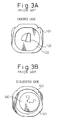
- Figs. 3A and 3B show a semiconductor wafer having an abnormal shape and a semiconductor wafer not correctly supported on the frame, respectively.
- the yield rate of the process will be reduced if cracked semiconductor wafers and chipped semiconductor wafers are thrown away. Therefore, defective semiconductor wafers must be diced, to provide normal semiconductor chips, like a semiconductor wafer 100 shown in Fig. 3A.
- Fig. 4 is a diagram showing a fundamental arrangement for detecting the shape of a semiconductor wafer using a TV camera.
- reference 1 indicates an illuminating device having a lamp 2 for illuminating a semiconductor wafer 100
- 3 indicates an image pickup system consisting of a lens unit 4 and a TV camera 5.
- Illuminating light emitted by the illuminating device 1 falls obliquely on the surface of the semiconductor wafer 100, and the image pickup device 3 is directed perpendicularly to the surface of the semiconductor wafer 100 to pick up the image of the semiconductor wafer 100.
- the image pickup device 3 is disposed so that the specularly reflected light will not fall thereon.
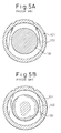
- the TV camera provides video signals representing an image as shown in Fig. 5A. Since the surface of the semiconductor wafer 100 is a highly accurate flat plane, most part of the illuminating light falling on the surface of the semiconductor wafer 100 is specularly reflected and little reflected light falls on the image pickup device 3 and hence a region in the image corresponding to the semiconductor wafer 100 is very dark. Although the flatness of the surface of the frame 101 is not as high as that of the surface of the semiconductor wafer 100, a region in the image corresponding to the frame 101 is somewhat dark because the surface of the frame 101 has a comparatively high flatness.
- the image is converted into a digital image by converting the brightness values of the image into digital values with reference to an appropriate threshold.
- the region in the image corresponding to the surface of the semiconductor wafer is brighter than the region corresponding to the surface of the adhesive sheet when the surface of the semiconductor wafer is in a particular condition.
- the image data is inverted so that the images of bright surfaces are dark and the images of dark surfaces are bright, and then, the inverted image data is processed in the foregoing manner to recognize the shape of the semiconductor wafer.
- the automatic alignment operation is possible because the positions for recognizing the lines and the rows of the semiconductor chips can be specified, and the useless machining time can be dispensed with when dicing the semiconductor wafer 100 because only necessary parts of the semiconductor wafer 100 need to be cut for dicing.
- the TV camera 5 provides video signals representing a partly bright image of the semiconductor wafer as shown in Fig. 5B. If the image as shown in Fig. 5B is subjected to digitization using the same threshold as that used for digitizing the image as shown in Fig. 7A, the semiconductor wafer 100 is recognized as a cracked semiconductor wafer and an accurate recognition of the shape of the semiconductor wafer 100 is impossible.
- Fig. 6 is a perspective view of a dicing apparatus incorporating a shape recognizing apparatus in a preferred embodiment according to the present invention.
- a cutting blade In Fig. 6, indicated at 11 is a cutting blade, and at 12 is a spindle motor for rotating the cutting blade 11 at a high rotating speed, capable of being moved in the directions of the arrows.
- a stage 13 for holding a semiconductor wafer 100 to be subjected to dicing is moved in the directions of the arrows by a stage moving mechanism 14. Moving mechanisms for moving the spindle motor 12 and the stage 13 are controlled by a controller 15.
- the semiconductor wafer 100 is attached to an adhesive sheet 102 attached to the frame 101 shown in Fig. 2, and the frame 101 holding the semiconductor wafer 100 is mounted on the stage 13.
- An image pickup device for forming an image of the semiconductor wafer 100 for the automatic alignment operation comprises a microscopic lens unit 16, a lens barrel 17 and a TV camera 18.
- the microscopic lens unit 16 forms enlarged images of the semiconductor wafer 100, the frame 101 and the adhesive sheet 102 on the TV camera 18, and then the TV camera 18 provides video signals representing the enlarged images.
- An automatic alignment unit 19 processes the video signals to identify a circuit pattern formed on the semiconductor wafer 100 and calculates the inclination of the circuit pattern relative to the screen and the position of the circuit pattern.
- the controller 15 turns the stage 13 to bring the lines of semiconductor chips into alignment with the axis of the stage moving mechanism 14 and moves the stage 13 to bring a specified position on the circuit pattern into coincidence with the center of the screen on the basis of calculated values provided by the automatic alignment unit 19. In this state, the controller 15 stores the coordinates-of the stage moving mechanism 14 as origin and controls the operation of the stage moving mechanism 14.
- the shape recognizing apparatus comprises an illuminating device 1 for illuminating the semiconductor wafer 100 when picking up an image of the semiconductor wafer 100 for shape recognition, an image pickup device 3, a shape recognizing unit 6 carries out image processing on the basis of video signals provided by the image pickup device 3 to recognize the shape of the semiconductor wafer 100, a first polarizing filter 7, and a second polarizing filter 8.
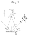
- Fig. 7 is a diagram showing optical paths along which light travels when picking up an image of the semiconductor wafer 100 using the shape recognizing apparatus.
- reference 2 indicates the lamp, i.e., the light source, of the illuminating device
- 4 indicates the objective of the image pickup device 3
- 5 indicates a TV camera.
- the optical paths shown in Fig. 7 will be described hereinafter.
- the polarizing direction of the first polarizing filter 7 is parallel to the paper.
- the illuminating light is reflected by the circuit pattern formed on the semiconductor wafer 100 and the reflected light P travels toward the-image pickup device 3.
- the polarizing direction of the reflected light has a specific angle which is dependent on the surface condition of the semiconductor wafer 100. Accordingly, most of the reflected light P is intercepted by the second polarizing filter having a polarizing direction perpendicular to the specified angle. Reflected light R reflected by the adhesive sheet 102 is irregularly reflected light and has random polarizing directions.
- the image of the adhesive sheet 102 is brighter than that of the semiconductor wafer 100. Since most of the light reflected toward the image pickup device 3 by the semiconductor wafer 100 is intercepted, no bright region will be formed in the image of the semiconductor wafer 100 even if reflectance varies from region to region on the surface of the semiconductor wafer 100. Consequently, the respective images of the semiconductor wafer 100 and the adhesive sheet 102 contrast sharply and hence accurate shape recognition can be achieved.
- the respective polarizing directions of the first polarizing filter 7 and the second polarizing filter 8 are substantially perpendicular to each other.
- the polarizing direction of the second filter 8 may be changed relative to the polarizing direction of the first filter 7 to adjust the brightnesses of the images so that accurate shape recognition can be achieved on the basis of the images.
- the shape recognizing apparatus for a semiconductor wafer in accordance with the present invention uses polarized illuminating light for illuminating the semiconductor wafer, and uses a polarizing filter for intercepting the reflected light reflected directly toward the image pickup device and, therefore, part of the reflected light directly reflected by the circuit pattern varying in reflectance from region to region is intercepted and, consequently, stable, accurate shape recognition can be achieved.
Landscapes
- Dicing (AREA)
- Container, Conveyance, Adherence, Positioning, Of Wafer (AREA)
- Length Measuring Devices By Optical Means (AREA)
- Testing Or Measuring Of Semiconductors Or The Like (AREA)
Applications Claiming Priority (2)
| Application Number | Priority Date | Filing Date | Title |
|---|---|---|---|
| JP45463/93 | 1993-03-05 | ||
| JP4546393A JPH06258056A (ja) | 1993-03-05 | 1993-03-05 | 半導体ウエハの形状認識装置 |
Publications (2)
| Publication Number | Publication Date |
|---|---|
| EP0614080A2 true EP0614080A2 (fr) | 1994-09-07 |
| EP0614080A3 EP0614080A3 (fr) | 1995-01-25 |
Family
ID=12720069
Family Applications (1)
| Application Number | Title | Priority Date | Filing Date |
|---|---|---|---|
| EP94301426A Withdrawn EP0614080A3 (fr) | 1993-03-05 | 1994-02-28 | Appareil pour reconnaître la forme d'une plaquette semi-conductrice. |
Country Status (2)
| Country | Link |
|---|---|
| EP (1) | EP0614080A3 (fr) |
| JP (1) | JPH06258056A (fr) |
Cited By (3)
| Publication number | Priority date | Publication date | Assignee | Title |
|---|---|---|---|---|
| DE102008007603B4 (de) * | 2007-02-02 | 2014-02-13 | Suss Microtec Test Systems Gmbh | Verfahren und Vorrichtung zur besseren Ausnutzung von Halbleitermaterial |
| CN109514744A (zh) * | 2017-09-19 | 2019-03-26 | 株式会社迪思科 | 晶片的加工方法 |
| US20210352835A1 (en) * | 2020-05-05 | 2021-11-11 | Integrated Dynamics Engineering Gmbh | Method for processing substrates, in particular wafers, masks or flat panel displays, with a semi-conductor industry machine |
Families Citing this family (5)
| Publication number | Priority date | Publication date | Assignee | Title |
|---|---|---|---|---|
| JP4728061B2 (ja) * | 2004-10-14 | 2011-07-20 | 株式会社ディスコ | 被加工物形状認識装置 |
| JP2014035733A (ja) * | 2012-08-10 | 2014-02-24 | Gunze Ltd | 撮像処理装置、撮像処理方法、ワーク加工システムおよびワーク加工方法 |
| JP7016730B2 (ja) * | 2018-03-09 | 2022-02-07 | リンテック株式会社 | 方位認識装置および方位認識方法、並びに、位置決め装置および位置決め方法 |
| JP7604298B2 (ja) * | 2021-03-24 | 2024-12-23 | 株式会社ディスコ | レーザー加工装置 |
| JP7848009B2 (ja) * | 2022-03-02 | 2026-04-20 | 株式会社ディスコ | 検査装置 |
Family Cites Families (7)
| Publication number | Priority date | Publication date | Assignee | Title |
|---|---|---|---|---|
| JPS5833108A (ja) * | 1981-08-21 | 1983-02-26 | Nec Home Electronics Ltd | ワ−ク外観検査方法 |
| JPS61108149A (ja) * | 1984-10-31 | 1986-05-26 | Kazumichi Kimura | 半導体ペレツトの位置検出装置 |
| JPH01114034A (ja) * | 1987-10-28 | 1989-05-02 | Hitachi Ltd | 半導体露光装置 |
| US5028138A (en) * | 1989-05-23 | 1991-07-02 | Wolff Lawrence B | Method of and apparatus for obtaining object data by machine vision form polarization information |
| JP3023566B2 (ja) * | 1990-08-30 | 2000-03-21 | 株式会社東京精密 | ダイシング装置 |
| JPH04233250A (ja) * | 1990-12-28 | 1992-08-21 | Matsushita Electron Corp | 半導体ダイシング装置 |
| DE4127707A1 (de) * | 1991-08-20 | 1993-02-25 | Siemens Ag | Verfahren zum ermitteln der orientierung des kristallgitters eines silizium-teils |
-
1993
- 1993-03-05 JP JP4546393A patent/JPH06258056A/ja active Pending
-
1994
- 1994-02-28 EP EP94301426A patent/EP0614080A3/fr not_active Withdrawn
Cited By (4)
| Publication number | Priority date | Publication date | Assignee | Title |
|---|---|---|---|---|
| DE102008007603B4 (de) * | 2007-02-02 | 2014-02-13 | Suss Microtec Test Systems Gmbh | Verfahren und Vorrichtung zur besseren Ausnutzung von Halbleitermaterial |
| CN109514744A (zh) * | 2017-09-19 | 2019-03-26 | 株式会社迪思科 | 晶片的加工方法 |
| CN109514744B (zh) * | 2017-09-19 | 2022-03-04 | 株式会社迪思科 | 晶片的加工方法 |
| US20210352835A1 (en) * | 2020-05-05 | 2021-11-11 | Integrated Dynamics Engineering Gmbh | Method for processing substrates, in particular wafers, masks or flat panel displays, with a semi-conductor industry machine |
Also Published As
| Publication number | Publication date |
|---|---|
| EP0614080A3 (fr) | 1995-01-25 |
| JPH06258056A (ja) | 1994-09-16 |
Similar Documents
| Publication | Publication Date | Title |
|---|---|---|
| US6014965A (en) | Apparatus for recognizing the shape of a semiconductor wafer | |
| US5504345A (en) | Dual beam sensor and edge detection system and method | |
| EP0493487B1 (fr) | Appareil d'inspection video a double image | |
| US6222624B1 (en) | Defect inspecting apparatus and method | |
| US5105147A (en) | Wafer inspection system | |
| US11177149B2 (en) | Wafer jig with identification mark | |
| US6038029A (en) | Method and apparatus for alignment of a wafer | |
| KR102824795B1 (ko) | 절삭 장치 및 절삭 장치를 사용한 웨이퍼의 가공 방법 | |
| JP2003501828A (ja) | ウエハ方向センサー | |
| JP2008267904A (ja) | 外観検査装置および表面状態の検査方法 | |
| US7180585B2 (en) | Apparatus for wafer inspection | |
| US12449378B2 (en) | Edge portion measuring apparatus and method for measuring edge portion | |
| US5962862A (en) | Method and apparatus for verifying the presence or absence of a component | |
| EP0614080A2 (fr) | Appareil pour reconnaître la forme d'une plaquette semi-conductrice | |
| JP2022114447A (ja) | ダイボンディング装置および半導体装置の製造方法 | |
| JP7826156B2 (ja) | 実装装置および半導体装置の製造方法 | |
| US6963394B2 (en) | Inspecting device for semiconductor wafer | |
| US7539338B2 (en) | Bump inspection apparatus and method for IC component, bump forming method for IC component, and mounting method for IC component | |
| JPH06326187A (ja) | ダイシング加工管理方法および加工品質管理システム | |
| US6128034A (en) | High speed lead inspection system | |
| KR20090066964A (ko) | 웨이퍼 결함 검출 장치 및 이의 방법 | |
| CN100529743C (zh) | 用光学方法控制较佳的具有圆形边缘物件的质量的方法和装置 | |
| JPH06260553A (ja) | ダイシング溝の位置測定方法 | |
| JPH02137339A (ja) | ペレットボンディング方法およびその装置 | |
| KR20030050746A (ko) | 반도체 웨이퍼 후면 연마 상태 검사장비 |
Legal Events
| Date | Code | Title | Description |
|---|---|---|---|
| PUAI | Public reference made under article 153(3) epc to a published international application that has entered the european phase |
Free format text: ORIGINAL CODE: 0009012 |
|
| AK | Designated contracting states |
Kind code of ref document: A2 Designated state(s): DE FR GB IT |
|
| PUAL | Search report despatched |
Free format text: ORIGINAL CODE: 0009013 |
|
| AK | Designated contracting states |
Kind code of ref document: A3 Designated state(s): DE FR GB IT |
|
| 17P | Request for examination filed |
Effective date: 19950426 |
|
| 17Q | First examination report despatched |
Effective date: 19970313 |
|
| STAA | Information on the status of an ep patent application or granted ep patent |
Free format text: STATUS: THE APPLICATION IS DEEMED TO BE WITHDRAWN |
|
| 18D | Application deemed to be withdrawn |
Effective date: 19970924 |