EP0614268B1 - Procédé et appareil pour produire un signal de différence entre fréquences de signal et pour la détection de modulation - Google Patents
Procédé et appareil pour produire un signal de différence entre fréquences de signal et pour la détection de modulation Download PDFInfo
- Publication number
- EP0614268B1 EP0614268B1 EP94301331A EP94301331A EP0614268B1 EP 0614268 B1 EP0614268 B1 EP 0614268B1 EP 94301331 A EP94301331 A EP 94301331A EP 94301331 A EP94301331 A EP 94301331A EP 0614268 B1 EP0614268 B1 EP 0614268B1
- Authority
- EP
- European Patent Office
- Prior art keywords
- signal
- frequency
- pulse
- edge
- unmodulated
- Prior art date
- Legal status (The legal status is an assumption and is not a legal conclusion. Google has not performed a legal analysis and makes no representation as to the accuracy of the status listed.)
- Expired - Lifetime
Links
- 238000000034 method Methods 0.000 title claims description 17
- 238000001514 detection method Methods 0.000 title description 11
- 230000010363 phase shift Effects 0.000 claims description 15
- 230000008859 change Effects 0.000 claims description 11
- 230000001174 ascending effect Effects 0.000 claims description 6
- 238000004519 manufacturing process Methods 0.000 claims description 3
- 238000012544 monitoring process Methods 0.000 claims description 2
- 230000004044 response Effects 0.000 claims description 2
- 230000000694 effects Effects 0.000 claims 1
- 238000010586 diagram Methods 0.000 description 10
- 230000008878 coupling Effects 0.000 description 7
- 238000010168 coupling process Methods 0.000 description 7
- 238000005859 coupling reaction Methods 0.000 description 7
- 238000013461 design Methods 0.000 description 6
- 238000005259 measurement Methods 0.000 description 3
- 230000003321 amplification Effects 0.000 description 2
- 230000008901 benefit Effects 0.000 description 2
- 238000001914 filtration Methods 0.000 description 2
- 230000006870 function Effects 0.000 description 2
- 238000000691 measurement method Methods 0.000 description 2
- 238000003199 nucleic acid amplification method Methods 0.000 description 2
- 238000012545 processing Methods 0.000 description 2
- 238000005070 sampling Methods 0.000 description 2
- 230000001360 synchronised effect Effects 0.000 description 2
- XUIMIQQOPSSXEZ-UHFFFAOYSA-N Silicon Chemical compound [Si] XUIMIQQOPSSXEZ-UHFFFAOYSA-N 0.000 description 1
- 238000013459 approach Methods 0.000 description 1
- 238000010420 art technique Methods 0.000 description 1
- 238000006243 chemical reaction Methods 0.000 description 1
- 230000002950 deficient Effects 0.000 description 1
- 230000008030 elimination Effects 0.000 description 1
- 238000003379 elimination reaction Methods 0.000 description 1
- 238000001208 nuclear magnetic resonance pulse sequence Methods 0.000 description 1
- 230000000644 propagated effect Effects 0.000 description 1
- 230000009467 reduction Effects 0.000 description 1
- 230000002441 reversible effect Effects 0.000 description 1
- 239000004065 semiconductor Substances 0.000 description 1
- 238000000926 separation method Methods 0.000 description 1
- 229910052710 silicon Inorganic materials 0.000 description 1
- 239000010703 silicon Substances 0.000 description 1
- 230000002123 temporal effect Effects 0.000 description 1
- 230000001960 triggered effect Effects 0.000 description 1
Images


Classifications
-
- H—ELECTRICITY
- H03—ELECTRONIC CIRCUITRY
- H03D—DEMODULATION OR TRANSFERENCE OF MODULATION FROM ONE CARRIER TO ANOTHER
- H03D7/00—Transference of modulation from one carrier to another, e.g. frequency-changing
-
- H—ELECTRICITY
- H03—ELECTRONIC CIRCUITRY
- H03D—DEMODULATION OR TRANSFERENCE OF MODULATION FROM ONE CARRIER TO ANOTHER
- H03D13/00—Circuits for comparing the phase or frequency of two mutually-independent oscillations
- H03D13/001—Circuits for comparing the phase or frequency of two mutually-independent oscillations in which a pulse counter is used followed by a conversion into an analog signal
-
- H—ELECTRICITY
- H03—ELECTRONIC CIRCUITRY
- H03D—DEMODULATION OR TRANSFERENCE OF MODULATION FROM ONE CARRIER TO ANOTHER
- H03D2200/00—Indexing scheme relating to details of demodulation or transference of modulation from one carrier to another covered by H03D
- H03D2200/0041—Functional aspects of demodulators
- H03D2200/006—Signal sampling
Definitions
- the present invention relates to a method and apparatus for down converting a modulated high-frequency signal to a lower frequency using a mixer, and detecting the modulation.
- the frequency of a carrier wave forming a received signal in a radio apparatus is reduced by one or two mixing phases such that it is sufficiently low for the frequency or phase deviation used in the modulation to be within the frequency or phase resolution range of the detector.
- a 90 degree phase shift implies only a 250 pico second time difference in about 1 GHz frequency signal in the waveform of the signal but when mixed, for 1 MHz frequency, the equivalent time difference is already 250 nanoseconds. The latter time difference can easily be measured.
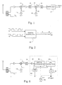
- Fig. 1 presents a conventional procedure for reducing the frequency of a received radio frequency signal.
- the received signal f RX is carried through an antenna filter, a duplex filter when in a radio phone, and an amplifier to a multiplier 11.
- the intermediate frequency f IF1 it would be preferable to select the intermediate frequency f IF1 to be small enough, but in radio apparatus currently used this cannot be done.
- the input signal generally contains also such frequencies with which the other difference frequencies f RX - f LO produced in the multiplier would pass onto the critical frequency f IF1 of the filter and would generate spurious response.
- f IF1 is in the upper half of the received frequency range.
- f IF1 must be greater than the RX band, i.e. it should be typically 35-100 MHz. This is still a far too high a frequency for implementing the detection, and for that purpose, the frequency is again reduced.
- the entire selectivity required of a receiver is implemented with f IF1 , so that almost the only objective of the second mixing is the reduction of the frequency to be detected.
- a method of shifting a signal to another intermediate frequency known in the art is also shown in Figure. 1.
- a first intermediate signal f IF1 and a second local oscillator signal f LO2 received from a second local oscillator LO2 are multiplied in multiplier 14, and the desired mixing result f IF2 is selected with filter 15 of the frequency domain.
- the detection of the modulation is illustrated with a quadrature detector known in the art
- the greatest drawback of the design known in the art is the filter required after the multiplier, which using the prior art techniques cannot be integrated on one and same silicon chip, for instance together with the multiplier and the detector.
- the second drawback is the continuous power consumption of the linear multiplier.
- Patents Abstracts of Japan, vol. 12, no. 500 describes a circuit for generating a difference frequency signal between a pair of input signals, one of the input signals being modulated and the other being unmodulated.
- the modulated input signal is applied to the input (D) of a D-type flip-flop whilst the unmodulated input signal is applied to the clock input (CK) of the flip-flop.
- the output signal (Q) of the flip-flop provides the difference signal.
- FR-A-2451661 and DE-A-3130177 describe similar difference frequency generating circuits.
- a method for producing a frequency difference signal between a modulated signal (f 1 ) and an unmodulated signal (f 2 ) and for detecting the modulation from the frequency difference signal comprising the step of monitoring the time-related order of arrival of the front edges of the pulses of the modulated and unmodulated signal, characterised by the steps of:
- a circuit for downmixing a modulated signal and for detecting information conveyed by the modulation having:
- Embodiments of the present invention have the advantage that the coupling arrangement can be fabricated on a single semiconductor chip. Furthermore, direct detection of the modulating signal is possible at the same time as performing the down converting.
- the selection of the output signal is so accomplished that the front edges of the pulses become synchronized to conform to the modulation containing signal.
- the above formulae are valid when no frequency or phase shift takes place in the input frequencies.
- N (1 + ⁇ ) f 2 f 1 - f 2
- INT ⁇ N(x) is the solution of equality (3) reduced to an integer.
- Fig. 2 presents in highly reduced form the basic idea of the invention.
- the information contained therein is located in a location of the edges of the pulse, to be more precise, in the changes of the front edges thereof.
- the signal f 1 is modulated by a 90 degree phase shift, i.e. the phase is shifted onwards by a length of 0.25 sequence, Fig. 3A.
- the output signal after the point of time t 0 , would have a subsequent edge after 99 sequences, as described above.
- the location of the edge changes and the new location of the edge is provided as solution from the inequality (2) as presented above: N f 2 > N + 1 + ⁇ f 1
- phase modulation in signal f 1 thus results in the output signal a relative phase shift of equal size in the form of sequence lengths, that is, 0.25 in the present instance.
- the relative phase shift located in the input frequency shifts directly, to form a relative phase shift of equal magnitude, into the mixing result.
- the number N is, however, a positive integer, respectively
- INT ⁇ N(x) ⁇ refers to the solution of formula (3) reduced into an integer.
- the relative frequency f 1 of the modulated input signal is 3 and the relative frequency f 2 of the unmodulated mixing signal is 2.
- the broken line 311 shows, as a demonstration, part of the input signal f 1 in a case that no modulation would had taken place.
- the size ⁇ of the modulating phase step is here also 0.25 of the sequence length as the reference numeral 38 refers.
- the broken line represents the input signal f 1 in an instance in which no phase modulation had taken place.
- the phase and frequency separation capacity of the downmixing method is limited and that the essential source of errors, as regards the method, is the detection of the pulse edge by means of the whole sequences either too early or too late.
- the frequencies f 1 and f 2 can be so selected that the defective or missing pulse edges can be localized and either rejected or corrected afterwards, for instance so that the point of time of the pulse edges in a desired time window is stored in the memory.
- the sequence length of an output signal produced as a result of the downmixing can be measured in conjunction with the downmixing illustrated for the detection by measuring the relative location of the pulse edges of the output signal with respect to the pulse edges of a fixed mixing frequency f 2 .
- ⁇ T 1 is the time interval of the pulse edges of f 1 and f 2 when the pulses reach each other again.
- the measurement method of said short periods is known in the art and one of the methods for measuring ⁇ T 1 and ⁇ T 2 is disclosed in patent application FI-896267.
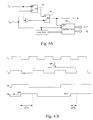
- the downmixing using digital pulse selection according to the invention can be accomplished advantageously by means of a coupling including logical gates as those shown in Fig. 4A.
- the pulse diagram of the coupling is presented in Fig. 4B. From an unmodulated input signal f 2 conducted to data input D samples are taken by means of D flip-flop 43 controlled by a modulated input signal 42 carried to the clock input, whereby the output of the D flip-flop shifts its state every time at the pulse edge of a modulated signal.
- the ascending edge of a pulse is shown in the output whenever the front edge of the signal reaches the clock signal.
- a known drawback of the coupling is only the growth of the delay of the D flip-flop 43 when the ascending edges of the clock and data inputs approach to a distance of only pico-seconds from each other.
- the output is triggered on the decaying edge of f 1 by one half sequence length later with another D flip-flop 44.
- the coupling is reliable in operation even if the input signals were highly asymmetric.
- interpolator 46 If one wants to measure the time intervals ⁇ T 1 and ⁇ T 2 for an detection, it is accomplished with interpolator 46 so that the ascending edge 490 of the output signal, presented in Fig. 4B by line 48, starts the interpolator 46 by calculating the fractions of the sequence length and the subsequent ascending edge of frequency f 2 stops it, whereafter the interpolator starts the calculation of the whole pulses of the control part 47, permitted by f 2 , until a subsequent acceptable pulse edge 491 of difference frequency enters the interpolator and starts the measurement of fraction ⁇ T 2 of the sequence length and discontinuing the counting of the number N of the whole pulses.
- Said interpolator is known in the art, and one such is described in patent application FI-896267.
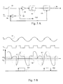
- Fig. 5A presents a second embodiment of the downmixer, and Fig. 5B the pulse diagram thereof. Since the unmodulated mixing frequency f 2 is already of logical level in the form of point frequency, it is preferable to use a solution reverse in embodiment, in which the sampling is controlled with the aid of an unmodulated mixing frequency and in which the location of the pulse edge is determined by the amplification of the amplifier chain 52 and by the level of comparison of comparator 53.
- a relative change of location of the edge of the output signal 54 compared with a preceding one is determined by a change in the edge of the modulated input signal 51 because during the interval between the pulses 541, 542, the amplification of the amplifier chain 52, the amplitude of the modulated input signal 51 and the level of comparison of the comparator remain constant.
- the amplifier 52 may also be an integrator or a derivator, or an amplifier controlled automatically according to the level (e.g. AGC amplifier).
- the function of the logical block 55 is to select the signal for the output signal from each sampling interval in which a change either in a positive or negative direction occurs first.
- FIG. 5A functions so that the ascending edge of the output signal 54 is conceivable only when a signal entering the comparator exceeds the triggering threshold of the comparator in the course of the positive sequence of the clock signal f 2 , in Figure. 5B illustrated by points 57.
- the level of the desired signal need not be amplified into a continuous, logical level pulse sequence, instead, only the local frequency f 2 and the output pulse 54 of the circuit would be of logical level.
- the power consumption of the circuit shown in Fig. 5A and radio frequency interferences caused by logical level signals are reduced to be as small as possible.
- the coupling of the invention With the coupling of the invention, a remarkable saving can be achieved in the power consumption of a radio frequency device. Since in the radio systems, the greatest frequency deviation of the frequency modulation and in the phase modulations, the greatest phase shift speed are quantities known in the art, the operation of the downmixer can after each change in the state be discontinued for so long that the entry of a new change of state, that is, of an information containing edge of the output signal is again potential. Therefore, the active operating time of the mixer can be made short in duration and the power consumption reduced to a fraction of the power consumption of a continuous-operating mixer.
- t e 2.18 ⁇ s, or 97 pcs of f 2 frequency pulses are obtained.
- 97 pulses it is often more preferable to keep logical level calculators operating at f 2 frequency in operation than the pulse processing designs amplifying and comparing the modulated signal, the power consumption whereof being much greater than the logic operating at the same frequency.
- the downmixing of the present invention leads to an FM/PM receiver structure advantageous with a view of the filtering of the frequency domain, and employing only one intermediate frequency, shown in Fig. 6.
- a first intermediate frequency f IF1 is produced similarly as in Fig. 1, but thereafter the signal with f IF1 frequency is amplified with an amplifier 61 for making feasible the logical level signal processing, the digital downmixing according to the principle described in the foregoing is carried out in means 62 and combined therewith, the detection of FM or PM modulation in detector 63 based on pulse time interval measurement.
- an detection 65 of the strength of the entering signal has been added and conversion of the modulation detected in digital form into analog voltage by an analog / digital converter 66.
- the comparison of Figs 1 and 2 shows clearly the advantages achieved with the invention.
- the main source of errors is the timing of the pulse edge of the output signal occurring earlier or later by the amount of one or more whole sequences than what the proper location would be. It is possible to show that this is equivalent to the natural noisiness of the signal and that the signal noise ratio of the detected signal deteriorates for that reason only insignificantly.
- the downmixing principle described above is, in fact, equivalent to the downmixing based on analog multiplication, only with the difference, that selecting a right output signal is carried out by selection in time level and not by filtering the frequency domain as in using an analog multiplier.
- the design according to the method described above is simple to carry out in the form of an integrated circuit and is therefore non-costly.
- the only drawback of the method is that the frequency band of the input signals must be limited.
- the method can be advantageously used for instance to detect the digital modulation in the radio phone system or in the coaxial cable system so that the downmixing is carried out based on pulse selection, and the actual detection based on the measurement of the time interval of the pulses obtained as a result.
- the invention is particularly advantageous to carry out using a logic in which the signal levels are very low.
Landscapes
- Engineering & Computer Science (AREA)
- Power Engineering (AREA)
- Digital Transmission Methods That Use Modulated Carrier Waves (AREA)
- Superheterodyne Receivers (AREA)
- Measuring Frequencies, Analyzing Spectra (AREA)
Claims (11)
- Procédé pour produire un signal de différence de fréquence entre un signal modulé (f1) et un signal non modulé (f2) et pour détecter la modulation à partir du signal de différence de fréquence, le procédé comprenant l'étape consistant à suivre l'ordre d'arrivée dans le temps des fronts avant des impulsions du signal modulé et non modulé, caractérisé par les étapes :de production d'un front avant d'une impulsion de signal de différence de fréquence au même instant que le front avant d'une impulsion de signal modulé pour lequel on trouve que l'ordre d'arrivée dans le temps des fronts d'impulsions du signal modulé (f1) et du signal non modulé (f2) varie, de sorte que le décalage de fréquence ou le déphasage du signal modulé peut être détecté sous la forme d'une variation correspondante du signal de différence de fréquence ; etde détection de la modulation du signal de différence de fréquence sur la base des positions des fronts d'impulsions du signal de différence de fréquence.
- Procédé selon la revendication 1, dans lequel le signal de différence de fréquence est produit en prélevant des échantillons commandés par le signal (f1) modulé à partir d'une fréquence (f2) non modulée et en sélectionnant un premier échantillon de signe inversé pour la sortie.
- Procédé selon la revendication 1 ou 2, dans lequel, pour le front d'impulsion avant du signal de différence de fréquence, le front d'impulsion avant du signal (f1) d'entrée modulé est sélectionné et est le plus proche dans le temps du front avant respectif d'un signal (f2) non modulé.
- Procédé selon l'une quelconque des revendications précédentes, dans lequel la longueur de séquence du signal de différence de fréquence varie, la position relative des fronts d'impulsions du signal de différence de fréquence est mesurée par rapport aux fronts d'impulsions d'un signal (f2) non modulé et la longueur (tc) de séquence est calculée à partir de la formule suivante :
- Circuit pour mélanger-abaisser un signal modulé et pour détecter les informations contenues dans la modulation, le circuit ayant :caractérisé par des moyens destinés à synchroniser le front avant d'une impulsion et du signal de différence avec le front avant d'une impulsion d'un premier signal à haute fréquence.une première entrée pour recevoir un premier signal (f1) à haute fréquence modulé en fréquence ou en phase ;une seconde entrée pour recevoir un second signal (f2) à haute fréquence, ce second signal étant non modulé ;une sortie sur laquelle est fournie un signal (fOUT) de différence contenant des informations de modulation desdites fréquences ;des moyens pour observer l'ordre d'arrivée dans le temps des fronts avant des impulsions des premier et second signaux à haute fréquence et pour fournir un front avant d'impulsion au signal de différence chaque fois que l'ordre d'arrivée des fronts avant desdites impulsions de signal d'entrée varie,
- Circuit selon la revendication 5, dans lequel les moyens d'observation, de fourniture et de synchronisation sont constitués d'une bascule (43) de type D à l'entrée d'horloge de laquelle est fourni le premier signal (f1) à haute fréquence et à l'entrée de données de laquelle est fourni le second signal (f2) à haute fréquence, et à la sortie de laquelle on obtient ledit signal de différence.
- Circuit selon la revendication 6, comprenant une seconde bascule (44) de type D dont l'entrée d'horloge est fonctionnellement connectée à ladite première entrée du circuit, l'entrée de données de la seconde bascule de type D étant connectée à la sortie de la première bascule de type D (43), et la sortie de la seconde bascule de type D fournissant un second signal de différence.
- Circuit selon la revendication 7, caractérisé en ce que le circuit comprend un interpolateur (46) comptant les fractions de la longueur de séquence, les entrées de l'interpolateur comprenant ledit second signal de différence et ledit second signal à haute fréquence (f2), et étant agencées de façon à calculer la distance T1 dans le temps du front avant d'une impulsion de sortie détectée par rapport au front d'impulsion d'un signal (f2) non modulé suivant, la distance T2 dans le temps d'une impulsion de sortie détectée suivante par rapport au front d'impulsion d'un signal (f2) non modulé suivant, et le nombre M de séquences entières du signal non modulé restant entre lesdits fronts d'impulsions, de sorte que la longueur de séquence tc du signal de différence de fréquence peut être calculée à partir de la formule suivante :
- Circuit selon la revendication 5, comprenant :un premier commutateur (S1), des moyens (52) amplificateurs, un comparateur (53) et des moyens (55) logiques, tous couplés en aval dudit premier commutateur, de sorte que ledit premier signal peut être connecté par l'intermédiaire dudit premier commutateur (S1) à l'entrée des moyens (52) amplificateurs, et que ledit signal de différence peut être fourni à partir de la sortie des moyens logiques, etun second commutateur (S2) par l'intermédiaire duquel le signal d'entrée (f1) des moyens amplificateurs peut être directement connecté aux moyens logiques (55),la position des premier et second commutateurs à un instant quelconque étant déterminée sous la forme d'une réponse audit second signal (f2), de sorte que des échantillons provenant du premier signal sont acheminés aux moyens amplificateurs.
- Circuit selon la revendication 9, dans lequel les moyens logiques ne fournissent ledit signal de différence avec un front montant que lorsqu'un signal atteignant le comparateur (53) dépasse le seuil de déclenchement du comparateur au cours de la séquence positive du premier signal (f1).
- Circuit selon l'une quelconque des revendications 5 à 10, dans lequel, à l'exception d'une fréquence d'horloge de base du circuit, toutes les activités sont interrompues, à partir du moment où le front d'impulsion détecté se situe à la fréquence de différence, pendant un temps dépendant de la largeur de bande du signal modulé, et dans lequel, après ladite période de temps, un nouveau front d'impulsion est probable à la fréquence de différence.
Applications Claiming Priority (2)
| Application Number | Priority Date | Filing Date | Title |
|---|---|---|---|
| FI930973 | 1993-03-04 | ||
| FI930973A FI96809C (fi) | 1993-03-04 | 1993-03-04 | Menetelmä ja kytkentäjärjestely kahden signaalitaajuuden erotuksen muodostamiseksi ja modulaation ilmaisemiseksi |
Publications (2)
| Publication Number | Publication Date |
|---|---|
| EP0614268A1 EP0614268A1 (fr) | 1994-09-07 |
| EP0614268B1 true EP0614268B1 (fr) | 1998-12-16 |
Family
ID=8537500
Family Applications (1)
| Application Number | Title | Priority Date | Filing Date |
|---|---|---|---|
| EP94301331A Expired - Lifetime EP0614268B1 (fr) | 1993-03-04 | 1994-02-24 | Procédé et appareil pour produire un signal de différence entre fréquences de signal et pour la détection de modulation |
Country Status (4)
| Country | Link |
|---|---|
| EP (1) | EP0614268B1 (fr) |
| JP (1) | JPH06326629A (fr) |
| DE (1) | DE69415188T2 (fr) |
| FI (1) | FI96809C (fr) |
Family Cites Families (3)
| Publication number | Priority date | Publication date | Assignee | Title |
|---|---|---|---|---|
| DE2909921A1 (de) * | 1979-03-14 | 1980-09-25 | Itt Ind Gmbh Deutsche | Tonkanalschaltung bei frequenzmodulierten signalen |
| DE3130177A1 (de) * | 1981-07-30 | 1983-02-17 | Siemens AG, 1000 Berlin und 8000 München | Digitaler frequenzmischer |
| JPS63211915A (ja) * | 1987-02-27 | 1988-09-05 | Fujitsu Ten Ltd | 周波数変換回路 |
-
1993
- 1993-03-04 FI FI930973A patent/FI96809C/fi active
-
1994
- 1994-02-24 DE DE69415188T patent/DE69415188T2/de not_active Expired - Fee Related
- 1994-02-24 EP EP94301331A patent/EP0614268B1/fr not_active Expired - Lifetime
- 1994-03-04 JP JP6034697A patent/JPH06326629A/ja active Pending
Also Published As
| Publication number | Publication date |
|---|---|
| FI96809C (fi) | 1996-08-26 |
| FI930973L (fi) | 1994-09-05 |
| JPH06326629A (ja) | 1994-11-25 |
| EP0614268A1 (fr) | 1994-09-07 |
| FI930973A0 (fi) | 1993-03-04 |
| FI96809B (fi) | 1996-05-15 |
| DE69415188D1 (de) | 1999-01-28 |
| DE69415188T2 (de) | 1999-07-08 |
Similar Documents
| Publication | Publication Date | Title |
|---|---|---|
| US5640428A (en) | Direct conversion receiver | |
| US7496158B2 (en) | Swept bandpass filter frequency modulated continuous wave (FMCW) receiver and related method | |
| JPH0129469B2 (fr) | ||
| AU610440B2 (en) | Multiple radio frequency single receiver radar operation | |
| EP0199448B1 (fr) | Appareil déterminant les erreurs de phase et de fréquence | |
| US6664919B2 (en) | Radar device | |
| EP0106029A1 (fr) | Méthode et appareil pour mesurer l'amplitude d'un signal périodique parasité sans référence de phase | |
| US5757868A (en) | Digital phase detector with integrated phase detection | |
| JP4195239B2 (ja) | ジッタ測定装置 | |
| EP0998084B1 (fr) | Démodulateur et procédé de démodulation de signaux MDP qui employent une technique de fenêtrage de la largeur de la période | |
| US5732108A (en) | Method and apparatus for producing a difference signal between two signal frequencies, and for detection of modulation | |
| EP0614268A1 (fr) | Procédé et appareil pour produire un signal de différence entre signaux de fréquence et pour la détection de modulation | |
| US5424738A (en) | Analog-digital encoding circuit with automatic compensation for the zero offset | |
| US6819723B1 (en) | Digital FM demodulator with reduced quantization noise | |
| GB977474A (en) | Tone frequency control means for keyed filtered systems | |
| US20050129149A1 (en) | Detecting GSM downlink signal frequency correction burst | |
| RU2106655C1 (ru) | Частотно-модулированный высотомер | |
| US4864221A (en) | Filter, phase-measuring device and method for application of said filter | |
| US7317768B2 (en) | Demodulator and demodulation method for demodulating received signals | |
| RU2133483C1 (ru) | Частотно-модулированный высотомер | |
| EP1022847A2 (fr) | FM démodulateur | |
| GB2213026A (en) | Control arrangement for a phase shift keying system | |
| SU1215188A1 (ru) | Устройство дл приема фазоманипулированных сигналов | |
| JPH06294829A (ja) | 周波数測定装置 | |
| JPS595874B2 (ja) | シンゴウケンシユツカイロ |
Legal Events
| Date | Code | Title | Description |
|---|---|---|---|
| PUAI | Public reference made under article 153(3) epc to a published international application that has entered the european phase |
Free format text: ORIGINAL CODE: 0009012 |
|
| AK | Designated contracting states |
Kind code of ref document: A1 Designated state(s): DE FR GB SE |
|
| 17P | Request for examination filed |
Effective date: 19950307 |
|
| 17Q | First examination report despatched |
Effective date: 19970718 |
|
| RAP1 | Party data changed (applicant data changed or rights of an application transferred) |
Owner name: NOKIA MOBILE PHONES LTD. |
|
| GRAG | Despatch of communication of intention to grant |
Free format text: ORIGINAL CODE: EPIDOS AGRA |
|
| GRAG | Despatch of communication of intention to grant |
Free format text: ORIGINAL CODE: EPIDOS AGRA |
|
| GRAH | Despatch of communication of intention to grant a patent |
Free format text: ORIGINAL CODE: EPIDOS IGRA |
|
| GRAH | Despatch of communication of intention to grant a patent |
Free format text: ORIGINAL CODE: EPIDOS IGRA |
|
| GRAA | (expected) grant |
Free format text: ORIGINAL CODE: 0009210 |
|
| AK | Designated contracting states |
Kind code of ref document: B1 Designated state(s): DE FR GB SE |
|
| REF | Corresponds to: |
Ref document number: 69415188 Country of ref document: DE Date of ref document: 19990128 |
|
| ET | Fr: translation filed | ||
| PG25 | Lapsed in a contracting state [announced via postgrant information from national office to epo] |
Ref country code: SE Free format text: LAPSE BECAUSE OF FAILURE TO SUBMIT A TRANSLATION OF THE DESCRIPTION OR TO PAY THE FEE WITHIN THE PRESCRIBED TIME-LIMIT Effective date: 19990316 |
|
| PLBE | No opposition filed within time limit |
Free format text: ORIGINAL CODE: 0009261 |
|
| STAA | Information on the status of an ep patent application or granted ep patent |
Free format text: STATUS: NO OPPOSITION FILED WITHIN TIME LIMIT |
|
| 26N | No opposition filed | ||
| REG | Reference to a national code |
Ref country code: GB Ref legal event code: IF02 |
|
| PGFP | Annual fee paid to national office [announced via postgrant information from national office to epo] |
Ref country code: FR Payment date: 20020212 Year of fee payment: 9 |
|
| PGFP | Annual fee paid to national office [announced via postgrant information from national office to epo] |
Ref country code: GB Payment date: 20020227 Year of fee payment: 9 |
|
| PGFP | Annual fee paid to national office [announced via postgrant information from national office to epo] |
Ref country code: DE Payment date: 20020314 Year of fee payment: 9 |
|
| REG | Reference to a national code |
Ref country code: GB Ref legal event code: 732E |
|
| PG25 | Lapsed in a contracting state [announced via postgrant information from national office to epo] |
Ref country code: GB Free format text: LAPSE BECAUSE OF NON-PAYMENT OF DUE FEES Effective date: 20030224 |
|
| PG25 | Lapsed in a contracting state [announced via postgrant information from national office to epo] |
Ref country code: DE Free format text: LAPSE BECAUSE OF NON-PAYMENT OF DUE FEES Effective date: 20030902 |
|
| GBPC | Gb: european patent ceased through non-payment of renewal fee | ||
| PG25 | Lapsed in a contracting state [announced via postgrant information from national office to epo] |
Ref country code: FR Free format text: LAPSE BECAUSE OF NON-PAYMENT OF DUE FEES Effective date: 20031031 |
|
| REG | Reference to a national code |
Ref country code: FR Ref legal event code: ST |