EP0616360A2 - Vorrichtung und Verfahren um Halbleiterscheiben zu Kühlen - Google Patents
Vorrichtung und Verfahren um Halbleiterscheiben zu Kühlen Download PDFInfo
- Publication number
- EP0616360A2 EP0616360A2 EP94104187A EP94104187A EP0616360A2 EP 0616360 A2 EP0616360 A2 EP 0616360A2 EP 94104187 A EP94104187 A EP 94104187A EP 94104187 A EP94104187 A EP 94104187A EP 0616360 A2 EP0616360 A2 EP 0616360A2
- Authority
- EP
- European Patent Office
- Prior art keywords
- wafer
- pedestal
- cooling
- cooling surface
- electrostatic chuck
- Prior art date
- Legal status (The legal status is an assumption and is not a legal conclusion. Google has not performed a legal analysis and makes no representation as to the accuracy of the status listed.)
- Ceased
Links
Images

Classifications
-
- H—ELECTRICITY
- H10—SEMICONDUCTOR DEVICES; ELECTRIC SOLID-STATE DEVICES NOT OTHERWISE PROVIDED FOR
- H10P—GENERIC PROCESSES OR APPARATUS FOR THE MANUFACTURE OR TREATMENT OF DEVICES COVERED BY CLASS H10
- H10P72/00—Handling or holding of wafers, substrates or devices during manufacture or treatment thereof
- H10P72/04—Apparatus for manufacture or treatment
- H10P72/0431—Apparatus for thermal treatment
- H10P72/0432—Apparatus for thermal treatment mainly by conduction
-
- H—ELECTRICITY
- H10—SEMICONDUCTOR DEVICES; ELECTRIC SOLID-STATE DEVICES NOT OTHERWISE PROVIDED FOR
- H10P—GENERIC PROCESSES OR APPARATUS FOR THE MANUFACTURE OR TREATMENT OF DEVICES COVERED BY CLASS H10
- H10P72/00—Handling or holding of wafers, substrates or devices during manufacture or treatment thereof
- H10P72/04—Apparatus for manufacture or treatment
- H10P72/0431—Apparatus for thermal treatment
- H10P72/0434—Apparatus for thermal treatment mainly by convection
-
- H—ELECTRICITY
- H10—SEMICONDUCTOR DEVICES; ELECTRIC SOLID-STATE DEVICES NOT OTHERWISE PROVIDED FOR
- H10P—GENERIC PROCESSES OR APPARATUS FOR THE MANUFACTURE OR TREATMENT OF DEVICES COVERED BY CLASS H10
- H10P72/00—Handling or holding of wafers, substrates or devices during manufacture or treatment thereof
- H10P72/06—Apparatus for monitoring, sorting, marking, testing or measuring
- H10P72/0602—Temperature monitoring
-
- H—ELECTRICITY
- H10—SEMICONDUCTOR DEVICES; ELECTRIC SOLID-STATE DEVICES NOT OTHERWISE PROVIDED FOR
- H10P—GENERIC PROCESSES OR APPARATUS FOR THE MANUFACTURE OR TREATMENT OF DEVICES COVERED BY CLASS H10
- H10P95/00—Generic processes or apparatus for manufacture or treatments not covered by the other groups of this subclass
- H10P95/90—Thermal treatments, e.g. annealing or sintering
Definitions
- the present invention relates to the manufacture of integrated circuits. More particularly, the present invention relates to the cooling of semiconductor wafers during the manufacture of integrated circuits.
- Intense heat is often used during the various process steps that are necessary to fabricate integrated circuits on silicon wafers. It is then necessary to cool the wafers because the wafer temperature is usually in the range of 500°C to 800°C after such processing steps, making transport difficult (e.g. in a standard plastic wafer carrier), and limiting the ability to perform subsequent processing steps that may require lower wafer temperatures.
- the wafer cools rapidly by radiation, i.e. by thermal transfer to the ambient.
- the rate at which the wafer cools by radiation slows considerably.
- the wafer cooling rate slows because the rate of cooling by radiation is proportional to the wafer temperature raised to the fourth power. That is, the amount of decrease in the rate at which the wafer cools by radiation becomes greater as the wafer temperature decreases.
- the present invention provides an improved method and apparatus for rapidly cooling a processed wafer under vacuum without contaminating the wafer.
- a water cooled pedestal includes an upper, wafer cooling surface, a small portion of which is an electrostatic chuck formed of a ceramic material, and another, larger portion of which is a thermally conductive metal portion. Both the ceramic portion and the metal portion of the pedestal have the same profile and are finished with a precision mirror finish to allow intimate contact between the wafer and the water cooled pedestal surface, and thus provide enhanced thermal transfer from the wafer to the water cooled pedestal to expedite wafer cooling.
- the present invention therefore includes an electrostatic chuck which retains a wafer to the water cooled pedestal, thereby eliminating the need to incorporate a wafer clamp into the cooling chamber design.
- the present invention also includes a pedestal having a significant portion of the pedestal wafer cooling surface formed of a thermally conductive material, which thus allows rapid wafer cooling.
- the highly polished pedestal surface maximizes wafer to pedestal contact and therefore provides optimal thermal transfer from the wafer to the water cooled pedestal, obviating the need to circulate a thermal transfer medium, such as argon or other inert gases, between the wafer and the water cooled pedestal.
- the present invention is an improved method and apparatus for cooling wafers.
- the invention provides a wafer cooling pedestal having a wafer cooling surface which includes both an electrostatic chuck portion to hold the wafer to the pedestal and a thermal transfer portion to cool the wafer.
- the wafer cooling surface of the pedestal is mirror finished to provide intimate contact between the pedestal and the wafer, thereby obviating the need for a thermal transfer medium, such as argon or other inert gas, between the wafer and the pedestal.
- Fig. 1a is a plan view
- Fig. 1b is a sectional side view of a portion of a wafer cooling apparatus that includes an improved pedestal according to a preferred embodiment of the present invention.
- a processed (and therefore "hot") wafer 16 is transferred into a cooling chamber 11.
- a lifter 13 in the chamber picks up the processed wafer and positions the wafer on a water cooled pedestal 14.
- the lifter may be of any type known in the art and it is not critical to the operation or understanding of the present invention.
- the water cooled pedestal is primarily composed of the metal aluminum or alloys thereof because of its high metallic heat conductivity. It includes a cooling surface 15, a portion of which incorporates an electrostatic chuck 12 which holds the wafer to the pedestal by means of an electrostatic charge on the pedestal surface. After the processed wafer is placed on the water cooled pedestal, power is applied to the electrostatic chuck to generate the electrostatic charge that holds the processed wafer to the water cooled pedestal.
- Fig. 1a The embodiment of the invention depicted in Fig. 1a provides three separate points at which the chuck 12 holds the wafer 16 to the water cooled pedestal 14.
- the electrostatic chuck 12 occupies a small portion of the total available wafer cooling surface 15 of the water cooled pedestal 14.
- the invention provides an electrostatic chuck which serves to secure the wafer to a cooling surface and which is configured to occupy a minimal amount of the cooling surface, such that thermal transfer is not unnecessarily inhibited by interference from the typically thermally insulating electrostatic chuck.
- the electrostatic chuck by drawing the wafer to the cooling surface of the pedestal and increasing contact between the wafer and the cooling surface of the pedestal, improves thermal transfer between the wafer and the pedestal without blocking thermal transfer across a large portion of the cooling surface. Additionally, the material from which the electrostatic chuck of the present invention is formed does not have to be thermally conductive, nor does the chuck need to be thin. The present invention thus allows an electrostatic chuck that withstands high voltages, because the insulating layer may be made from any desired material and it may be as thick as necessary to withstand such voltages without degrading thermal transfer between the wafer and the pedestal.
- the present invention may be practiced with any configuration and combination of electrostatic chucks on cooling surface as required by the application to which the invention is put.
- a preferred embodiment of the invention is shown in Fig. 1a, in which three portions of the cooling surface 15 of the water cooled pedestal 14 are provided for electrostatic attachment to retain the wafer to the pedestal.
- Other embodiments of the invention may provide more or fewer points of electrostatic attachment, and such points of attachment need not be rectangular as shown in Fig. 1a, but may be round, square, triangular, annular, etc.
- a power line 19 is provided for supplying electrical energy to the electrostatic chuck 12 and thereby maintain the wafer in intimate contact with the cooling surface of the water cooled pedestal as desired. That is, electrical energy is supplied to the chuck to secure the wafer to the pedestal cooling surface, and the supply of electrical energy is turned off to allow the wafer to be removed from or positioned on the pedestal wafer cooling surface.
- the supply of electrical current may be controlled by any of the various known means.
- a water supply conduit 17 allows continuous circulation of water (or other cooling medium if desired) within the aluminum pedestal to draw heat from the pedestal as the heat is transferred to the pedestal from the processed wafer. Both the water supply conduit and the power line are located under the pedestal such that the cooling chamber may be maintained under vacuum. It will be appreciated that the pedestal of Fig. 1 is shown for purposes of example. The present invention finds ready application in any type of wafer cooling pedestal, including those pedestals that do not rely on circulation of a cooling medium within the pedestal, etc.
- the wafer contacting surface of the electrostatic chuck is at exactly the same height as the rest of the cooling surface of the water cooled pedestal.
- an extremely flat surface is provided which serves to increase the actual contact area between the processed wafer and the water cooled pedestal.
- both the cooling surface of the water cooled pedestal and the wafer contacting surface of the electrostatic chuck have a mirror surface finish to further increase actual contact area between the wafer and the cooling surface of the water cooled pedestal.
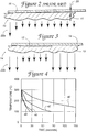
- Fig. 2 is a schematic diagram showing prior art wafer-to-pedestal heat transfer where wafer contour and pedestal surface mismatch occur. It is known that in most wafer cooling applications, the actual area of contact between a wafer and a pedestal is quite small, i.e. on the order of 2-3%. This surface-to-surface mismatch, and the corresponding lack of intimate contact between the wafer and the water cooled pedestal, occur because the processed wafer does have an exact flat and parallel surface relative to that of the water cooled pedestal. This is especially true after the wafer has been subjected to high temperature processing., when the wafer may be curved, warped, or bowed as shown in Fig. 2.
- This distortion in the planarity of the wafer creates gaps (shown as arrows 20 in Fig. 2) between the wafer 16 and the cooling surface 15 of the water cooled pedestal 14. Having such a gap between the wafer and the cooling surface of the pedestal in a vacuum chamber, where the vacuum acts as a thermal insulator, makes it very difficult to transfer heat from the wafer to the pedestal. This is why known approaches to cooling wafers use a thermal transfer medium, such as argon or other inert gas, in the gaps between the wafer and the pedestal to improve thermal transfer from the wafer to the pedestal and thus speed up the wafer cooling process.
- a thermal transfer medium such as argon or other inert gas
- FIG. 2 A heat transfer profile, consisting of lines with arrows 22a, is shown in Fig. 2 in which the longer lines indicate increased thermal transfer at the point where the wafer is in intimate contact with the cooling surface of the aluminum pedestal, and in which the shorter lines indicate decreased thermal transfer where there is a gap between the wafer and the cooling surface of the pedestal.
- Fig. 3 is a schematic diagram showing wafer-to-pedestal heat transfer according to a preferred embodiment of the present invention.
- an electrostatic chuck 12 is used to draw the wafer to the cooling surface 15 of the pedestal 14.
- the electrostatic charge induced by the chuck forces the wafer to comply to the profile of the cooling surface of the pedestal and thus increases the actual contact area between the wafer and the water cooled pedestal.
- the present invention exploits the advantages of the electrostatic chuck to improve wafer contact with a pedestal cooling surface, and thereby obviates the need for a thermal transfer medium. Additionally, the present invention minimizes the total surface area of the electrostatic chuck and maximizes the cooling surface, thereby providing maximum thermal transfer from the wafer to the pedestal.
- a heat transfer profile consisting of lines with arrows 22b, is shown in Fig. 3 in which the longer lines indicate increased thermal transfer at the point where the wafer is in intimate contact with the cooling surface 15 of the pedestal, and in which the shorter lines indicate decreased thermal transfer where the wafer contacts the electrostatic chuck 12.
- Fig. 4 is a graph showing a wafer cooling profile for prior art wafer cooling techniques and for wafer cooling in accordance with the present invention.
- a first line 40 plots a wafer cooling curve (cooling time in seconds vs. cooling temperature in °C) in which a wafer is cooled, in the absence of a thermal transfer medium, on a pedestal having a precision surface finish.
- Such finish is described in terms of surface roughness (R a ), which is the average deviation of the surface above and below a hypothetical flat plane per unit of length.
- surface roughness R a shall express length in unit terms of 2.5 X 10 ⁇ 5 mm (10 ⁇ 6 inches) .
- known polishing techniques are used to obtain the values of surface roughness expressed in the example.
- Line 40 in Fig. 4 plots wafer cooling on a pedestal having a precision 25 R a finish. It can be seen from the figure, that for such trial, the wafer cooling speed is very slow.
- a second line 44 plots a wafer cooling curve in which a wafer is cooled in the presence of a thermal transfer medium on a pedestal having a surface with a 25 R a finish.
- a third line 42 plots a wafer cooling curve in which a wafer is cooled in the absence of a thermal transfer medium on a pedestal having a surface with a 25 R a finish and which includes an electrostatic chuck, i.e. an electrostatic chuck of the type known in which the chuck includes the entire surface of the pedestal. It can be seen that an electrostatic chuck provides some improvement over a pedestal that is used to cool a wafer in the absence a thermal transfer medium, but that the performance of this configuration is far short of that of the state of the art.
- a fourth line 46 plots a wafer cooling curve in which a wafer is cooled in the absence of a thermal transfer medium on a pedestal having a surface with a 1 R a finish (i.e. mirror finish) and which includes a cooling surface, a portion of which includes an electrostatic chuck, in accordance with the present invention. It can be seen from the figure that the performance of the present invention for wafer cooling substantially approaches that of the state of the art. It is significant to note that because the present invention does not require the thermal transfer medium, such as an inert gas, which is necessary in state of the art wafer cooling techniques, the invention provides a cleaner cooling process when compared to the existing method.
- the thermal transfer medium such as an inert gas
Landscapes
- Container, Conveyance, Adherence, Positioning, Of Wafer (AREA)
Applications Claiming Priority (2)
| Application Number | Priority Date | Filing Date | Title |
|---|---|---|---|
| US32361 | 1993-03-17 | ||
| US08/032,361 US5345999A (en) | 1993-03-17 | 1993-03-17 | Method and apparatus for cooling semiconductor wafers |
Publications (2)
| Publication Number | Publication Date |
|---|---|
| EP0616360A2 true EP0616360A2 (de) | 1994-09-21 |
| EP0616360A3 EP0616360A3 (de) | 1994-10-19 |
Family
ID=21864555
Family Applications (1)
| Application Number | Title | Priority Date | Filing Date |
|---|---|---|---|
| EP9494104187A Ceased EP0616360A3 (de) | 1993-03-17 | 1994-03-17 | Vorrichtung und Verfahren um Halbleiterscheiben zu Kühlen. |
Country Status (4)
| Country | Link |
|---|---|
| US (1) | US5345999A (de) |
| EP (1) | EP0616360A3 (de) |
| JP (1) | JPH06326181A (de) |
| KR (1) | KR100314573B1 (de) |
Families Citing this family (190)
| Publication number | Priority date | Publication date | Assignee | Title |
|---|---|---|---|---|
| US5486975A (en) * | 1994-01-31 | 1996-01-23 | Applied Materials, Inc. | Corrosion resistant electrostatic chuck |
| US5883778A (en) * | 1994-02-28 | 1999-03-16 | Applied Materials, Inc. | Electrostatic chuck with fluid flow regulator |
| US5548470A (en) * | 1994-07-19 | 1996-08-20 | International Business Machines Corporation | Characterization, modeling, and design of an electrostatic chuck with improved wafer temperature uniformity |
| JP4079992B2 (ja) * | 1994-10-17 | 2008-04-23 | バリアン・セミコンダクター・エクイップメント・アソシエイツ・インコーポレイテッド | 導電性被処理体を載置部材に締め付けるための装置及び静電クランピング方法 |
| US5908504A (en) * | 1995-09-20 | 1999-06-01 | Memc Electronic Materials, Inc. | Method for tuning barrel reactor purge system |
| US6370007B2 (en) | 1995-09-20 | 2002-04-09 | Hitachi, Ltd. | Electrostatic chuck |
| EP0764979A3 (de) | 1995-09-20 | 1998-07-15 | Hitachi, Ltd. | Elektrostatische Anziehungselektrode und Herstellungsverfahren dafür |
| US5746834A (en) * | 1996-01-04 | 1998-05-05 | Memc Electronics Materials, Inc. | Method and apparatus for purging barrel reactors |
| US5810933A (en) * | 1996-02-16 | 1998-09-22 | Novellus Systems, Inc. | Wafer cooling device |
| JP3591977B2 (ja) * | 1996-03-18 | 2004-11-24 | キヤノン株式会社 | マイクロ波プラズマcvd法を用いた膜堆積方法および膜堆積装置 |
| US5837058A (en) * | 1996-07-12 | 1998-11-17 | Applied Materials, Inc. | High temperature susceptor |
| US5708557A (en) * | 1996-08-22 | 1998-01-13 | Packard Hughes Interconnect Company | Puncture-resistant electrostatic chuck with flat surface and method of making the same |
| US6073366A (en) | 1997-07-11 | 2000-06-13 | Asm America, Inc. | Substrate cooling system and method |
| US5969934A (en) * | 1998-04-10 | 1999-10-19 | Varian Semiconductor Equipment Associats, Inc. | Electrostatic wafer clamp having low particulate contamination of wafers |
| JPH11307430A (ja) | 1998-04-23 | 1999-11-05 | Canon Inc | 露光装置およびデバイス製造方法ならびに駆動装置 |
| US6219219B1 (en) | 1998-09-30 | 2001-04-17 | Applied Materials, Inc. | Cathode assembly containing an electrostatic chuck for retaining a wafer in a semiconductor wafer processing system |
| US6217272B1 (en) | 1998-10-01 | 2001-04-17 | Applied Science And Technology, Inc. | In-line sputter deposition system |
| US6328858B1 (en) | 1998-10-01 | 2001-12-11 | Nexx Systems Packaging, Llc | Multi-layer sputter deposition apparatus |
| DE69937255T2 (de) * | 1998-11-20 | 2008-07-03 | Steag RTP Systems, Inc., San Jose | Schnell-aufheiz- und -kühlvorrichtung für halbleiterwafer |
| US6368410B1 (en) * | 1999-06-28 | 2002-04-09 | General Electric Company | Semiconductor processing article |
| US6839217B1 (en) | 1999-10-01 | 2005-01-04 | Varian Semiconductor Equipment Associates, Inc. | Surface structure and method of making, and electrostatic wafer clamp incorporating surface structure |
| US6362946B1 (en) | 1999-11-02 | 2002-03-26 | Varian Semiconductor Equipment Associates, Inc. | Electrostatic wafer clamp having electrostatic seal for retaining gas |
| US6538873B1 (en) | 1999-11-02 | 2003-03-25 | Varian Semiconductor Equipment Associates, Inc. | Active electrostatic seal and electrostatic vacuum pump |
| US6530733B2 (en) | 2000-07-27 | 2003-03-11 | Nexx Systems Packaging, Llc | Substrate processing pallet and related substrate processing method and machine |
| US6682288B2 (en) | 2000-07-27 | 2004-01-27 | Nexx Systems Packaging, Llc | Substrate processing pallet and related substrate processing method and machine |
| US6821912B2 (en) | 2000-07-27 | 2004-11-23 | Nexx Systems Packaging, Llc | Substrate processing pallet and related substrate processing method and machine |
| US7479456B2 (en) | 2004-08-26 | 2009-01-20 | Applied Materials, Inc. | Gasless high voltage high contact force wafer contact-cooling electrostatic chuck |
| US6686598B1 (en) | 2000-09-01 | 2004-02-03 | Varian Semiconductor Equipment Associates, Inc. | Wafer clamping apparatus and method |
| US6951593B2 (en) * | 2001-01-15 | 2005-10-04 | Lintec Corporation | Laminating device and laminating method |
| DE10246282B4 (de) * | 2002-10-02 | 2005-12-29 | Suss Microtec Test Systems Gmbh | Prober zum Testen von Substraten bei tiefen Temperaturen |
| US7100954B2 (en) | 2003-07-11 | 2006-09-05 | Nexx Systems, Inc. | Ultra-thin wafer handling system |
| US7780793B2 (en) * | 2004-02-26 | 2010-08-24 | Applied Materials, Inc. | Passivation layer formation by plasma clean process to reduce native oxide growth |
| US20050230350A1 (en) | 2004-02-26 | 2005-10-20 | Applied Materials, Inc. | In-situ dry clean chamber for front end of line fabrication |
| US7666464B2 (en) | 2004-10-23 | 2010-02-23 | Applied Materials, Inc. | RF measurement feedback control and diagnostics for a plasma immersion ion implantation reactor |
| US20060130971A1 (en) * | 2004-12-21 | 2006-06-22 | Applied Materials, Inc. | Apparatus for generating plasma by RF power |
| JP2010084230A (ja) * | 2008-09-04 | 2010-04-15 | Tokyo Electron Ltd | 成膜装置、基板処理装置及び回転テーブル |
| US9324576B2 (en) | 2010-05-27 | 2016-04-26 | Applied Materials, Inc. | Selective etch for silicon films |
| US10283321B2 (en) | 2011-01-18 | 2019-05-07 | Applied Materials, Inc. | Semiconductor processing system and methods using capacitively coupled plasma |
| US8771539B2 (en) | 2011-02-22 | 2014-07-08 | Applied Materials, Inc. | Remotely-excited fluorine and water vapor etch |
| US8999856B2 (en) | 2011-03-14 | 2015-04-07 | Applied Materials, Inc. | Methods for etch of sin films |
| US9064815B2 (en) | 2011-03-14 | 2015-06-23 | Applied Materials, Inc. | Methods for etch of metal and metal-oxide films |
| US8771536B2 (en) | 2011-08-01 | 2014-07-08 | Applied Materials, Inc. | Dry-etch for silicon-and-carbon-containing films |
| US8679982B2 (en) | 2011-08-26 | 2014-03-25 | Applied Materials, Inc. | Selective suppression of dry-etch rate of materials containing both silicon and oxygen |
| US8679983B2 (en) | 2011-09-01 | 2014-03-25 | Applied Materials, Inc. | Selective suppression of dry-etch rate of materials containing both silicon and nitrogen |
| US8927390B2 (en) | 2011-09-26 | 2015-01-06 | Applied Materials, Inc. | Intrench profile |
| US8808563B2 (en) | 2011-10-07 | 2014-08-19 | Applied Materials, Inc. | Selective etch of silicon by way of metastable hydrogen termination |
| WO2013070436A1 (en) | 2011-11-08 | 2013-05-16 | Applied Materials, Inc. | Methods of reducing substrate dislocation during gapfill processing |
| CN204375716U (zh) * | 2012-03-05 | 2015-06-03 | 应用材料公司 | 遮蔽框、基板支撑件以及等离子体增强型化学气相沉积设备 |
| US9267739B2 (en) | 2012-07-18 | 2016-02-23 | Applied Materials, Inc. | Pedestal with multi-zone temperature control and multiple purge capabilities |
| US9373517B2 (en) | 2012-08-02 | 2016-06-21 | Applied Materials, Inc. | Semiconductor processing with DC assisted RF power for improved control |
| US9034770B2 (en) | 2012-09-17 | 2015-05-19 | Applied Materials, Inc. | Differential silicon oxide etch |
| US9023734B2 (en) | 2012-09-18 | 2015-05-05 | Applied Materials, Inc. | Radical-component oxide etch |
| US9390937B2 (en) | 2012-09-20 | 2016-07-12 | Applied Materials, Inc. | Silicon-carbon-nitride selective etch |
| US9132436B2 (en) | 2012-09-21 | 2015-09-15 | Applied Materials, Inc. | Chemical control features in wafer process equipment |
| US8765574B2 (en) | 2012-11-09 | 2014-07-01 | Applied Materials, Inc. | Dry etch process |
| US8969212B2 (en) | 2012-11-20 | 2015-03-03 | Applied Materials, Inc. | Dry-etch selectivity |
| US9064816B2 (en) | 2012-11-30 | 2015-06-23 | Applied Materials, Inc. | Dry-etch for selective oxidation removal |
| US8980763B2 (en) | 2012-11-30 | 2015-03-17 | Applied Materials, Inc. | Dry-etch for selective tungsten removal |
| US9111877B2 (en) | 2012-12-18 | 2015-08-18 | Applied Materials, Inc. | Non-local plasma oxide etch |
| US8921234B2 (en) | 2012-12-21 | 2014-12-30 | Applied Materials, Inc. | Selective titanium nitride etching |
| US10256079B2 (en) | 2013-02-08 | 2019-04-09 | Applied Materials, Inc. | Semiconductor processing systems having multiple plasma configurations |
| US9362130B2 (en) | 2013-03-01 | 2016-06-07 | Applied Materials, Inc. | Enhanced etching processes using remote plasma sources |
| US9040422B2 (en) | 2013-03-05 | 2015-05-26 | Applied Materials, Inc. | Selective titanium nitride removal |
| US8801952B1 (en) | 2013-03-07 | 2014-08-12 | Applied Materials, Inc. | Conformal oxide dry etch |
| US10170282B2 (en) | 2013-03-08 | 2019-01-01 | Applied Materials, Inc. | Insulated semiconductor faceplate designs |
| US20140271097A1 (en) | 2013-03-15 | 2014-09-18 | Applied Materials, Inc. | Processing systems and methods for halide scavenging |
| US8895449B1 (en) | 2013-05-16 | 2014-11-25 | Applied Materials, Inc. | Delicate dry clean |
| US9114438B2 (en) | 2013-05-21 | 2015-08-25 | Applied Materials, Inc. | Copper residue chamber clean |
| US9493879B2 (en) | 2013-07-12 | 2016-11-15 | Applied Materials, Inc. | Selective sputtering for pattern transfer |
| US9773648B2 (en) | 2013-08-30 | 2017-09-26 | Applied Materials, Inc. | Dual discharge modes operation for remote plasma |
| US8956980B1 (en) | 2013-09-16 | 2015-02-17 | Applied Materials, Inc. | Selective etch of silicon nitride |
| US8951429B1 (en) | 2013-10-29 | 2015-02-10 | Applied Materials, Inc. | Tungsten oxide processing |
| US9236265B2 (en) | 2013-11-04 | 2016-01-12 | Applied Materials, Inc. | Silicon germanium processing |
| US9576809B2 (en) | 2013-11-04 | 2017-02-21 | Applied Materials, Inc. | Etch suppression with germanium |
| US9520303B2 (en) | 2013-11-12 | 2016-12-13 | Applied Materials, Inc. | Aluminum selective etch |
| US9245762B2 (en) | 2013-12-02 | 2016-01-26 | Applied Materials, Inc. | Procedure for etch rate consistency |
| US9117855B2 (en) | 2013-12-04 | 2015-08-25 | Applied Materials, Inc. | Polarity control for remote plasma |
| US9263278B2 (en) | 2013-12-17 | 2016-02-16 | Applied Materials, Inc. | Dopant etch selectivity control |
| US9287095B2 (en) | 2013-12-17 | 2016-03-15 | Applied Materials, Inc. | Semiconductor system assemblies and methods of operation |
| US9190293B2 (en) | 2013-12-18 | 2015-11-17 | Applied Materials, Inc. | Even tungsten etch for high aspect ratio trenches |
| US9287134B2 (en) | 2014-01-17 | 2016-03-15 | Applied Materials, Inc. | Titanium oxide etch |
| US9293568B2 (en) | 2014-01-27 | 2016-03-22 | Applied Materials, Inc. | Method of fin patterning |
| US9396989B2 (en) | 2014-01-27 | 2016-07-19 | Applied Materials, Inc. | Air gaps between copper lines |
| US9385028B2 (en) | 2014-02-03 | 2016-07-05 | Applied Materials, Inc. | Air gap process |
| US9499898B2 (en) | 2014-03-03 | 2016-11-22 | Applied Materials, Inc. | Layered thin film heater and method of fabrication |
| US9299575B2 (en) | 2014-03-17 | 2016-03-29 | Applied Materials, Inc. | Gas-phase tungsten etch |
| US9299538B2 (en) | 2014-03-20 | 2016-03-29 | Applied Materials, Inc. | Radial waveguide systems and methods for post-match control of microwaves |
| US9299537B2 (en) | 2014-03-20 | 2016-03-29 | Applied Materials, Inc. | Radial waveguide systems and methods for post-match control of microwaves |
| US9136273B1 (en) | 2014-03-21 | 2015-09-15 | Applied Materials, Inc. | Flash gate air gap |
| US9903020B2 (en) | 2014-03-31 | 2018-02-27 | Applied Materials, Inc. | Generation of compact alumina passivation layers on aluminum plasma equipment components |
| US9269590B2 (en) | 2014-04-07 | 2016-02-23 | Applied Materials, Inc. | Spacer formation |
| US9309598B2 (en) | 2014-05-28 | 2016-04-12 | Applied Materials, Inc. | Oxide and metal removal |
| US9847289B2 (en) | 2014-05-30 | 2017-12-19 | Applied Materials, Inc. | Protective via cap for improved interconnect performance |
| US9406523B2 (en) | 2014-06-19 | 2016-08-02 | Applied Materials, Inc. | Highly selective doped oxide removal method |
| US9378969B2 (en) | 2014-06-19 | 2016-06-28 | Applied Materials, Inc. | Low temperature gas-phase carbon removal |
| US9425058B2 (en) | 2014-07-24 | 2016-08-23 | Applied Materials, Inc. | Simplified litho-etch-litho-etch process |
| US9159606B1 (en) | 2014-07-31 | 2015-10-13 | Applied Materials, Inc. | Metal air gap |
| US9496167B2 (en) | 2014-07-31 | 2016-11-15 | Applied Materials, Inc. | Integrated bit-line airgap formation and gate stack post clean |
| US9378978B2 (en) | 2014-07-31 | 2016-06-28 | Applied Materials, Inc. | Integrated oxide recess and floating gate fin trimming |
| US9165786B1 (en) | 2014-08-05 | 2015-10-20 | Applied Materials, Inc. | Integrated oxide and nitride recess for better channel contact in 3D architectures |
| US9659753B2 (en) | 2014-08-07 | 2017-05-23 | Applied Materials, Inc. | Grooved insulator to reduce leakage current |
| US9553102B2 (en) | 2014-08-19 | 2017-01-24 | Applied Materials, Inc. | Tungsten separation |
| US9355856B2 (en) | 2014-09-12 | 2016-05-31 | Applied Materials, Inc. | V trench dry etch |
| US9368364B2 (en) | 2014-09-24 | 2016-06-14 | Applied Materials, Inc. | Silicon etch process with tunable selectivity to SiO2 and other materials |
| US9478434B2 (en) | 2014-09-24 | 2016-10-25 | Applied Materials, Inc. | Chlorine-based hardmask removal |
| US9613822B2 (en) | 2014-09-25 | 2017-04-04 | Applied Materials, Inc. | Oxide etch selectivity enhancement |
| US9966240B2 (en) | 2014-10-14 | 2018-05-08 | Applied Materials, Inc. | Systems and methods for internal surface conditioning assessment in plasma processing equipment |
| US9355922B2 (en) | 2014-10-14 | 2016-05-31 | Applied Materials, Inc. | Systems and methods for internal surface conditioning in plasma processing equipment |
| US11637002B2 (en) | 2014-11-26 | 2023-04-25 | Applied Materials, Inc. | Methods and systems to enhance process uniformity |
| US9299583B1 (en) | 2014-12-05 | 2016-03-29 | Applied Materials, Inc. | Aluminum oxide selective etch |
| US10573496B2 (en) | 2014-12-09 | 2020-02-25 | Applied Materials, Inc. | Direct outlet toroidal plasma source |
| US10224210B2 (en) | 2014-12-09 | 2019-03-05 | Applied Materials, Inc. | Plasma processing system with direct outlet toroidal plasma source |
| US9502258B2 (en) | 2014-12-23 | 2016-11-22 | Applied Materials, Inc. | Anisotropic gap etch |
| US9343272B1 (en) | 2015-01-08 | 2016-05-17 | Applied Materials, Inc. | Self-aligned process |
| US11257693B2 (en) | 2015-01-09 | 2022-02-22 | Applied Materials, Inc. | Methods and systems to improve pedestal temperature control |
| US9373522B1 (en) | 2015-01-22 | 2016-06-21 | Applied Mateials, Inc. | Titanium nitride removal |
| US9449846B2 (en) | 2015-01-28 | 2016-09-20 | Applied Materials, Inc. | Vertical gate separation |
| US20160225652A1 (en) | 2015-02-03 | 2016-08-04 | Applied Materials, Inc. | Low temperature chuck for plasma processing systems |
| US9728437B2 (en) | 2015-02-03 | 2017-08-08 | Applied Materials, Inc. | High temperature chuck for plasma processing systems |
| US9881805B2 (en) | 2015-03-02 | 2018-01-30 | Applied Materials, Inc. | Silicon selective removal |
| KR101562004B1 (ko) | 2015-07-10 | 2015-10-22 | 주식회사 네오세미텍 | 웨이퍼 컷팅 장치의 휠 노즐 |
| US9691645B2 (en) | 2015-08-06 | 2017-06-27 | Applied Materials, Inc. | Bolted wafer chuck thermal management systems and methods for wafer processing systems |
| US9741593B2 (en) | 2015-08-06 | 2017-08-22 | Applied Materials, Inc. | Thermal management systems and methods for wafer processing systems |
| US9349605B1 (en) | 2015-08-07 | 2016-05-24 | Applied Materials, Inc. | Oxide etch selectivity systems and methods |
| US10504700B2 (en) | 2015-08-27 | 2019-12-10 | Applied Materials, Inc. | Plasma etching systems and methods with secondary plasma injection |
| US10522371B2 (en) | 2016-05-19 | 2019-12-31 | Applied Materials, Inc. | Systems and methods for improved semiconductor etching and component protection |
| US10504754B2 (en) | 2016-05-19 | 2019-12-10 | Applied Materials, Inc. | Systems and methods for improved semiconductor etching and component protection |
| US9865484B1 (en) | 2016-06-29 | 2018-01-09 | Applied Materials, Inc. | Selective etch using material modification and RF pulsing |
| US10062575B2 (en) | 2016-09-09 | 2018-08-28 | Applied Materials, Inc. | Poly directional etch by oxidation |
| US10629473B2 (en) | 2016-09-09 | 2020-04-21 | Applied Materials, Inc. | Footing removal for nitride spacer |
| US10546729B2 (en) | 2016-10-04 | 2020-01-28 | Applied Materials, Inc. | Dual-channel showerhead with improved profile |
| US9934942B1 (en) | 2016-10-04 | 2018-04-03 | Applied Materials, Inc. | Chamber with flow-through source |
| US9721789B1 (en) | 2016-10-04 | 2017-08-01 | Applied Materials, Inc. | Saving ion-damaged spacers |
| US10062585B2 (en) | 2016-10-04 | 2018-08-28 | Applied Materials, Inc. | Oxygen compatible plasma source |
| US10062579B2 (en) | 2016-10-07 | 2018-08-28 | Applied Materials, Inc. | Selective SiN lateral recess |
| US9947549B1 (en) | 2016-10-10 | 2018-04-17 | Applied Materials, Inc. | Cobalt-containing material removal |
| US9768034B1 (en) | 2016-11-11 | 2017-09-19 | Applied Materials, Inc. | Removal methods for high aspect ratio structures |
| US10163696B2 (en) | 2016-11-11 | 2018-12-25 | Applied Materials, Inc. | Selective cobalt removal for bottom up gapfill |
| US10242908B2 (en) | 2016-11-14 | 2019-03-26 | Applied Materials, Inc. | Airgap formation with damage-free copper |
| US10026621B2 (en) | 2016-11-14 | 2018-07-17 | Applied Materials, Inc. | SiN spacer profile patterning |
| US10566206B2 (en) | 2016-12-27 | 2020-02-18 | Applied Materials, Inc. | Systems and methods for anisotropic material breakthrough |
| US10403507B2 (en) | 2017-02-03 | 2019-09-03 | Applied Materials, Inc. | Shaped etch profile with oxidation |
| US10431429B2 (en) | 2017-02-03 | 2019-10-01 | Applied Materials, Inc. | Systems and methods for radial and azimuthal control of plasma uniformity |
| US10043684B1 (en) | 2017-02-06 | 2018-08-07 | Applied Materials, Inc. | Self-limiting atomic thermal etching systems and methods |
| US10319739B2 (en) | 2017-02-08 | 2019-06-11 | Applied Materials, Inc. | Accommodating imperfectly aligned memory holes |
| US10943834B2 (en) | 2017-03-13 | 2021-03-09 | Applied Materials, Inc. | Replacement contact process |
| US10319649B2 (en) | 2017-04-11 | 2019-06-11 | Applied Materials, Inc. | Optical emission spectroscopy (OES) for remote plasma monitoring |
| US11276559B2 (en) | 2017-05-17 | 2022-03-15 | Applied Materials, Inc. | Semiconductor processing chamber for multiple precursor flow |
| US11276590B2 (en) | 2017-05-17 | 2022-03-15 | Applied Materials, Inc. | Multi-zone semiconductor substrate supports |
| JP7176860B6 (ja) | 2017-05-17 | 2022-12-16 | アプライド マテリアルズ インコーポレイテッド | 前駆体の流れを改善する半導体処理チャンバ |
| US10049891B1 (en) | 2017-05-31 | 2018-08-14 | Applied Materials, Inc. | Selective in situ cobalt residue removal |
| US10497579B2 (en) | 2017-05-31 | 2019-12-03 | Applied Materials, Inc. | Water-free etching methods |
| US10920320B2 (en) | 2017-06-16 | 2021-02-16 | Applied Materials, Inc. | Plasma health determination in semiconductor substrate processing reactors |
| US10541246B2 (en) | 2017-06-26 | 2020-01-21 | Applied Materials, Inc. | 3D flash memory cells which discourage cross-cell electrical tunneling |
| US10727080B2 (en) | 2017-07-07 | 2020-07-28 | Applied Materials, Inc. | Tantalum-containing material removal |
| US10541184B2 (en) | 2017-07-11 | 2020-01-21 | Applied Materials, Inc. | Optical emission spectroscopic techniques for monitoring etching |
| US10354889B2 (en) | 2017-07-17 | 2019-07-16 | Applied Materials, Inc. | Non-halogen etching of silicon-containing materials |
| US10170336B1 (en) | 2017-08-04 | 2019-01-01 | Applied Materials, Inc. | Methods for anisotropic control of selective silicon removal |
| US10043674B1 (en) | 2017-08-04 | 2018-08-07 | Applied Materials, Inc. | Germanium etching systems and methods |
| US10297458B2 (en) | 2017-08-07 | 2019-05-21 | Applied Materials, Inc. | Process window widening using coated parts in plasma etch processes |
| US10283324B1 (en) | 2017-10-24 | 2019-05-07 | Applied Materials, Inc. | Oxygen treatment for nitride etching |
| US10128086B1 (en) | 2017-10-24 | 2018-11-13 | Applied Materials, Inc. | Silicon pretreatment for nitride removal |
| US10256112B1 (en) | 2017-12-08 | 2019-04-09 | Applied Materials, Inc. | Selective tungsten removal |
| US10903054B2 (en) | 2017-12-19 | 2021-01-26 | Applied Materials, Inc. | Multi-zone gas distribution systems and methods |
| US11328909B2 (en) | 2017-12-22 | 2022-05-10 | Applied Materials, Inc. | Chamber conditioning and removal processes |
| US10854426B2 (en) | 2018-01-08 | 2020-12-01 | Applied Materials, Inc. | Metal recess for semiconductor structures |
| US10679870B2 (en) | 2018-02-15 | 2020-06-09 | Applied Materials, Inc. | Semiconductor processing chamber multistage mixing apparatus |
| US10964512B2 (en) | 2018-02-15 | 2021-03-30 | Applied Materials, Inc. | Semiconductor processing chamber multistage mixing apparatus and methods |
| TWI766433B (zh) | 2018-02-28 | 2022-06-01 | 美商應用材料股份有限公司 | 形成氣隙的系統及方法 |
| US10593560B2 (en) | 2018-03-01 | 2020-03-17 | Applied Materials, Inc. | Magnetic induction plasma source for semiconductor processes and equipment |
| US10319600B1 (en) | 2018-03-12 | 2019-06-11 | Applied Materials, Inc. | Thermal silicon etch |
| US10497573B2 (en) | 2018-03-13 | 2019-12-03 | Applied Materials, Inc. | Selective atomic layer etching of semiconductor materials |
| US10573527B2 (en) | 2018-04-06 | 2020-02-25 | Applied Materials, Inc. | Gas-phase selective etching systems and methods |
| US10490406B2 (en) | 2018-04-10 | 2019-11-26 | Appled Materials, Inc. | Systems and methods for material breakthrough |
| US10699879B2 (en) | 2018-04-17 | 2020-06-30 | Applied Materials, Inc. | Two piece electrode assembly with gap for plasma control |
| US10886137B2 (en) | 2018-04-30 | 2021-01-05 | Applied Materials, Inc. | Selective nitride removal |
| US10872778B2 (en) | 2018-07-06 | 2020-12-22 | Applied Materials, Inc. | Systems and methods utilizing solid-phase etchants |
| US10755941B2 (en) | 2018-07-06 | 2020-08-25 | Applied Materials, Inc. | Self-limiting selective etching systems and methods |
| US10672642B2 (en) | 2018-07-24 | 2020-06-02 | Applied Materials, Inc. | Systems and methods for pedestal configuration |
| US10892198B2 (en) | 2018-09-14 | 2021-01-12 | Applied Materials, Inc. | Systems and methods for improved performance in semiconductor processing |
| US11049755B2 (en) | 2018-09-14 | 2021-06-29 | Applied Materials, Inc. | Semiconductor substrate supports with embedded RF shield |
| US11062887B2 (en) | 2018-09-17 | 2021-07-13 | Applied Materials, Inc. | High temperature RF heater pedestals |
| US11417534B2 (en) | 2018-09-21 | 2022-08-16 | Applied Materials, Inc. | Selective material removal |
| CN120637303A (zh) * | 2018-10-11 | 2025-09-12 | 北京北方华创微电子装备有限公司 | 静电卡盘及反应腔室 |
| US11682560B2 (en) | 2018-10-11 | 2023-06-20 | Applied Materials, Inc. | Systems and methods for hafnium-containing film removal |
| US11121002B2 (en) | 2018-10-24 | 2021-09-14 | Applied Materials, Inc. | Systems and methods for etching metals and metal derivatives |
| US11437242B2 (en) | 2018-11-27 | 2022-09-06 | Applied Materials, Inc. | Selective removal of silicon-containing materials |
| US11721527B2 (en) | 2019-01-07 | 2023-08-08 | Applied Materials, Inc. | Processing chamber mixing systems |
| US10920319B2 (en) | 2019-01-11 | 2021-02-16 | Applied Materials, Inc. | Ceramic showerheads with conductive electrodes |
| JP2021077752A (ja) * | 2019-11-07 | 2021-05-20 | 東京エレクトロン株式会社 | プラズマ処理装置 |
Family Cites Families (9)
| Publication number | Priority date | Publication date | Assignee | Title |
|---|---|---|---|---|
| GB2106325A (en) * | 1981-09-14 | 1983-04-07 | Philips Electronic Associated | Electrostatic chuck |
| US4508161A (en) * | 1982-05-25 | 1985-04-02 | Varian Associates, Inc. | Method for gas-assisted, solid-to-solid thermal transfer with a semiconductor wafer |
| EP0138254B1 (de) * | 1983-09-30 | 1988-06-01 | Philips Electronics Uk Limited | Elektrostatische Haltevorrichtung und Verfahren zum Beschicken |
| IT1184723B (it) * | 1985-01-28 | 1987-10-28 | Telettra Lab Telefon | Transistore mesfet con strato d'aria tra le connessioni dell'elettrodo di gate al supporto e relativo procedimento difabbricazione |
| JPS6372877A (ja) * | 1986-09-12 | 1988-04-02 | Tokuda Seisakusho Ltd | 真空処理装置 |
| JPH02142114A (ja) * | 1988-11-22 | 1990-05-31 | Fujitsu Ltd | 熱処理盤 |
| JPH0487321A (ja) * | 1990-07-31 | 1992-03-19 | Japan Synthetic Rubber Co Ltd | 真空処理装置の被処理物保持装置 |
| US5166856A (en) * | 1991-01-31 | 1992-11-24 | International Business Machines Corporation | Electrostatic chuck with diamond coating |
| US5191506A (en) * | 1991-05-02 | 1993-03-02 | International Business Machines Corporation | Ceramic electrostatic chuck |
-
1993
- 1993-03-17 US US08/032,361 patent/US5345999A/en not_active Expired - Lifetime
-
1994
- 1994-03-17 KR KR1019940005288A patent/KR100314573B1/ko not_active Expired - Fee Related
- 1994-03-17 JP JP4713094A patent/JPH06326181A/ja not_active Withdrawn
- 1994-03-17 EP EP9494104187A patent/EP0616360A3/de not_active Ceased
Also Published As
| Publication number | Publication date |
|---|---|
| US5345999A (en) | 1994-09-13 |
| KR940022750A (ko) | 1994-10-21 |
| JPH06326181A (ja) | 1994-11-25 |
| EP0616360A3 (de) | 1994-10-19 |
| KR100314573B1 (ko) | 2002-04-06 |
Similar Documents
| Publication | Publication Date | Title |
|---|---|---|
| US5345999A (en) | Method and apparatus for cooling semiconductor wafers | |
| US4962441A (en) | Isolated electrostatic wafer blade clamp | |
| US6676805B2 (en) | Method of holding substrate and substrate holding system | |
| US6024393A (en) | Robot blade for handling of semiconductor substrate | |
| US6336991B1 (en) | Method of holding substrate and substrate holding system | |
| EP0513834B2 (de) | Vorrichtung und Verfahren um Halbleiterscheiben zu Kühlen | |
| US5762714A (en) | Plasma guard for chamber equipped with electrostatic chuck | |
| US6805466B1 (en) | Lamphead for a rapid thermal processing chamber | |
| US12512358B2 (en) | Electrostatically secured substrate support assembly | |
| US20110024964A1 (en) | Substrate processing pallet with cooling | |
| JPH11307513A (ja) | 絶縁体基板対応プラズマ処理装置 | |
| EP0827187A2 (de) | Verfahren und Vorrichtung zum Kühlen eines Werkstücks mit einer elektrostatischen Halteplatte | |
| JP3300380B2 (ja) | 半導体製造装置 | |
| JPH08167595A (ja) | プラズマ処理装置 | |
| JPH0864662A (ja) | ウエハの固定方法 | |
| JPH04216619A (ja) | 半導体製造装置 | |
| JP3393714B2 (ja) | クランプリング | |
| KR20050051713A (ko) | 에지 실딩 및 가스 스케빈징을 갖는 정전 척 웨이퍼 포트및 톱 플레이트 | |
| JPH10233423A (ja) | ロードロック式真空処理装置 | |
| US20060102080A1 (en) | Reduced particle generation from wafer contacting surfaces on wafer paddle and handling facilities | |
| US8672311B2 (en) | Method of cooling textured workpieces with an electrostatic chuck | |
| TW202541248A (zh) | 具有打孔的或有篩的夾具電極的靜電卡盤 | |
| JPH10107117A (ja) | 基板処理装置 | |
| JPH07273176A (ja) | 真空処理装置の試料保持方法 | |
| JPH07273099A (ja) | 真空処理方法 |
Legal Events
| Date | Code | Title | Description |
|---|---|---|---|
| PUAI | Public reference made under article 153(3) epc to a published international application that has entered the european phase |
Free format text: ORIGINAL CODE: 0009012 |
|
| PUAL | Search report despatched |
Free format text: ORIGINAL CODE: 0009013 |
|
| AK | Designated contracting states |
Kind code of ref document: A2 Designated state(s): DE FR IT |
|
| AK | Designated contracting states |
Kind code of ref document: A3 Designated state(s): DE FR IT |
|
| 17P | Request for examination filed |
Effective date: 19950424 |
|
| R17P | Request for examination filed (corrected) |
Effective date: 19950419 |
|
| 17Q | First examination report despatched |
Effective date: 19961022 |
|
| STAA | Information on the status of an ep patent application or granted ep patent |
Free format text: STATUS: THE APPLICATION HAS BEEN REFUSED |
|
| 18R | Application refused |
Effective date: 19990408 |