EP0616362A2 - Verfahren zum Polieren von Werkstücken und Vorrichtung dafür - Google Patents
Verfahren zum Polieren von Werkstücken und Vorrichtung dafür Download PDFInfo
- Publication number
- EP0616362A2 EP0616362A2 EP94103889A EP94103889A EP0616362A2 EP 0616362 A2 EP0616362 A2 EP 0616362A2 EP 94103889 A EP94103889 A EP 94103889A EP 94103889 A EP94103889 A EP 94103889A EP 0616362 A2 EP0616362 A2 EP 0616362A2
- Authority
- EP
- European Patent Office
- Prior art keywords
- polishing
- work piece
- signal
- end point
- detecting
- Prior art date
- Legal status (The legal status is an assumption and is not a legal conclusion. Google has not performed a legal analysis and makes no representation as to the accuracy of the status listed.)
- Ceased
Links
Images








Classifications
-
- H—ELECTRICITY
- H10—SEMICONDUCTOR DEVICES; ELECTRIC SOLID-STATE DEVICES NOT OTHERWISE PROVIDED FOR
- H10P—GENERIC PROCESSES OR APPARATUS FOR THE MANUFACTURE OR TREATMENT OF DEVICES COVERED BY CLASS H10
- H10P52/00—Grinding, lapping or polishing of wafers, substrates or parts of devices
-
- H—ELECTRICITY
- H10—SEMICONDUCTOR DEVICES; ELECTRIC SOLID-STATE DEVICES NOT OTHERWISE PROVIDED FOR
- H10P—GENERIC PROCESSES OR APPARATUS FOR THE MANUFACTURE OR TREATMENT OF DEVICES COVERED BY CLASS H10
- H10P52/00—Grinding, lapping or polishing of wafers, substrates or parts of devices
- H10P52/40—Chemomechanical polishing [CMP]
- H10P52/403—Chemomechanical polishing [CMP] of conductive or resistive materials
-
- B—PERFORMING OPERATIONS; TRANSPORTING
- B24—GRINDING; POLISHING
- B24B—MACHINES, DEVICES, OR PROCESSES FOR GRINDING OR POLISHING; DRESSING OR CONDITIONING OF ABRADING SURFACES; FEEDING OF GRINDING, POLISHING, OR LAPPING AGENTS
- B24B37/00—Lapping machines or devices; Accessories
- B24B37/005—Control means for lapping machines or devices
- B24B37/013—Devices or means for detecting lapping completion
-
- B—PERFORMING OPERATIONS; TRANSPORTING
- B24—GRINDING; POLISHING
- B24B—MACHINES, DEVICES, OR PROCESSES FOR GRINDING OR POLISHING; DRESSING OR CONDITIONING OF ABRADING SURFACES; FEEDING OF GRINDING, POLISHING, OR LAPPING AGENTS
- B24B49/00—Measuring or gauging equipment for controlling the feed movement of the grinding tool or work; Arrangements of indicating or measuring equipment, e.g. for indicating the start of the grinding operation
- B24B49/14—Measuring or gauging equipment for controlling the feed movement of the grinding tool or work; Arrangements of indicating or measuring equipment, e.g. for indicating the start of the grinding operation taking regard of the temperature during grinding
-
- H—ELECTRICITY
- H10—SEMICONDUCTOR DEVICES; ELECTRIC SOLID-STATE DEVICES NOT OTHERWISE PROVIDED FOR
- H10P—GENERIC PROCESSES OR APPARATUS FOR THE MANUFACTURE OR TREATMENT OF DEVICES COVERED BY CLASS H10
- H10P95/00—Generic processes or apparatus for manufacture or treatments not covered by the other groups of this subclass
- H10P95/06—Planarisation of inorganic insulating materials
- H10P95/062—Planarisation of inorganic insulating materials involving a dielectric removal step
Definitions
- the present invention relates to a method and an apparatus for polishing a semiconductor wafer or the like and, more particularly, to a method for polishing a work piece and an apparatus for polishing the work piece to detect an end point of the polishing by monitoring a thickness of the wafer during the polishing.
- FIG. 26 shows a structure of a double gate MOS (Metal Oxide Semiconductor).
- MOS Metal Oxide Semiconductor
- the MOS is manufactured mainly through next six steps. That is, in step 1, a field oxide film B is arranged on a polycrystalline Si substrate A, and then a back gate oxide film C and a back gate electrode D are arranged by using ordinary gate forming technique.
- a CVD (Chemical Vapor Deposition) oxide film E is deposited from the back gate oxide film C.
- the CVD oxide film E is polished, and a step of the back gate is flatened.
- step 4 a substrate F formed with the back gate and a support substrate G with BPSG (Boron-doped Phosphorus-Silicate Glass) are laminated by a pulse electrostatic bonding method.
- step 5 the filed oxide film B is used as a stopper, the Si substrate A is ground and selectively polished, and a thin film Si portion K of a step of the field oxide film B is formed.
- step 6 a source M, a drain N and a front gate Q of a front gate MOSFET are formed on the thin film Si portion K by an ordinary process.
- a thickness of a wafer is normally reduced from 625 ⁇ m to about 400 ⁇ m by the selective polishing of the Si in the step 5.
- a detection of an end point of the selective polishing is difficult, there arises a problem that overpolishing frequently occurs.
- a recess is produced on the thin film Si portion K by the overpolishing to disturb an improvement in a manufacturing yield.
- the end point of the processing has been detected by managing a processing time to certain degree and then visually observing it for each short time. Thus, it not only deteriorates its efficiency but there is a large margin to cause a detecting error of the end point the processing.
- it is also considered to measure a thickness of a wafer by an optical method or an electric capacity method and to detect the end point of processing from the measured result.
- a measuring error occurs, and hence it is not adapted for an on-machine ⁇ in-process measurement.
- a method for detecting an end point of processing by measuring a thickness of a wafer by an ultrasonic wave method is insufficiently accurate.
- a conventional apparatus for detecting an end point of processing with selective polishing to be executed in an SOI manufacturing process is insufficient at the points of detecting accuracy and efficiency.
- a method for polishing a work piece having a plurality of types of materials laminated in a laminar state by polishing means comprising the steps of receiving a signal regarding a temperature at least from one of the work piece and the polishing means during polishing of the work piece, processing the received signal, detecting a change point of at least one temperature of the work piece and the polishing means based on the processed signal, and detecting an end point of polishing based on the change points.
- a polishing amount can be severely controlled.
- a processing efficiency, a yield and reliability can be remarkably improved.
- a polishing apparatus for executing the method comprises a process end point detector, the apparatus can automatically accurately detect an end point of polishing, and can severely control a polishing amount. Therefore, when the polishing apparatus of the present invention is applied, for example, to an ultra-high precision polishing process for an ultrathin film SOI or the like necessary for a high speed MOS, its yield, reliability and throughput can be significantly improved.
- a method and an apparatus for polishing a work piece by detecting an end point of polishing based on a variation in a vibration mode due to a change of a structure of a material to be polished and stopping the polishing in a surface grinding of the work piece made of a plurality of types of materials having different vibration modes.
- a polishing amount can be severely controlled.
- the method when the method is applied, for example, to an ultrahigh precision polishing process for an ultrathin film SOI or the like necessary for a high speed MOS, processing efficiency, yield and reliability can be remarkably improved.
- the polishing apparatus of the present invention comprises a process end point detector, automatic detection of an end point of polishing can be accurately conducted, and a polishing amount can be severely controlled. Therefore, when the polishing apparatus of the present invention is applied, for example, to an ultrahigh precision polishing process for an ultrathin film SOI or the like necessary for a high speed MOS, yield of the material, reliability of a product can be significantly improved.
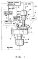
- FIG. 1 shows a polishing apparatus of this embodiment.
- the polishing apparatus has a polishing unit 2 for surface grinding a work piece 1 to become an SOI, and a processing end point detector 3 for detecting an end point of processing the work piece 1 polished by the polishing unit 2.
- FIG. 2 shows a structure of the work piece 1 before processing.
- the work piece 1 has a laminated structure of a first substrate portion 4 and a second substrate portion 5 laminated to the first substrate portion 4, for example, by a pulse electrostatically adhering method.
- the first substrate portion 4 has an Si thin film 6 made of polycrystalline Si, a field oxide film 7 made of SiO2 deposited on the Si thin film 6, a back gate oxide film 8 arranged in an opening 7a of the field oxide film 7, a back gate electrode 9 arranged on the back gate oxide film 8, and a CVD-SiO2 film 10 covering the entire surface of the Si thin film 6 at the side of the back gate electrode 6.
- the back gate oxide film 8 is arranged in parallel with the surface of the substrate portion at a central portion in its depth direction in the opening 7a of the field oxide film 7, and portions of the CVD-SiO2 film 10 and the Si thin film 6 are filled therein at both sides of the back gate oxide film 8.
- the second substrate portion 5 comprises a support substrate 11, and a BPSG film 12 arranged on the support substrate 11.
- the first substrate portion 4 is integrally connected to the second substrate 5 by adhering the BPSG film 12 to the CVD-SiO2 film 10.
- the work piece 1 of this embodiment is surface ground at the Si thin film 6 until the field oxide film 7 is exposed (a region indicated by an imaginary line in FIG. 2).
- the polishing unit 2 for grinding the work piece 1 has a lower surface plate section 13, an upper surface plate section 14 arranged at an upper position oppositely to the lower surface plate 13, and a process control mechanism 21 for electrically controlling the lower surface plate 13 and the upper surface plate 14.
- the polishing unit 2 of this embodiment is supplied with processing solution L from a liquid supply unit 15 to a position to be polished at the work piece 1.
- the lower surface plate section 13 has a lower surface plate 16 formed in a disc, a polishing cloth 17 adhered to the lower surface plate 16 and made, for example, of foamed urethane, and a lower surface plate driving mechanism 18 for holding and rotatably driving the lower surface plate 16.
- the lower surface plate driving mechanism 18 has a holding shaft 18a coaxially coupled to a lower surface of the lower surface plate 16, and a lower surface plate driving motor 18b for supporting and rotatably driving the holding shaft 18a.
- the upper surface plate section 14 has an upper surface plate 19 having a diameter smaller than a radius of the lower surface plate 16, and an upper surface plate driving mechanism 20 for supporting, rotatably driving the upper surface plate 19 and pressurizing the upper surface plate 19 to the lower surface plate 16.
- a polyurethane suction sheet 19a (not shown) for detachably holding the work piece 1 is mounted on a lower surface of the upper surface plate 19.
- the upper surface plate driving mechanism 20 has a holding shaft 20b coaxially coupled to the upper surface plate 19 on a back of the upper surface plate 19, pressurizing means 20c such as, for example, a pneumatic cylinder detachably attached at an upper end of the holding shaft 20b for vertically driving the holding shaft 20b, a solenoid valve 20d for controlling application of pneumatic pressure to the pressurizing means 20c, and an upper surface plate driving motor 20e for holding the upper end of the pressurizing means 20c and rotatably driving it around an axis.
- pressurizing means 20c such as, for example, a pneumatic cylinder detachably attached at an upper end of the holding shaft 20b for vertically driving the holding shaft 20b
- solenoid valve 20d for controlling application of pneumatic pressure to the pressurizing means 20c
- an upper surface plate driving motor 20e for holding the upper end of the pressurizing means 20c and rotatably driving it around an axis.
- the liquid supply unit 15 has a nozzle 22 for injecting processing solution L containing free abrasive to a position to be polished, and a tank 23 for storing the processing solution L to be supplied to the nozzle 22.
- the processing solution L can be suitably selected in response to a material of the layer to be polished.
- the processing solution L contains, for example, colloidal silica and amine. This is mainly because the Si thin film 6 to be polished has small resistance against weak alkaline polishing solution and a hydrate is produced.
- the processing end point detecting unit 3 has a radiation temperature sensor 24 such as, for example, an infrared thermometer arranged oppositely at a predetermined distance to the polishing cloth 17 of the lower surface plate 16 for detecting a surface temperature T of the polishing cloth 17 during polishing, an amplifier 25 for amplifying an electric signal ST indicating the surface temperature T of the polishing cloth 17 output from the radiation temperature sensor 24, and an arithmetic processor 26 inputting the electric signal ST output from the amplifier 25 for calculating the relationship between the surface temperature T of the polishing cloth 17 and the polishing time t based on the electric signal ST.
- a radiation temperature sensor 24 such as, for example, an infrared thermometer arranged oppositely at a predetermined distance to the polishing cloth 17 of the lower surface plate 16 for detecting a surface temperature T of the polishing cloth 17 during polishing
- an amplifier 25 for amplifying an electric signal ST indicating the surface temperature T of the polishing cloth 17 output from the radiation temperature sensor 24, and an arithmetic processor 26 inputting the electric
- the processing control mechanism 21 has a solenoid valve 20d, an upper surface plate driving motor 20e, and a lower surface plate driving motor 18b, and is so provided as to be electrically connected to the liquid supply unit 15 and the arithmetic processor 26 to control polishing process as will be described later.
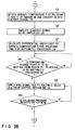
- step S1 the work piece 1 is so vacuum-chucked to the upper surface plate 19 that the Si thin film 6 is opposed to the polishing cloth 17 (step S1). Then, the lower surface plate 16 and the upper surface plate 19 are rotated, the processing solution L is injected to a position to be polished of the work piece 1, and the upper surface plate 19 is moved down. That is, a rotation signal SRD is applied from the process control mechanism 21 to the lower surface driving motor 18b (step S2a), and the lower surface plate 16 is rotated in a direction of an arrow R1, for example at about 60 to 120 rpm (step S3a).
- a rotation signal SRU is applied from the process control mechanism 21 to the upper surface plate driving motor 20e (step S2b), and the upper surface plate 19 is rotated in a direction of an arrow R2, for example, at about 60 to 120 rpm (step S3b). Further, a liquid supply signal SL is applied from the process control mechanism 21 to the liquid supply unit 15 (step S2c), and the processing solution L is injected to the position to be polished of the work piece 1 through the nozzle 22 (step S3c). A down signal SD is applied to the solenoid valve 20d (step S2d), and the upper surface plate 19 is moved down in a direction of an arrow D (step S3d).
- the process control mechanism 21 monitors a pressure of contacting the Si thin film 6 with the polishing cloth 17, i.e., a polishing pressure (step 4), and stops falling of the upper surface plate 19 when the polishing pressure becomes about 200 to 1,600 gf/cm2.
- the Si thin film 6 is surface ground by the free abrasive contained in the processing solution L and the polishing cloth 17.
- the polishing cloth 17 is gradually raised at its surface temperature T by means of frictional heat of the work piece 1 and reaction heat of the Si thin film 5 with amine of the solution L as the polishing is advanced (see FIG. 4).
- the radiation temperature sensor 24 receives an infrared light to be radiated from the polishing cloth 17, detects the surface temperature T of the polishing cloth 17, and converts it into an electric signal ST (step S0).
- This electric signal ST is sent to the amplifier 25, amplified by the amplifier 25 (step S6), and sent to the arithmetic processor 26.
- FIG. 5 schematically shows the relationship between the differential coefficient ⁇ and the polishing time t.
- a region R1 indicates the differential coefficient ⁇ when only the Si thin film 6 is polished.
- the region R1 corresponds to a region R1a in FIG. 4, and it is understood that the surface temperature of the polishing cloth 17 is increased substantially at a constant rate.
- the polishing of the Si thin film 6 is advanced, the field oxide film 7 is exposed and becomes immediately before it is contacted with the polishing cloth 17, the differential coefficient ⁇ becomes a region R2 in FIG. 5. That is, as shown by a region R2a in FIG.
- the increasing rate of the surface temperature T of the polishing cloth 17 is increased as compared with the initial polishing of the Si thin film 6. This is considered that the quantity of generated heat is increased due to an increase in denseness of a portion of an intermediate layer or more as compared with the initial layer of the Si thin film 6.
- the differential coefficient ⁇ becomes a negative value as in a region R3 in FIG. 5. That is, as shown by the region R3a in FIG. 4 corresponding to the region R3, the surface temperature T of the polishing cloth 17 is gradually lowered as the polishing is advanced.
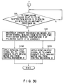
- a temperature change point T1 in FIG. 4 from the region R1 to the region R2 is detected by the arithmetic processor 26 (step S8), the process control mechanism 21 applies a rise signal SD1 to the solenoid valve 20d when the temperature change point T1 is detected (step S9), and a polishing pressure of the upper surface plate 19 to the polishing cloth 17 is reduced, for example, by 10 to 30% (step S10).
- the differential coefficient ⁇ is corrected to the region R1 level. As a result, overheating of the work piece 1 can be prevented.
- the arithmetic processor 26 detects a temperature change point T2 in FIG.
- step S11 applies a rise signal SD2 to the solenoid valve 20d after several minutes from a detecting time point (or after the surface temperature T of the polishing cloth 17 is lowered), thereby operating the pressurizing means 20c reversely (step S12).
- the processing end point detecting unit 3 is provided, and the polishing is controlled based on the detection result of the process end point detecting unit 3. Therefore, a sag (recess) CC (see FIG. 6) of the opening 7a of the field oxide film 7 can be reduced to 1 ⁇ m or less, and the work piece 1 can be efficiently polished. Particularly, since the temperature change point T1 is detected in the step S8 thereby to reduce the polishing pressure of the upper surface plate 19 to the polishing cloth 17, overheat of the work piece 1 can be prevented, thereby further enhancing the sag (recess) suppressing effect.
- the polishing pressure is regulated based on the temperature change point T1 to be shifted from the region R1 to the region R2 as detected.
- the present invention is not limited to the particular embodiment.
- the process is omitted, and an end point of polishing may be merely detected by the temperature change point T2.
- the above-described steps S8 to S10 are omitted.
- the processing end point is detected based on a decrease in the surface temperature of the polishing cloth 17 when the polishing is shifted from the Si thin film 6 to the field oxide film 7.
- the present invention is not limited to the particular embodiment.
- the surface temperature of the polishing cloth might be raised when the polishing is shifted from a certain layer to its adjacent layer.
- the present invention may also be applied to the polishing of such a material.
- a temperature sensor 30 such as, for example, a thermocouple is so buried in the upper surface plate 19 as to be contacted with the rear surface of the adsorption sheet 19a, and a temperature change of the rear surface of the work piece 1 may be directly detected.
- a vacuum chuck having a number of suction holes 32 to be connected to a vacuum source 31 is employed as the upper surface plate 19 and a temperature sensor 30 such as, for example, a thermocouple is buried in a chuck surface in which the suction holes 32 of the vacuum chuck are opened, a temperature change of the rear surface of the work piece 1 can be more accurately detected.
- the present invention is not limited to the steps of grinding and selectively polishing the Si substrate with the field oxide film as a stopper as in the above-described embodiment of the SOI manufacturing process.
- the present invention may also be applied to a detection of an end point of the polishing step for flattening a step due to the back gate electrode 9 by polishing, for example, the CVD-SiO2 film 10.
- FIG. 10 shows the relationship between a polishing time t and a surface temperature T of the polishing cloth 17 when the surface of the CVD-SiO2 film 10 is polished to remove the ruggedness.
- a temperature gradient 82 at the latter period of the polishing becomes remarkably larger than a temperature gradient ⁇ 1 at the initial of the polishing.
- the quantity of generated heat upon polishing is remarkably increased at the latter period of polishing as compared with that at the initial of polishing. This is considered as causes thereof that, since the surface of the CVD-SiO2 film 10 has ruggedness at the initial of polishing (see FIG.
- the contact area of the CVD-SiO2 film 10 with the polishing cloth 17 is small, but when the surface of the CVD-SiO2 film 10 is completely flattened by the polishing, the contact area of the CVD-SiO2 film 10 with the polishing cloth 17 is increased as compared with that at the initial of polishing to increase its frictional resistance thereby to cause the quantity of generated heat to be increased.
- the end point of polishing can be accurately detected, and hence particular effect that the thickness ⁇ d can be severely controlled as the CVD-SiO2 film 10 is flattened is provided.
- the end of polishing may be delayed by a predetermined time ⁇ t from the time point tE. Further, in view of the fact that the increased amount of the differential coefficient ⁇ is increased as compared with that at the initial of polishing when the temperature gradient is not linearly varied at the time point of finishing the polishing to become the thickness ⁇ d, the polishing may be finished at the time point when the differential coefficient ⁇ exceeds a preset threshold value ⁇ T.
- the present invention is not limited to the structure of the work piece 1 of the above-described embodiment in the case of polishing the work piece formed by laminating a plurality of different materials in a laminar state in a cutout direction.
- the present invention may be applied to polishing for flattening a work piece 41 as shown in FIG. 11. That is, this work piece 41 has an Si base substrate 42, a bond substrate (made of Si) 43 fixed to the base substrate 42 and being, for example, 20 ⁇ m thick, and an SiO2 layer 44 inserted between the base substrate 42 and the bond substrate 43 and having a thickness of, for example, 1 ⁇ m.
- an end point in which its thickness ⁇ d1 becomes 2 ⁇ m is detected during polishing of the bond substrate 43 (which is conducted to obtain an active layer for forming a device).
- FIG. 12 shows the relationship between a polishing time t and a surface temperature T of the polishing cloth 17.
- a temperature gradient ⁇ 4 at the latter period of polishing is remarkably increased as compared with a temperature gradient 83 of the initial of polishing.
- the quantity of generated heat is remarkably increased upon polishing at the latter period of polishing as compared with that at the initial of polishing. It is considered as a cause that a heat transfer rate of the SiO2 layer 44 is much lower than that of the bond substrate 43.
- the end of polishing may be delayed by a predetermined time ⁇ t1 to the time point tE1.
- the polishing may be finished at a time point when the differential coefficient ⁇ exceeds a preset threshold value 8T1.
- the method and apparatus for polishing the work piece described above are not limited to the surface grinding as described above, but may be applied to other polishing process such as a curved surface processing, a groove processing.
- polishing exemplifies ordinary polishing.
- present invention may also be applied to mechanical ⁇ chemical polishing (CMP), mechanochemical polishing, etc.
- the polishing is exemplified as the type of polishing.
- the present invention may also be applied to all processing methods in the case of lapping, grinding, surface grinding.
- the present invention may also be applied to one side polishing and both-side polishing.
- FIG. 13 shows a polishing apparatus according to another embodiment of the present invention.
- This polishing apparatus has a polishing unit 51 for surface grinding a thin plate-shaped work piece 1 to become an SOI, and a processing end point detector 52 for detecting an end point of processing the work piece 1 surface ground by the polishing unit 51.
- the work piece 1 to be polished by the polishing apparatus is similar to that shown in FIG. 2, and a detailed description thereof will be omitted.
- the polishing unit 51 has a lower surface plate section 53, an upper surface plate section 54 arranged at an upper position oppositely to the lower surface plate 53, and a process control mechanism 61 for electrically controlling the lower surface plate 53 and the upper surface plate 54.
- the polishing unit 51 of this embodiment is supplied with processing solution L from a liquid supply unit 55 to a position to be polished at the work piece 1.
- the lower surface plate section 53 has a lower surface plate 56 formed in a disc, a polishing cloth 57 adhered to the lower surface plate 56 and made, for example, of foamed urethane, and a lower surface plate driving mechanism 58 for holding and rotatably driving the lower surface plate 56.
- the upper surface plate driving mechanism 60 and the lower surface plate driving mechanism 58 are electrically controlled by the above-described process control mechanism 61.
- the upper surface plate driving mechanism 60 has elevation means 60a such as, for example, a pneumatic cylinder for vertically moving the upper surface plate 59 through a shaft 60b.
- the liquid supply unit 55 has a nozzle 62 for injecting processing solution L containing free abrasive to a position to be polished, and a tank 63 for storing the processing solution L to be supplied to the nozzle 62.
- the processing solution L can be suitably selected in response to a material of the layer to be polished.
- the processing solution L contains, for example, colloidal silica and amine. This is mainly because the Si thin film 6 to be polished has small resistance against weak alkaline polishing solution.
- the processing end point detecting unit 60 has a vibration sensor 64 such as, for example, a semiconductor gage type (or a piezoelectric type or a strain gage type) acceleration pickup, a cantilever with a strain gage attached to a back surface of the upper surface plate 59, an amplifier 65 for amplifying a vibration detection signal SV output from the vibration sensor 65, a band-pass filter 66 for extracting only a frequency component necessary to detect a process end point of the vibration detection signal SV amplified by the amplifier 65, a vibration analyzer 67 inputting the vibration detection signal SF having only a necessary frequency component output from the band-pass filter 66 for analyzing a vibration to be described later, and a process end point detector 68 inputting an analysis signal A in the vibration analyser 67 for detecting a process end point to output a process stop signal SS to the process control mechanism 61.
- a vibration sensor 64 such as, for example, a semiconductor gage type (or a piezoelectric type or a strain gage
- Transmission of a signal from the vibration sensor 64 to the amplifier 65 is so provided as to be conducted by a radio type, and both have antennas for receiving and transmitting the signal. It should be noted that the signal maybe transmitted from the vibration sensor 64 to the amplifier by way of a wired signal line (not shown).
- the band-pass filter 66 is so set as to pass only a vibration detection signal SV of a frequency band of, e.g., 2kHz to 4kHz.
- the vibration analyzer 67 is of an FFT (Fast Fourier Transform) type vibration analyzer to output an analysis signal SA indicating a power spectrum of the frequency band of, e.g., 2kHz - 4kHz.
- the process end point detector 68 is set with a threshold value PT, and so set as to output a process stop signal SS to the process control mechanism 61 if the analysis signal SA output from the vibration analyzer 67 exceeds the threshold value PT.
- the work piece 1 is so adhered to the upper surface plate 59 that the Si thin film 6 is opposed to the polishing cloth 57. Then, a rotation signal SRD is applied from the process control mechanism 61 to the lower surface plate driving mechanism 58, and the lower surface plate 56 is rotated in a direction of an arrow R1, for example at about 60 to 120 rpm.
- a rotation signal SRU and a down signal SD are applied from the process control mechanism 61 to the upper surface plate driving mechanism 60 and the upper surface plate 59 is rotated in a direction of an arrow R2, for example, at about 60 to 120 rpm, and the upper surface plate 59 is moved down in a direction of an arrow R2, and the Si thin film 6 of the work piece 1 is contacted with the polishing cloth 17.
- the upper surface plate 59 is moved down and stopped in the state that the polishing pressure becomes about 200 to 600 gf/cm2.
- the processing solution L is injected to a position to be polished of the work piece 1 through a nozzle 62.
- the Si thin film 6 is surface ground by the free abrasive contained in the processing solution L and the polishing cloth 57.
- a mechanical vibration generated in the case of polishing is detected by the vibration sensor 64, and a vibration detection signal SV is output.
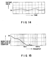
- FIG. 14 shows the vibration detection signal SV at this time.
- the vibration detection signal SV is amplified by the amplifier 65, then a vibration detection signal SF in which only a frequency band of 2kHz to 4kHz is extracted by a band-pass filter 66 is input to the vibration analyzer 67.
- the vibration detection signal SF input to the vibration analyzer 67 is FFT-processed by the vibration analyzer 67, and an analysis signal SA for indicating a power spectrum of the frequency band of, e.g., 2kHz to 4kHz is output to the process end point detector 68.
- FIG. 15 shows the vibration detection signal SA at this time.
- the process stop signal SS is not output to the process control mechanism 61. Therefore, the polishing is continued as it is. Then, the polishing is advanced, and as shown in FIG. 16, the vibration detection signal SV in which the field oxide film 7 is exposed and contacted with the polishing cloth 17 is shown in FIG. 17. That is, as compared with FIG. 14 when only the Si thin film 6 is polished, a level is entirely raised, and its waveform is disordered.
- the analysis signal SA output from the vibration analyzer 67 becomes as shown in FIG. 18. That is, as compared with FIG. 15 when only the Si thin film 6 is polished, it is understood that a level of the frequency band of 2kHz to 4kHz is increased to a level exceeding the threshold value PT.
- the analysis signal SA is input to the process end point detector 68, the analysis signal SA is larger than the threshold value PT, and hence the process stop signal SS is output to the process control mechanism 61.
- rotation stop signals SSU, SSD are applied from the process control mechanism 61 which inputs the process stop signal SS, and a rise signal SU is applied to the upper surface plate driving mechanism 60, thereby stopping polishing.
- a sag a sag (recess) CC (see FIG. 19) of the field oxide film 7 can be reduced to 1 ⁇ m or less.
- the sag (recess) of the opening 7a of the field oxide film 7 can be reduced to 1 ⁇ m or less.
- the one vibration sensor 64 is mounted on the back surface of the upper surface plate 59.
- the present invention is not limited to the particular embodiment.
- a plurality of vibration sensors 64 may be mounted, detections of process end points described above can be processed for the vibration detection signals SF from the respective vibration sensors 64, and their AND or OR operation may be eventually executed.
- the vibration sensor 64 is mounted on the back surface of the upper surface plate 59.
- the vibration sensor 64 may be mounted on a bearing portion of the elevation means 60a, in case that the change in the vibrating pattern or resonance pattern is generated on the bearing portion.
- a vibration sensor 71 (FIG. 13) is mounted on the lower surface of the lower surface plate 56, and the above-described detection of the end point of processing may be conducted based on the vibration detection signal SF1 from the vibration sensor 71. Moreover, a difference between the vibration detection signal SF output from the vibration sensor 64 mounted on the upper surface plate 59 and the vibration detection signal SF1 output from the vibration sensor 71 mounted on the lower surface plate 56 is obtained, and the above-described detection of the end point of processing may be conducted based on a differential signal obtained therefrom.
- the vibration sensor 64 is mounted on the upper surface plate 59, a vibrator 72 is mounted on the lower, a mechanical vibration of a special frequency f of the degree not imparting influence to the processing is generated forcibly by the vibrator 72 during polishing, the vibration at this time is detected by the vibration sensor 64, and the detection of the end point of processing may be conducted based on the vibration detection signal SF extracted only in the frequency band including the above-described special frequency f by a band-pass filter.
- the deciding accuracy of the detection of the end point can be improved.
- the vibration analyser 67 is provided between the band-pass filter 66 and the processing end point detector 68.
- the present invention is not limited to the particular embodiment.
- the vibration analyzer 67 is omitted, and the detection of the end point is executed by a preset threshold value PT to the processing end point detector 68 for the vibration detection signal SF output from the band-pass filter 66.
- the detection of the end point of processing is conducted by comparing the threshold value PT with the analysis signal SA output from the vibration analyzer 67.
- an integrator is provided between the vibration analyzer 67 and the processing end point detector 68, and the detection of the end point of processing may be conducted by the threshold value by the processing end point detector 68 as to the integrated result of the analysis signal SA by the integrator.
- the detection of the end point of processing is executed by utilizing an increase in the amplitude of the frequency component in the power spectrum of the frequency band of, for example, 2 kHz to 4kHz when the field oxide film 7 is exposed and contacted with the polishing cloth 57.
- the detection of the end point of processing may be executed by utilizing the fact that a peak value of the amplitude of the frequency component exists when only the Si thin film 6 is polished in the vicinity of 90 Hz of the power spectrum (this frequency is varied according to the structure of the apparatus) whereas the peak value is vanished (see FIG. 21) when the polishing is advanced, the field oxide film 7 is exposed and contacted with the polishing cloth 57.
- polishing is exemplified.
- any of lapping, grinding, surface grinding may be applied as the processing method.
- both the one side polishing or both side polishing may be applied.
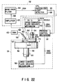
- FIG. 22 shows a polishing apparatus according to still another embodiment of the present invention. Since the polishing apparatus has fundamentally the same structure as that of the polishing apparatus shown in FIG. 13, the same reference symbols as those in FIG. 13 are used to indicate the similar or corresponding structural components, and a description thereof will be omitted. More specifically, this polishing apparatus comprises a polishing unit 51 for surface grinding a thin plate-shaped work piece 1 to become an SOI, and a processing end point detector 52 for detecting an end point of processing the work piece 1 surface ground by the polishing unit 51.
- a polishing unit 51 for surface grinding a thin plate-shaped work piece 1 to become an SOI
- a processing end point detector 52 for detecting an end point of processing the work piece 1 surface ground by the polishing unit 51.
- the polishing unit 51 has a lower surface plate section 53, an upper surface plate section 54 arranged at an upper position oppositely to the lower surface plate 53, and a process control mechanism 61 for electrically controlling the lower surface plate 53 and the upper surface plate 54.
- the polishing unit 51 of this embodiment is supplied with processing solution L from a liquid supply unit 55 to a position to be polished at the work piece 1.
- the upper surface plate section 54 has an upper surface plate 59 having a diameter smaller than a radius of the lower surface plate 56, a wheel-shaped sensor mounting jig 79 (see FIG. 23) fixedly connected to the upper surface of the upper surface plate 59, and an upper surface plate driving mechanism 60 for holding the sensor mounting jig 79 and rotatably driving and applying a polishing pressure thereto.
- the sensor mounting jig 79 has a ring-shaped outer wheel 79a, a circular tube-shaped bearing 79b provided at a concentrical position of the center of the outer wheel 79a, and a rectangular-sectional submembers 79c radially and equidistantly bridged between the outer wheel 79a and the bearing 79b.
- a shaft 60b is engaged with the bearing 79b to be vertically moved up or down by the upper surface plate driving mechanism 60.
- the processing end point detector 52 has an amplifier 65 for amplifying a strain detection signal SM output from a strain gauge 64S attached to the sensor mounting jig 79, and a processing end point detector 68 for comparing to calculate the strain detection signal SM amplified by the amplifier 65 with a preset threshold value ST to output a process stop signal SS to the process control mechanism 61 when the threshold value ST is larger than the strain detection signal SM.
- the strain sensor 64S has a piezoelectric element as its body and mounted partly on the side of the submember 79c to transmit a signal to the amplifier 65 via a radio wave type and with antennas provided for transmitting and receiving the signal.
- the lower surface plate 56 is rotated, for example, in one direction of an arrow R1 at about 60 to 120 rpm
- the upper surface plate 59 is rotated, for example, in a direction of an arrow R2 at about 60 to 120 rpm, moved down in a direction of an arrow D1
- an Si thin film 6 is contacted with a polishing cloth 57.
- a force F of a tangential direction is operated at the sensor mounting jig 79 through the work piece 1 and the upper surface plate 59.
- the submember 79c is deformed due to the force F.
- This strain is converted into a strain detection signal SM having a voltage value of the amplitude responsive to a strain amount by the strain sensor 64S.
- the strain detection signal SM is amplified by the amplifier 65, and compared with a preset threshold value ST by the process end point detector 68.
- a strain ⁇ 1 when only the Si thin film 6 is polished by free abrasive and the polishing cloth 57, a strain ⁇ 1 whereas when the polishing is advanced, the field oxide film 7 is exposed and started to be contacted with the polishing cloth 57, the strain becomes ⁇ 2 due to a reduction in its frictional resistance (which is considered that the field oxide film 7 is harder, scarcely ground and easily slid). That is, when it reaches the process end point, the strain is reduced by ⁇ .
- the threshold value ST is set to between the strains ⁇ 1 and the strain ⁇ 2, thereby detecting the process end point. More particularly, the strain ⁇ 2 at the time of the end point of processing is reduced as compared with the threshold value ST, and a process stop signal SS is output to the process control mechanism 61.
- the polishing apparatus of this embodiment has the process end point detector 52 for detecting the end point of processing in view of the reduction in the strain of the rotating direction upon reduction of the frictional resistance generated at the time of the end point of processing. Therefore, a sag (recess) CC (see. FIG. 19) of the opening 7a of the field oxide film 7 can be set to 1 ⁇ m or less.
- the strain sensor 24S is mounted on the side face of the submember 79c.
- the present invention is not limited to the particular embodiment
- a cutout 79d is provided partly on the outer wheel 79a, and even if the strain sensor 64S is mounted on the cutout 79d, similar effect can be provided. Further, even if a pressure sensor is used instead of the strain sensor, the similar effect can be provided.
Landscapes
- Engineering & Computer Science (AREA)
- Mechanical Engineering (AREA)
- Mechanical Treatment Of Semiconductor (AREA)
- Finish Polishing, Edge Sharpening, And Grinding By Specific Grinding Devices (AREA)
Applications Claiming Priority (6)
| Application Number | Priority Date | Filing Date | Title |
|---|---|---|---|
| JP5347893 | 1993-03-15 | ||
| JP53478/93 | 1993-03-15 | ||
| JP9032793A JPH06320416A (ja) | 1993-03-15 | 1993-04-19 | 研磨方法及び研磨装置 |
| JP90327/93 | 1993-04-19 | ||
| JP5235286A JPH0794452A (ja) | 1993-09-22 | 1993-09-22 | 研磨方法及び研磨装置 |
| JP235286/93 | 1993-09-22 |
Publications (2)
| Publication Number | Publication Date |
|---|---|
| EP0616362A2 true EP0616362A2 (de) | 1994-09-21 |
| EP0616362A3 EP0616362A3 (de) | 1995-06-21 |
Family
ID=27294962
Family Applications (1)
| Application Number | Title | Priority Date | Filing Date |
|---|---|---|---|
| EP94103889A Ceased EP0616362A3 (de) | 1993-03-15 | 1994-03-14 | Verfahren zum Polieren von Werkstücken und Vorrichtung dafür. |
Country Status (2)
| Country | Link |
|---|---|
| EP (1) | EP0616362A3 (de) |
| KR (1) | KR940022734A (de) |
Cited By (15)
| Publication number | Priority date | Publication date | Assignee | Title |
|---|---|---|---|---|
| EP0771611A1 (de) * | 1995-11-02 | 1997-05-07 | Ebara Corporation | Verfahren und Gerät zur Ermittlung des Endes eines Polierverfahrens |
| US5851846A (en) * | 1994-12-22 | 1998-12-22 | Nippondenso Co., Ltd. | Polishing method for SOI |
| EP0810064A3 (de) * | 1996-05-30 | 1998-12-23 | Ebara Corporation | Poliervorrichtung mit Verriegelungsfunktion |
| WO2000054934A1 (en) * | 1999-03-17 | 2000-09-21 | Advanced Micro Devices, Inc. | The endpoint of a chemical-mechanical polishing operation |
| DE19949976C1 (de) * | 1999-10-08 | 2000-11-16 | Univ Dresden Tech | Verfahren und Anordnung zur in-situ Endpunkterkennung beim chemisch-mechanischen Polieren (CMP) von Schichten auf Halbleiterwafern |
| WO2000077847A1 (fr) * | 1999-06-15 | 2000-12-21 | Commissariat A L'energie Atomique | Procede de realisation d'interconnexions notamment en cuivre pour dispositifs micro-electroniques |
| US6375540B1 (en) * | 2000-06-30 | 2002-04-23 | Lam Research Corporation | End-point detection system for chemical mechanical posing applications |
| DE19726665C2 (de) * | 1997-06-23 | 2002-06-27 | Univ Dresden Tech | Verfahren und Anordnung zur in-situ-Endpunktermittlung beim CMP |
| WO2003002301A1 (en) * | 2001-06-26 | 2003-01-09 | Lam Research Corporation | End point detection system for chemical mechanical polishing applications |
| DE102008045216A1 (de) | 2007-08-23 | 2009-04-09 | Technische Universität Dresden | Verfahren und Anordnung zum Erkennen des Endpunktes beim Polieren von eingebetteten SiN-Strukturen auf Halbleiterwafern |
| US8092707B2 (en) | 1997-04-30 | 2012-01-10 | 3M Innovative Properties Company | Compositions and methods for modifying a surface suited for semiconductor fabrication |
| CN111037444A (zh) * | 2019-12-23 | 2020-04-21 | 北京迪蒙吉意超硬材料技术有限公司 | 一种温度和压力自适应的聚晶金刚石复合片表面抛光机 |
| CN111316403A (zh) * | 2018-03-12 | 2020-06-19 | 应用材料公司 | 在抛光原位监测期间的滤波 |
| US20220266418A1 (en) * | 2021-02-22 | 2022-08-25 | Ebara Corporation | Substrate processing apparatus |
| US12569956B2 (en) | 2021-02-22 | 2026-03-10 | Kioxia Corporation | Control method for processing of a substrate |
Families Citing this family (1)
| Publication number | Priority date | Publication date | Assignee | Title |
|---|---|---|---|---|
| KR100673185B1 (ko) * | 2000-04-11 | 2007-01-22 | 주식회사 하이닉스반도체 | 화학적 기계적 연마 방법 |
Family Cites Families (3)
| Publication number | Priority date | Publication date | Assignee | Title |
|---|---|---|---|---|
| US4358338A (en) * | 1980-05-16 | 1982-11-09 | Varian Associates, Inc. | End point detection method for physical etching process |
| JPH02137852A (ja) * | 1988-11-18 | 1990-05-28 | Dainippon Screen Mfg Co Ltd | フォトレジストの現像終点検出方法 |
| US5196353A (en) * | 1992-01-03 | 1993-03-23 | Micron Technology, Inc. | Method for controlling a semiconductor (CMP) process by measuring a surface temperature and developing a thermal image of the wafer |
-
1994
- 1994-03-14 EP EP94103889A patent/EP0616362A3/de not_active Ceased
- 1994-03-14 KR KR1019940004968A patent/KR940022734A/ko not_active Ceased
Cited By (23)
| Publication number | Priority date | Publication date | Assignee | Title |
|---|---|---|---|---|
| US5851846A (en) * | 1994-12-22 | 1998-12-22 | Nippondenso Co., Ltd. | Polishing method for SOI |
| EP0771611A1 (de) * | 1995-11-02 | 1997-05-07 | Ebara Corporation | Verfahren und Gerät zur Ermittlung des Endes eines Polierverfahrens |
| US5830041A (en) * | 1995-11-02 | 1998-11-03 | Ebara Corporation | Method and apparatus for determining endpoint during a polishing process |
| EP0810064A3 (de) * | 1996-05-30 | 1998-12-23 | Ebara Corporation | Poliervorrichtung mit Verriegelungsfunktion |
| US5904608A (en) * | 1996-05-30 | 1999-05-18 | Ebara Corporation | Polishing apparatus having interlock function |
| EP1704962A3 (de) * | 1996-05-30 | 2007-08-01 | Ebara Corporation | Poliervorrichtung mit Verriegelungsfunktion |
| EP1213094A3 (de) * | 1996-05-30 | 2003-01-08 | Ebara Corporation | Poliervorrichtung mit Verriegelungsfunktion |
| US8092707B2 (en) | 1997-04-30 | 2012-01-10 | 3M Innovative Properties Company | Compositions and methods for modifying a surface suited for semiconductor fabrication |
| DE19726665C2 (de) * | 1997-06-23 | 2002-06-27 | Univ Dresden Tech | Verfahren und Anordnung zur in-situ-Endpunktermittlung beim CMP |
| WO2000054934A1 (en) * | 1999-03-17 | 2000-09-21 | Advanced Micro Devices, Inc. | The endpoint of a chemical-mechanical polishing operation |
| US6179688B1 (en) | 1999-03-17 | 2001-01-30 | Advanced Micro Devices, Inc. | Method and apparatus for detecting the endpoint of a chemical-mechanical polishing operation |
| US6572443B1 (en) | 1999-03-17 | 2003-06-03 | Advanced Micro Devices Inc. | Method and apparatus for detecting a process endpoint |
| WO2000077847A1 (fr) * | 1999-06-15 | 2000-12-21 | Commissariat A L'energie Atomique | Procede de realisation d'interconnexions notamment en cuivre pour dispositifs micro-electroniques |
| DE19949976C1 (de) * | 1999-10-08 | 2000-11-16 | Univ Dresden Tech | Verfahren und Anordnung zur in-situ Endpunkterkennung beim chemisch-mechanischen Polieren (CMP) von Schichten auf Halbleiterwafern |
| US6375540B1 (en) * | 2000-06-30 | 2002-04-23 | Lam Research Corporation | End-point detection system for chemical mechanical posing applications |
| US6726530B2 (en) | 2000-06-30 | 2004-04-27 | Lam Research Corporation | End-point detection system for chemical mechanical polishing applications |
| WO2003002301A1 (en) * | 2001-06-26 | 2003-01-09 | Lam Research Corporation | End point detection system for chemical mechanical polishing applications |
| DE102008045216A1 (de) | 2007-08-23 | 2009-04-09 | Technische Universität Dresden | Verfahren und Anordnung zum Erkennen des Endpunktes beim Polieren von eingebetteten SiN-Strukturen auf Halbleiterwafern |
| CN111316403A (zh) * | 2018-03-12 | 2020-06-19 | 应用材料公司 | 在抛光原位监测期间的滤波 |
| CN111316403B (zh) * | 2018-03-12 | 2024-12-13 | 应用材料公司 | 在抛光原位监测期间的滤波 |
| CN111037444A (zh) * | 2019-12-23 | 2020-04-21 | 北京迪蒙吉意超硬材料技术有限公司 | 一种温度和压力自适应的聚晶金刚石复合片表面抛光机 |
| US20220266418A1 (en) * | 2021-02-22 | 2022-08-25 | Ebara Corporation | Substrate processing apparatus |
| US12569956B2 (en) | 2021-02-22 | 2026-03-10 | Kioxia Corporation | Control method for processing of a substrate |
Also Published As
| Publication number | Publication date |
|---|---|
| EP0616362A3 (de) | 1995-06-21 |
| KR940022734A (ko) | 1994-10-21 |
Similar Documents
| Publication | Publication Date | Title |
|---|---|---|
| US6925348B2 (en) | Methods for detecting transitions of wafer surface properties in chemical mechanical polishing for process status and control | |
| US6120347A (en) | System for real-time control of semiconductor wafer polishing | |
| US5842909A (en) | System for real-time control of semiconductor wafer polishing including heater | |
| US6872122B2 (en) | Apparatus and method of detecting a substrate in a carrier head | |
| US5643060A (en) | System for real-time control of semiconductor wafer polishing including heater | |
| US5036015A (en) | Method of endpoint detection during chemical/mechanical planarization of semiconductor wafers | |
| US5240552A (en) | Chemical mechanical planarization (CMP) of a semiconductor wafer using acoustical waves for in-situ end point detection | |
| US5667424A (en) | New chemical mechanical planarization (CMP) end point detection apparatus | |
| US5069002A (en) | Apparatus for endpoint detection during mechanical planarization of semiconductor wafers | |
| US6910942B1 (en) | Semiconductor wafer chemical-mechanical planarization process monitoring and end-point detection method and apparatus | |
| JP3292243B2 (ja) | 研磨終点検出装置 | |
| WO2005043132A1 (en) | Polishing endpoint detection system and method using friction sensor | |
| JP7745073B2 (ja) | 化学機械研磨中の音響信号による平坦化の検出 | |
| US20230009048A1 (en) | Coupling of acoustic sensor for chemical mechanical polishing | |
| JPH06320416A (ja) | 研磨方法及び研磨装置 | |
| US7059939B2 (en) | Polishing pad conditioner and monitoring method therefor | |
| JPH0724708A (ja) | 研磨方法及び研磨装置 | |
| JP4326985B2 (ja) | ウエーハ研磨方法 | |
| JPH10180625A (ja) | 研磨方法および研磨装置 | |
| JPH08243917A (ja) | 研磨の終点検出方法及び研磨装置並びにそれを用いた半導体装置製造方法 | |
| JP2005268330A (ja) | 半導体ウェーハの研磨方法 | |
| KR20020030589A (ko) | 화학 기계적 연마장치 |
Legal Events
| Date | Code | Title | Description |
|---|---|---|---|
| PUAI | Public reference made under article 153(3) epc to a published international application that has entered the european phase |
Free format text: ORIGINAL CODE: 0009012 |
|
| 17P | Request for examination filed |
Effective date: 19940318 |
|
| AK | Designated contracting states |
Kind code of ref document: A2 Designated state(s): DE FR GB NL |
|
| RHK1 | Main classification (correction) |
Ipc: B24B 49/00 |
|
| PUAL | Search report despatched |
Free format text: ORIGINAL CODE: 0009013 |
|
| AK | Designated contracting states |
Kind code of ref document: A3 Designated state(s): DE FR GB NL |
|
| 17Q | First examination report despatched |
Effective date: 19970418 |
|
| GRAG | Despatch of communication of intention to grant |
Free format text: ORIGINAL CODE: EPIDOS AGRA |
|
| STAA | Information on the status of an ep patent application or granted ep patent |
Free format text: STATUS: THE APPLICATION HAS BEEN REFUSED |
|
| 18R | Application refused |
Effective date: 19980927 |