EP0616464B1 - Processeur de signal - Google Patents
Processeur de signal Download PDFInfo
- Publication number
- EP0616464B1 EP0616464B1 EP94301799A EP94301799A EP0616464B1 EP 0616464 B1 EP0616464 B1 EP 0616464B1 EP 94301799 A EP94301799 A EP 94301799A EP 94301799 A EP94301799 A EP 94301799A EP 0616464 B1 EP0616464 B1 EP 0616464B1
- Authority
- EP
- European Patent Office
- Prior art keywords
- signal
- signals
- processor according
- signal processor
- present
- Prior art date
- Legal status (The legal status is an assumption and is not a legal conclusion. Google has not performed a legal analysis and makes no representation as to the accuracy of the status listed.)
- Expired - Lifetime
Links
- 238000006243 chemical reaction Methods 0.000 claims description 8
- 238000010586 diagram Methods 0.000 description 27
- 238000000034 method Methods 0.000 description 19
- 238000012545 processing Methods 0.000 description 19
- 230000008569 process Effects 0.000 description 15
- 238000012546 transfer Methods 0.000 description 11
- 230000014509 gene expression Effects 0.000 description 7
- 230000004044 response Effects 0.000 description 7
- 238000009825 accumulation Methods 0.000 description 4
- 239000003990 capacitor Substances 0.000 description 3
- 230000015654 memory Effects 0.000 description 3
- 230000002829 reductive effect Effects 0.000 description 2
- 239000004065 semiconductor Substances 0.000 description 2
- 239000000758 substrate Substances 0.000 description 2
- 238000012935 Averaging Methods 0.000 description 1
- 230000003321 amplification Effects 0.000 description 1
- 230000015556 catabolic process Effects 0.000 description 1
- 230000008878 coupling Effects 0.000 description 1
- 238000010168 coupling process Methods 0.000 description 1
- 238000005859 coupling reaction Methods 0.000 description 1
- 230000003247 decreasing effect Effects 0.000 description 1
- 238000006731 degradation reaction Methods 0.000 description 1
- 230000001066 destructive effect Effects 0.000 description 1
- 230000000694 effects Effects 0.000 description 1
- 230000005669 field effect Effects 0.000 description 1
- 230000006698 induction Effects 0.000 description 1
- 230000010365 information processing Effects 0.000 description 1
- 230000000670 limiting effect Effects 0.000 description 1
- 239000000463 material Substances 0.000 description 1
- 230000004048 modification Effects 0.000 description 1
- 238000012986 modification Methods 0.000 description 1
- 238000003199 nucleic acid amplification method Methods 0.000 description 1
- 230000003071 parasitic effect Effects 0.000 description 1
- 230000036961 partial effect Effects 0.000 description 1
- 230000002093 peripheral effect Effects 0.000 description 1
- 238000005215 recombination Methods 0.000 description 1
- 230000006798 recombination Effects 0.000 description 1
- 230000009467 reduction Effects 0.000 description 1
- 230000003068 static effect Effects 0.000 description 1
- 238000006467 substitution reaction Methods 0.000 description 1
- 230000001131 transforming effect Effects 0.000 description 1
Images


Classifications
-
- H—ELECTRICITY
- H04—ELECTRIC COMMUNICATION TECHNIQUE
- H04N—PICTORIAL COMMUNICATION, e.g. TELEVISION
- H04N25/00—Circuitry of solid-state image sensors [SSIS]; Control thereof
- H04N25/70—SSIS architectures; Circuits associated therewith
- H04N25/76—Addressed sensors, e.g. MOS or CMOS sensors
-
- H—ELECTRICITY
- H04—ELECTRIC COMMUNICATION TECHNIQUE
- H04N—PICTORIAL COMMUNICATION, e.g. TELEVISION
- H04N25/00—Circuitry of solid-state image sensors [SSIS]; Control thereof
- H04N25/40—Extracting pixel data from image sensors by controlling scanning circuits, e.g. by modifying the number of pixels sampled or to be sampled
- H04N25/46—Extracting pixel data from image sensors by controlling scanning circuits, e.g. by modifying the number of pixels sampled or to be sampled by combining or binning pixels
-
- H—ELECTRICITY
- H04—ELECTRIC COMMUNICATION TECHNIQUE
- H04N—PICTORIAL COMMUNICATION, e.g. TELEVISION
- H04N25/00—Circuitry of solid-state image sensors [SSIS]; Control thereof
- H04N25/70—SSIS architectures; Circuits associated therewith
- H04N25/76—Addressed sensors, e.g. MOS or CMOS sensors
- H04N25/779—Circuitry for scanning or addressing the pixel array
-
- H—ELECTRICITY
- H04—ELECTRIC COMMUNICATION TECHNIQUE
- H04N—PICTORIAL COMMUNICATION, e.g. TELEVISION
- H04N25/00—Circuitry of solid-state image sensors [SSIS]; Control thereof
- H04N25/70—SSIS architectures; Circuits associated therewith
- H04N25/76—Addressed sensors, e.g. MOS or CMOS sensors
- H04N25/7795—Circuitry for generating timing or clock signals
Definitions
- the present invention relates to a signal processor for processing plural signals and used for information storage devices, photoelectric converters, and the like.
- ROMs read-only memories
- a X-Y address system configuration is employed, where a shift register performs a vertical scanning operation and a horizontal scanning operation to output sequentially chronologically externally output signals from signal sources such as memory cells and photo cells.
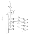
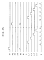
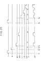
- Fig. 1 is a circuit diagram showing the conventional signal processor.
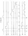
- Fig. 2 is a drive timing chart for the conventional signal processor.
- signal sources S1, S2, S3, and S4 are typical photo cells each for outputting a voltage.
- the photo signals are chronologically outputted to the output line 5 via N-type MOS transistors M11, M12, ... M14, M21, M22 ... M24 acting as switching elements, and capacitance elements C11, C12 ... C14 acting as signal holding means.
- the signal sources are over 100 in number, and is recently over 100 thousands in number.
- the signals from the signal sources are output as visible images. In such images the case may occur where a bright signal occupies only a very small region in one frame and a dark signal occupies the remaining region thereof as if a match flames in the dark.
- the conventional signal processor performs necessary image signal process by outputting all cell signals chronologically and then storing them in an external random access memory.
- the conventional processor is adequate for general purpose devices.
- the processing rate cannot be improved because access to all cells causes unnecessary signal output time when the process to be performed uses only a partial signal.
- a concern of the present invention is to provide a signal processor which can provide an improved processing speed.
- Another concern of the present invention is to provide a small signal processor which can perform a signal process with its relatively simplified circuit configuration and at an inexpensive cost.
- a further concern of the present invention is to provide a signal processor which can be integrated in a signal semiconductor chip which outputs a mixed signal and a discrete signal.
- U.S. Patent Specification No. US-A-4996413 discloses an image detector having an array of photodetectors arranged in rows and columns, and a plurality of holding means for holding outputs from the photodetectors. Output signals from the holding means are mixed to reduce the likelihood of signal degradation.
- German Patent Specification No DE-C-4123203 discloses a sensor capable of outputting within an image a high level part and a low level part. This arrangement allows an increase in processing speed and a reduction of processing costs.
- mixed signals less in number than the number of signal sources is obtained by mixing suitable discrete signals from the signal sources.
- the signal processing rate can be largely improved because of a small number of discrete signals to be processed.
- the small number of discrete signals can reduce the scale of the peripheral circuits, thus widening the applicability to systems.
- the mixed signals which are representative of plural original discrete signals and include nondestructive information, are particularly effective when information is processed at low resolution.
- 200 signal sources are divided to 10 blocks, one block including 20 signal sources.
- the signal mixing means is arranged to each block and mixes 20 discrete signals in each block to make 10 mixed signals in total.
- the signal processing system in the rear stage becomes reduced in scale such that only 10 discrete events, or 1/20 of 200 discrete events, are treated.
- the common image reading operation is established by specifying plural adjacent photo cells as signal sources to be mixed although the resolution may be degraded, compared with with no mixing case.
- the present invention is preferably employed in the case where an entire image trend is desired to read at high speed rather than high resolution.
- the signal mixing means can read a discrete signal from each cell within a necessary block by controllably stopping the operation of the signal mixing means after the mixed signal reading operation.
- passive elements such as capacitors and resistors and active elements such as diodes and transistors are used for the signal source.
- a photo cell such as a photoelectric element and a photoconductive element is particularly preferable as the signal source to produce an electrical signal including information.
- a nondestructive readout-type photo cell which uses a field effect transistor and a static induction transistor with a charge accumulating gate and a bipolar transistor with a charge accumulating base (to be described), is more preferably used for the photo cell.
- a capacitance element as well as a latch circuit are used as signal holding means according to the embodiment of the present invention.
- a sample and hold circuit including a capacitance element is used in concrete when an analog signal is treated.
- the signal mixing means it is preferable to use a transistor and a charge coupled element as a switching element connecting plural capacitance elements. Adding means is used as the mixing means in the present embodiment.
- photo cells S1, S2, S3, and S4 are arranged one-dimensionally as signal sources to output an average signal in two pixel units.
- the configuration is different from the conventional configuration in that a scanning circuit 11', MOS FETs M31, M32, M33, and M34 acting as switching elements, an output line 5', a capacitance element c2', and the like are arranged as the signal mixing means in addition to the structure shown in Figure 1.
- signals are chronologically processed in group (block) units including two cells.
- a reset MOS FET MR' is connected to the output line 5'.
- the reset MOS FET resets the potential of the capacitance element C2' associated with the output line 5' to the reference potential of the terminal 3' when a clock pulse is applied to the terminal 2'.
- Numeral 10' represents an amplifier similar to the amplifier 10.
- Numeral 12' represents an output terminal similar to the output terminal 12.
- a signal reading pulse is applied to the terminal 1 at the time t 1 .
- the photo signals from the cells S1, S2, S3, and S4 are simultaneously read to the capacitance elements C11, C12, C13, and C14.
- the scanning circuit 11' When the scanning circuit 11' outputs the scanning pulse to the output line N1 at the time t 2 , the two MOS transistors M31 and M32 are simultaneously turned on. Then the average signal of photo signals accumulated to the cells S1 and S2 is outputted to the terminal 12' via the capacitance element C2' and the amplifier 10'. Then when a reset pulse is applied to the terminal 2' at the time t 3 , the transistor MR' is turned on while the output line 5' is reset. The block signal reading is completed by executing the above scanning operation to all clocks.
- the scanning circuit 11' can start driving from an arbitrary cell and end driving to an arbitrary cell, only a signal for a necessary block can be read out.
- photo signals can be read at the substantially same time as that for image information obtained through the block reading operation.
- a bipolar transistor with an emitter connected to a capacitance load and a base accumulating optically produced charges is desirable as the nondestructive read-out type sensor.
- the above bipolar transistor is disclosed, for example, in USP 4,791,469 which is entitled “Photoelectric Converter”, invented by Tadahiro OHMI and Nobuyoshi TANAKA, and USP 4,810,896 which is entitled “Photoelectric Conversion Device with Reduced Fixed Pattern Noises", invented by Nobuyoshi TANAKA.
- Fig. 5 is a circuit diagram showing the signal processor according to another embodiment of the present invention.
- the signal processor is different from the first embodiment in that the output signal from a single source is held by two capacitance elements via an amplifier and two switches.
- the first embodiment twice requires a signal holding operation to the capacitance element, the second embodiment can complete the signal holding operation once.
- the amplifiers A1 to A4 amplify signals for all cells S1 to S4 so that the amplified signals are simultaneously held to the capacitance elements C11 to C14 and C11' to C14'.
- the amplifier 10' amplifies again the average signal held in the two capacitance elements C11' and C12' on the capacitance C2' to output to the terminal 12'. Then after the reset MOS FET MR' has reset the potential of the output line 5', the average of the output signals held in the two capacitance elements C13' and C14' is outputted in response to the shift pulse N 2 . This process is sequentially performed to output chronologically the average value for each block to the terminal 12'.
- the scanning circuit 11 operates to output sequentially the signal from each cell.
- the shift pulses are sequentially supplied to the output lines L1 to L4 so that the output signals for respective cells held in the capacitance elements C11 to C14 are sequentially chronologically outputted to the terminal 12.
- a nondestructive readout-type can be used as a signal source.
- the amplifiers A1 to A4 also are not essential as if the signal source has a sufficient low output impedance, they can be omitted.
- Fig. 6 is a circuit diagram for the signal processor according to a third embodiment of the present invention.
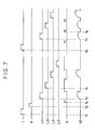
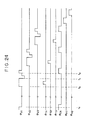
- Fig. 7 is a drive timing chart for the signal processor according to the third embodiment of the present invention.
- switching elements are arranged to connect in common capacitance elements in a group to one another.
- V1, V2, V3, and V4 are signal voltages read to two capacitance elements C11 and C12, C13, and C14, respectively
- Vc12, Vc12, ... are respectively the voltages after two capacitance elements are connected.
- the scanning time for outputting the average value is much shorter than the sum of the cell scanning time.
- the signals for the cells S1 to S4 are held again by the capacitance elements C11 to C14 at the time t 6 .
- the MOS FETs M21 to M24 are sequentially turned on so that the signals held by the respective capacitance elements C11 to C14 appear sequentially chronologically on the terminal 12.
- the third embodiment employs a structure such that an amplifier is arranged to the output of the signal source and/or plural holding means are arranged a single signal source.
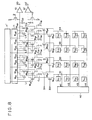
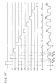
- Fig. 8 shows a circuit diagram for the signal processor according to a fourth embodiment of the present invention.
- an arrangement similar to the first embodiment is applied to the two-dimensional sensor to output the average signal of the plural pixels (cells, for example, two pixels in the present embodiment) in vertical direction.
- a pulse is applied from the vertical scanning circuit 40 to the drive selection line H1 at the time t 1 .
- Photo signals from the cells S11, S12, S13, and S14 for one column line are read out to the vertical lines 51, 52, 53, and 54 at the time t 1 , respectively.
- the MOS transistors M11, M12, M13, and M14 are turned on, whereby the photo signals are held to the capacitance elements C11, C13, C15, and C17.
- the horizontal scanning circuit 11' outputs sequentially pulses to the output lines L1, L2, L3, and L4 so that the average signal of a pair of photo signals stored in the capacitance elements C11, C12, C13, C14, C15, C16, C17 and C18 is outputted to the terminal 20.
- the following two drive selection lines H3 and H4 are selected to output sequentially chronologically the average signal of the adjacent cells arranged in the direction of two column lines.
- Fig. 10 is a circuit diagram for the signal processor according to a fifth embodiment of the present invention.
- the signal processor according to the fifth embodiment is similar to the third embodiment but applied to a two-dimensional sensor.
- a pulse is applied to the terminal 4 to connect two capacitance elements.
- an average signal is obtained and then sequentially scanned.
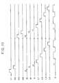
- Fig. 11 is a drive timing chart for the fifth embodiment.
- the MOS transistors M11 to M14 are turned on, thus holding the signals in the capacitance elements C11, C13, C15, and C17.
- the MOS transistors M21 to M24 are turned on, thus holding the signals in the capacitance elements C12, C14, C16, and C18.
- a pulse is applied to the terminal 4 and the MOS transistors M31 to M34 are turned on to connect a pair of capacitance elements, respectively.
- the average value of the output lines for two cells can be obtained every two vertical lines.
- the average value outputting as well as the reset operation are repeated by combining an application of the reset pulse to the terminal 2 and an application of the pulses to the output lines L1 to L4.
- the drive selection lines H1 to H4 are selected sequentially and one by one to hold signals in the capacitance elements C11, C13, C15, and C17. Since the scanning is sequentially made in accordance with the pulses L1 and L3, the output signal amplified for each cell appears as a time series signal to the terminal 12.
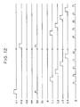
- Fig 13 is a circuit diagram for the signal processor according to the sixth embodiment of the present invention.
- the average value of them is obtained by mixing them.
- Figs. 14 and 15 are drive timing charts for the present embodiment.
- the signals from four adjacent cells are held and then mixed.
- the average value amplified is outputted to the terminal 12 in response to the pulse L1.
- a reset operation is performed during the period T RS .
- Sequentially the signals held in the next four adjacent cells are mixed and then outputted. Then the reset operation is resumed.
- the signal for each cell is sequentially outputted to the terminal 12, as shown in Fig. 15.
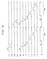
- Fig. 16 shows a seventh embodiment according to the present invention.
- the signal sources S1, S2, S3, and S4 are arranged one-directionally to output the signal from each signal source as well as the average signal of the adjacent signals.
- the signal Si is first outputted, the signals Si and S i+1 are then outputted, and the signal S i+1 is sequentially outputted. Since the average signal from the adjacent signal sources is serially outputted between the signals from the original signal sources, the image resolution can be artificially improved.
- the signal source is one-dimensionally arranged in the present embodiment.
- the image resolution can be two-dimensionally improved by two-dimensionally arranging the signal source to perform the same operation to the vertical signal.
- the signal from the photo cell is outputted as an outline underlining signal.
- ⁇ 2 f ( ⁇ 2 f/ ⁇ x 2 ) + ( ⁇ 2 f/ ⁇ y 2 )
- the transforming method is effective to the one-dimensional image data. That is, subtracting the Laplacian (the average value of the horizontally and vertically adjacent images) of the image from the original image can weaken the image blur, thus realizing the underlined image.
- the operation is substantially the same as that of the conventional signal processor.
- the scanning circuit 12 transfers the signal held in the capacitance Cij to the output line 5.
- the MOS transistors T13, T22, and T31 are turned on.
- the charges stored in the capacitance C22 are transferred to the output line 5 while the charges stored in the capacitances C13 and C31 are transferred to the output line 5'.
- a dummy MOS transistor is connected to the output line 5 to equalize the wiring structure so that the capacitances C3 and C3' are agreed to each other. Moreover setting the dummy capacitance C D to value C can equalize the denominators of the expressions (6.5) and (6.6) to each other. Hence the element 30 can produce the difference (V5 - V5').
- the photoelectric conversion device can calculate the expression (6.3) to underline the image.
- the one-dimensional photoelectric conversion device is shown to simplify the explanation thereof. It is apparent that a two-dimensional photoelectric conversion device can underline the image by operating the expression (6.2) on the same chip in the same manner.
- the expression (6.3) is operated in order to underline the outline of an image.
- the holding capacitance values are set in accordance with the expressions (6.4) and (6.8). If necessary, the values may be readily varied.
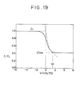
- a MOS capacitance forming the capacitance element indicates the capacitance characteristics with respect to the gate to substrate voltage, as shown in Fig. 19. Therefore in the present invention, the holding means formed of a MOS capacitance can be externally adjusted in its capacitance value by varying the substrate potential.
- Fig. 20 is a circuit diagram for the signal processor according to the ninth embodiment of the present invention and Fig. 21 is its drive timing chart.
- the present embodiment differs from the third embodiment shown in Fig. 6 in that the scanning circuit 11' and the MOS transistors M51 and M52 are prepared to output sequentially the average value.
- a pulse at a high level is inputted to the terminal 1 at the time t 1 to hold the output signals of all the cells S1 to S4 to the capacitance elements C11 to C14, respectively.
- a pulse at a high level is inputted to the terminal 4 at the time t 2 so that two adjacent capacitance elements are connected in common to mix signals.
- the common output line 5 is once reset to the reset potential of the terminal 3.
- the scanning circuit 11' inputs a pulse at a high level to the gate of the MOS transistor M51 at the time t 4 to output the average value.
- the pulse at high level of the sequential scanning circuit 11' is shifted and then the average value amplified chronologically is outputted to the terminal 12.
- the discrete signal outputting operation is performed for each cell. Signals of all the cells S1 to S4 are held to the capacitance elements C11 to C14 at the time t 5 . Next the scanning circuit 11 supplies a shift pulse at a high level to the gate of the MOS transistor M21 at the time t 6 to output the signal of the cell S1 to the terminal 12. Since the pulse at a high level is shifted to the output lines L1 to L4, the signals of all the cells are amplified as sequential time series signals that appear on the terminal 12.
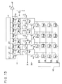
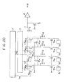
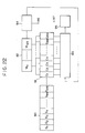
- Fig. 22 is a block diagram showing a system employing the signal processor according to the present invention.
- the sample hold circuit 91 acting as signal holding means holds respectively 200 output signals in total as signals for 200 cells from the cell array 90 acting as a signal source.
- the signal mixing means 92 mixes four adjacent signals using the signals held to produce discrete 50 mixed signals.
- the mixed signal processing circuit 94 processes the compressed signals, determines the area to be subjected to a high resolution signal process, and then supplies the area specifying signal to the discrete signal processing circuit 93. If the discrete signal processing circuit specifies the first block in the cells S1 to S4 as a specified area, only the discrete signal is taken out of the sample and hold circuit 91 corresponding to the first block to execute a signal process.
- the output terminal 96 produces low resolution (low density) information based on the compressed mixed signal, the information of the entire signals can be roughly obtained.
- high resolution (high density) information of a specific area is provided at the output terminal, detailed information of a part of the entire signal can be obtained.
- the signal processing rate can be improved.
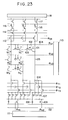
- Fig. 23 is a drawing indicating best the feature of the tenth embodiment of the present invention.
- numeral 101 represents a sensor bipolar transistor
- 102 represents a drive MOS capacitance
- 103 represents a base reset MOS transistor
- 104 represents a drive wiring
- 105 represents an output wiring
- 106 represents a signal transfer MOS transistor
- 107 represents an input transistor for a MOS-type inversion amplifier
- 108 represents a load resistor for the MOS-type inversion amplifier
- 109 represents a horizontal transfer MOS transistor
- 110 represents a vertical shift register for supplying a drive signal to the drive wiring
- 111 represents a horizontal shift register for driving the horizontal transfer MOS transistor
- 112 represents a common output line
- 113 represents an emitter reset MOS transistor.
- Numeral 114 represents a signal transfer MOS transistor
- 115 represents an input transistor for a second MOS-type inversion amplifier
- 116 represents a load resistor for the second MOS-type inversion amplifier
- 117 represents a second horizontal transfer transistor
- 119 represents a second horizontal shift transistor
- 119 represents a second common line.
- the operation of the present embodiment includes (1) accumulating operation (2) reading operation, and (3) resetting operation.
- the accumulating operation starts from the time (time t a ) when a bias is reversely applied between the base and emitter of the sensor bipolar transistor 101 after a completion of the reset operation.
- the base potential increases as holes produced due to incident light are accumulated in the base region and the depletion layer between the base and the collector.
- the reading operation starts when the base potential is positively boosted via the capacitive coupling of the drive MOS capacitance 106 to bias forward between the base and the emitter.
- the transfer MOS transistor Since the emitter potential comes to a certain potential difference near to the base potential due to the capacitance load, the differential of the base potential at the accumulating operation appears on the emitter terminal. Then the transfer MOS transistor is turned on at the timing ⁇ T. The signal is transferred to the gate of the input transistor 107 in the amplifier via the output line 105 and the transfer MOS transistor 106. Next when the transfer MOS transistor 106 is turned off, a reset operation is started.
- the reset operation in the present invention includes two operations combined.
- the first reset operation time t c
- the base reset MOS transistor 103 is turned on to ground the base.
- the second reset operation (timd t d )
- the positive ⁇ ER first turns on the emitter reset MOS transistor 103 to ground the emitter so that the ⁇ V1 is made positive. Since the base is positively boosted to bias forward between the base and the emitter, the recombination of the electrons and holes reduces the base potential.
- the reset operation is completed.
- the next accumulating operation is started. While the accumulation proceeds at the pixel portion, the MOS-type insersion amplifier receives the signal transferred to its gate and then current-amplifies. The signal is read out sequentially to the common output line in response to the pulses ⁇ H1 - ⁇ H3.
- the present embodiment features that the sensor bipolar transistor with sufficiently high current amplification factor enables to read the sensor output times in plural number. Hence according to the configuration of the present invention, a rough image process is made in accordance with the addition output and then the sensor output is sequentially read again out for each pixel. Hence the configuration is very effective to perform a signal process.
- the signals corresponding to the pixels M1 and N1 are read out at the time t b .
- the signal is read to the gate of the input transistor 107 in the MOS-type inversion amplifier by turning on the transfer MOS transistor 106 using ⁇ T1. After the transistor 106 is turned off by the ⁇ T1, the pixels M1 and N1 are reset to resume the next accumulation. Sequentially, when the ⁇ V2 and ⁇ T2 are made on, the signals M2 and N2 are read out. After the pixels M2 and N2 are subjected to the reset accumulation operation, the signals M3 and N2 are sequentially read out by making on the ⁇ V3 and ⁇ T3.
- the input transistor 107 flows a current between its source and its source in accordance with the signal inputted to its gate.
- the resistor 108 produces a potential drop due to the flowing current.
- an addition current of the plural transistors flows through the load resistor 108.
- the voltage drops corresponding to the signals of six pixels M1 to M3 and N1 to N3 are added and then outputted.
- the sensor can perform a simple signal addition by merely receiving a pulse.
- a 2 x 3 pixel addition has been explained.
- the connection may be changed in uses without limiting to the present embodiment.
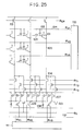
- Fig. 25 is a diagram showing best the feature of the eleventh embodiment.
- Numeral 301 represents a MOS transistor switch.
- MOS transistor switch 301 when the MOS transistor switch 301 is turned on in response to ⁇ G to operate at the timing shown in Fig. 24, an addition of the 2 x 3 pixel signal can be derived.
- MOS transistor switch 301 When the MOS transistor switch 301 is turned off in response to ⁇ G to operate at the timing shown in Fig. 26, each pixel signal can be read sequentially.
- Fig. 22 is a drawing indicating best the feature of the twelfth embodiment.
- Numeral 401 represents a clamp capacitance and 402 represents a reset MOS transistor.
- the reset is made to a fixed potential by turning on the reset MOS transistor 402 while the emitter reset voltage is read out at the timing t e before the sensor signal reading time. Then since the output can be read out, the fixed variations occurring in each reading system, for example, offset variations in the amplifier unit, is removed, whereby the output can be obtained with higher accuracy.
- the reading amplifier should not be limited to the above mode.
- the amplifier may includes P-channel MOS transistors (Fig. 29A) or bipolar transistors (Fig. 29B).
- the resistor should not be limited to a fixed resistor.
- the amplification-type sensor should not be limited to BASIS.
- the same effect can be obtained using charge modulation devices (CMDs) or MOS-type amplification-type photoelectric conversion elements.
- the present embodiment described above is effective in case where it is desired to recognize the average signal level of an image area to execute a signal process in response to a signal from a sensor, or to recognize a rough distribution in signal amount of an image area to execute a detail signal process to a specific area.
- the conventional sensor in order to examine the detail distribution in signal amount after the darkest area in an image area has been roughly extracted, the conventional sensor must execute a sophisticated image process. It is necessary to perform the above averaging process and an area division after all signals of an image area have been once stored in a memory in a signal processing system. Hence such a process makes the signal processing system complicated and large, thus taking a relatively long processing time.
- means is arranged, which adds and outputs signals from plural pixels in response to an external simple pulse to the signal reading portion in a sensor, and then supplies the output to the signal processing system.
- the information processing system can be more simplified, whereby the processing time can be shortened.
- preparing the means for adding and outputting signals from plural signal sources allows the signal processor to be further simplified and miniaturized, thus decreasing the signal processing time.
Landscapes
- Engineering & Computer Science (AREA)
- Multimedia (AREA)
- Signal Processing (AREA)
- Transforming Light Signals Into Electric Signals (AREA)
Claims (9)
- Processeur de signaux, comportant :au moins quatre sources de signaux définissant une zone d'image (S1, S2, S3, S4) ;plusieurs moyens de blocage de signaux (C11, ... C14) destinés à bloquer des signaux de sortie desdites sources de signaux ;des moyens (11', 2', 5', 10') de mélange de signaux destinés à mélanger au moins deux signaux distincts parmi des signaux de sortie bloqués par ladite pluralité de moyens de blocage de signaux pour produire au moins deux signaux mélangés ; etdes moyens (11, 2, 5, 10) de sortie de signaux distincts destinés à produire respectivement les signaux de sortie à partir de ladite pluralité de sources de signaux, et caractérisé en ce que lesdits moyens de sortie de signaux distincts sont agencés de façon à lire une zone limitée à l'intérieur de ladite zone d'image après qu'une allure d'image entière de ladite zone d'image a été lue sur la base desdits signaux mélangés.
- Processeur de signaux selon la revendication 1, dans lequel chacun desdits moyens de blocage de signaux comprend un élément à capacité (C11, ... C14).
- Processeur de signaux selon la revendication 2, dans lequel chacun desdits moyens de blocage de signaux comprend un élément de capacité variable.
- Processeur de signaux selon l'une quelconque des revendications 1 à 3, dans lequel chacune des sources de signaux comprend un élément de conversion photoélectrique.
- Processeur de signaux selon l'une quelconque des revendications précédentes, comportant en outre un amplificateur agencé entre lesdites sources de signaux et lesdits moyens de blocage de signaux.
- Processeur de signaux selon la revendication 5, dans lequel ledit amplificateur comprend un circuit destiné à produire un niveau différentiel entre ledit signal de sortie d'une source de signal correspondant et un signal de référence.
- Processeur de signaux selon l'une quelconque des revendications précédentes, dans lequel lesdits moyens de mélange de signaux comprennent un commutateur qui connecte au moins deux desdits moyens de blocage de signaux l'un à l'autre, et un circuit de balayage (11') destiné à balayer les moyens de blocage de signaux lorsqu'ils sont connectés par ledit commutateur, et dans lequel lesdits moyens de sortie de signaux distincts comprennent un commutateur agencé de façon à être associé à chacun desdits moyens de blocage de signaux, et un second circuit de balayage (11) destiné à balayer successivement les moyens de blocage.
- Processeur de signaux selon la revendication 7, dans lequel lesdits moyens de sortie de signaux distincts sélectionnent un signal distinct devant être délivré en sortie sur la base d'une information obtenue par lesdits moyens de mélange de signaux.
- Processeur de signaux selon la revendication 7, dans lequel un nombre prédéterminé de sources de signaux parmi ladite pluralité de sources de signaux est destiné à délivrer en sortie des signaux distincts basés sur lesdits signaux mélangés après que lesdits moyens de mélange de signaux ont délivré en sortie des signaux à partir de la totalité de ladite pluralité de sources de signaux.
Applications Claiming Priority (4)
| Application Number | Priority Date | Filing Date | Title |
|---|---|---|---|
| JP53894/93 | 1993-03-15 | ||
| JP05389493A JP3437208B2 (ja) | 1993-03-15 | 1993-03-15 | 信号処理装置 |
| JP5095988A JPH06311439A (ja) | 1993-04-22 | 1993-04-22 | 信号処理装置 |
| JP95988/93 | 1993-04-22 |
Publications (3)
| Publication Number | Publication Date |
|---|---|
| EP0616464A2 EP0616464A2 (fr) | 1994-09-21 |
| EP0616464A3 EP0616464A3 (fr) | 1995-01-18 |
| EP0616464B1 true EP0616464B1 (fr) | 1999-06-02 |
Family
ID=26394619
Family Applications (1)
| Application Number | Title | Priority Date | Filing Date |
|---|---|---|---|
| EP94301799A Expired - Lifetime EP0616464B1 (fr) | 1993-03-15 | 1994-03-14 | Processeur de signal |
Country Status (3)
| Country | Link |
|---|---|
| US (1) | US5867045A (fr) |
| EP (1) | EP0616464B1 (fr) |
| DE (1) | DE69418754T2 (fr) |
Families Citing this family (10)
| Publication number | Priority date | Publication date | Assignee | Title |
|---|---|---|---|---|
| JP3385760B2 (ja) * | 1994-02-21 | 2003-03-10 | ソニー株式会社 | 固体撮像装置及びその駆動方法 |
| EP0725535B1 (fr) * | 1995-02-01 | 2003-04-23 | Canon Kabushiki Kaisha | Dispositif de prise de vues à l'état solide et son procédé de mise en oeuvre |
| EP0777379B1 (fr) * | 1995-11-21 | 2002-02-20 | STMicroelectronics S.r.l. | Capteur optique adaptatif |
| US6847399B1 (en) | 1998-03-23 | 2005-01-25 | Micron Technology, Inc. | Increasing readout speed in CMOS APS sensors through block readout |
| US6239456B1 (en) | 1998-08-19 | 2001-05-29 | Photobit Corporation | Lock in pinned photodiode photodetector |
| FI106415B (fi) * | 1998-12-22 | 2001-01-31 | Nokia Mobile Phones Ltd | Parannettu menetelmä ja piirijärjestely signaalin käsittelemiseksi |
| JP4846186B2 (ja) * | 2001-03-29 | 2011-12-28 | ギブン イメージング リミテッド | タイミング制御のための方法 |
| JP2002330349A (ja) * | 2001-04-26 | 2002-11-15 | Fujitsu Ltd | Xyアドレス型固体撮像装置 |
| US7408683B2 (en) * | 2002-07-15 | 2008-08-05 | Brother Kogyo Kabushiki Kaisha | Image sensor for reading image and image reading apparatus including the image sensor |
| JP2005348041A (ja) * | 2004-06-02 | 2005-12-15 | Canon Inc | 固体撮像装置および撮像システム |
Family Cites Families (15)
| Publication number | Priority date | Publication date | Assignee | Title |
|---|---|---|---|---|
| US4001605A (en) * | 1975-09-29 | 1977-01-04 | The Bendix Corporation | Voter circuit including averaging means |
| JPS583630B2 (ja) * | 1977-09-16 | 1983-01-22 | 松下電子工業株式会社 | 固体光像検出装置 |
| FI63635C (fi) * | 1981-06-22 | 1983-07-11 | Instrumentarium Oy | Filtrationsarrangemang foer eliminering av naetstoerningar |
| US4686554A (en) * | 1983-07-02 | 1987-08-11 | Canon Kabushiki Kaisha | Photoelectric converter |
| JPS6181087A (ja) * | 1984-09-28 | 1986-04-24 | Olympus Optical Co Ltd | 固体撮像装置 |
| US4616142A (en) * | 1984-12-31 | 1986-10-07 | Sundstrand Corporation | Method of operating parallel-connected semiconductor switch elements |
| ATE163498T1 (de) * | 1985-11-15 | 1998-03-15 | Canon Kk | Photoelektrische wandlervorrichtung |
| FR2598019B1 (fr) * | 1986-04-25 | 1992-09-11 | Thomson Csf | Procede d'utilisation d'une matrice photosensible a transfert de charge, et matrice photosensible ainsi utilisee |
| JPH0644619B2 (ja) * | 1986-07-17 | 1994-06-08 | キヤノン株式会社 | 光電変換装置 |
| JPH0693615B2 (ja) * | 1988-05-16 | 1994-11-16 | 株式会社東芝 | ドライバ回路 |
| US4996413A (en) * | 1990-02-27 | 1991-02-26 | General Electric Company | Apparatus and method for reading data from an image detector |
| JP3016815B2 (ja) * | 1990-04-27 | 2000-03-06 | キヤノン株式会社 | 固体撮像装置 |
| US5166539A (en) * | 1990-07-09 | 1992-11-24 | Nippon Telegraph And Telephone Corporation | Neural network circuit |
| FR2672989A1 (fr) * | 1991-02-15 | 1992-08-21 | Sodern | Dispositif de determination de la direction d'une source emissive de faible luminosite et son application a la visee stellaire. |
| DE4123203C1 (en) * | 1991-07-13 | 1992-10-29 | Eligiusz Dipl.-Ing. 7538 Keltern De Wajda | Solid state image converter - has radiation sensitive surface with regions of various densities of distribution of elements i.e. of different levels of resolution |
-
1994
- 1994-03-14 EP EP94301799A patent/EP0616464B1/fr not_active Expired - Lifetime
- 1994-03-14 DE DE69418754T patent/DE69418754T2/de not_active Expired - Lifetime
-
1996
- 1996-11-19 US US08/744,838 patent/US5867045A/en not_active Expired - Lifetime
Also Published As
| Publication number | Publication date |
|---|---|
| EP0616464A2 (fr) | 1994-09-21 |
| EP0616464A3 (fr) | 1995-01-18 |
| DE69418754T2 (de) | 1999-11-04 |
| DE69418754D1 (de) | 1999-07-08 |
| US5867045A (en) | 1999-02-02 |
Similar Documents
| Publication | Publication Date | Title |
|---|---|---|
| US7755690B2 (en) | Solid state image sensor with fixed pattern noise reduction | |
| EP0809300B1 (fr) | Capteur d'images à éléments d'image actifs avec remise à zéro individuelle des éléments d'image | |
| JP2884205B2 (ja) | 固体撮像装置 | |
| KR101177140B1 (ko) | 고체 촬상 장치, 고체 촬상 장치의 구동 방법 및 촬상 장치 | |
| EP0272152B1 (fr) | Circuit de lecture de signal | |
| EP0576104B1 (fr) | Appareil de conversion photo-électrique | |
| EP1178673A2 (fr) | Dispositif de prise d'images à l'état solide | |
| EP0905787B1 (fr) | Capteur d'image à l'état solide et sa méthode de commande | |
| US20040051802A1 (en) | Differential readout from pixels in CMOS sensor | |
| US7116367B2 (en) | Solid-state image pickup apparatus having a reset transistor controlled by an output line | |
| JP3544084B2 (ja) | 増幅型固体撮像装置 | |
| US20040201550A1 (en) | Biasing scheme for large format CMOS active pixel sensors | |
| US4910597A (en) | Photoelectric converting apparatus accumulating a readout signal and a remaining signal | |
| US5796431A (en) | Solid-state image pickup device and driving method thereof | |
| EP0616464B1 (fr) | Processeur de signal | |
| JP2001045375A (ja) | 撮像装置とその読み出し方法 | |
| US6781627B1 (en) | Solid state imaging device and electric charge detecting apparatus used for the same | |
| US7068315B1 (en) | Solid-state imaging device, its driving method, and camera system | |
| JP2001008109A (ja) | 固体撮像素子およびその駆動方法並びにカメラシステム | |
| JP3437208B2 (ja) | 信号処理装置 | |
| JP2000324397A (ja) | 固体撮像素子 | |
| JP2897106B2 (ja) | 固体撮像装置 | |
| US7012238B2 (en) | Amplification-type solid-state image pickup device incorporating plurality of arrayed pixels with amplification function | |
| JP2000188723A (ja) | 画像処理装置 | |
| JPH11239299A (ja) | 固体撮像装置及びその駆動方法、並びにカメラ |
Legal Events
| Date | Code | Title | Description |
|---|---|---|---|
| PUAI | Public reference made under article 153(3) epc to a published international application that has entered the european phase |
Free format text: ORIGINAL CODE: 0009012 |
|
| AK | Designated contracting states |
Kind code of ref document: A2 Designated state(s): DE FR GB IT NL |
|
| PUAL | Search report despatched |
Free format text: ORIGINAL CODE: 0009013 |
|
| AK | Designated contracting states |
Kind code of ref document: A3 Designated state(s): DE FR GB IT NL |
|
| 17P | Request for examination filed |
Effective date: 19950606 |
|
| 17Q | First examination report despatched |
Effective date: 19961212 |
|
| GRAG | Despatch of communication of intention to grant |
Free format text: ORIGINAL CODE: EPIDOS AGRA |
|
| GRAG | Despatch of communication of intention to grant |
Free format text: ORIGINAL CODE: EPIDOS AGRA |
|
| GRAH | Despatch of communication of intention to grant a patent |
Free format text: ORIGINAL CODE: EPIDOS IGRA |
|
| GRAH | Despatch of communication of intention to grant a patent |
Free format text: ORIGINAL CODE: EPIDOS IGRA |
|
| GRAA | (expected) grant |
Free format text: ORIGINAL CODE: 0009210 |
|
| AK | Designated contracting states |
Kind code of ref document: B1 Designated state(s): DE FR GB IT NL |
|
| REF | Corresponds to: |
Ref document number: 69418754 Country of ref document: DE Date of ref document: 19990708 |
|
| ET | Fr: translation filed | ||
| PLBE | No opposition filed within time limit |
Free format text: ORIGINAL CODE: 0009261 |
|
| STAA | Information on the status of an ep patent application or granted ep patent |
Free format text: STATUS: NO OPPOSITION FILED WITHIN TIME LIMIT |
|
| 26N | No opposition filed | ||
| REG | Reference to a national code |
Ref country code: GB Ref legal event code: IF02 |
|
| PGFP | Annual fee paid to national office [announced via postgrant information from national office to epo] |
Ref country code: FR Payment date: 20100414 Year of fee payment: 17 |
|
| PGFP | Annual fee paid to national office [announced via postgrant information from national office to epo] |
Ref country code: NL Payment date: 20100315 Year of fee payment: 17 Ref country code: IT Payment date: 20100329 Year of fee payment: 17 |
|
| REG | Reference to a national code |
Ref country code: NL Ref legal event code: V1 Effective date: 20111001 |
|
| REG | Reference to a national code |
Ref country code: FR Ref legal event code: ST Effective date: 20111130 |
|
| PG25 | Lapsed in a contracting state [announced via postgrant information from national office to epo] |
Ref country code: FR Free format text: LAPSE BECAUSE OF NON-PAYMENT OF DUE FEES Effective date: 20110331 Ref country code: NL Free format text: LAPSE BECAUSE OF NON-PAYMENT OF DUE FEES Effective date: 20111001 |
|
| PG25 | Lapsed in a contracting state [announced via postgrant information from national office to epo] |
Ref country code: IT Free format text: LAPSE BECAUSE OF NON-PAYMENT OF DUE FEES Effective date: 20110314 |
|
| PGFP | Annual fee paid to national office [announced via postgrant information from national office to epo] |
Ref country code: DE Payment date: 20120331 Year of fee payment: 19 |
|
| PGFP | Annual fee paid to national office [announced via postgrant information from national office to epo] |
Ref country code: GB Payment date: 20120223 Year of fee payment: 19 |
|
| GBPC | Gb: european patent ceased through non-payment of renewal fee |
Effective date: 20130314 |
|
| REG | Reference to a national code |
Ref country code: DE Ref legal event code: R119 Ref document number: 69418754 Country of ref document: DE Effective date: 20131001 |
|
| PG25 | Lapsed in a contracting state [announced via postgrant information from national office to epo] |
Ref country code: GB Free format text: LAPSE BECAUSE OF NON-PAYMENT OF DUE FEES Effective date: 20130314 Ref country code: DE Free format text: LAPSE BECAUSE OF NON-PAYMENT OF DUE FEES Effective date: 20131001 |