EP0617552A2 - Capteur d'images à état solide - Google Patents
Capteur d'images à état solide Download PDFInfo
- Publication number
- EP0617552A2 EP0617552A2 EP94104595A EP94104595A EP0617552A2 EP 0617552 A2 EP0617552 A2 EP 0617552A2 EP 94104595 A EP94104595 A EP 94104595A EP 94104595 A EP94104595 A EP 94104595A EP 0617552 A2 EP0617552 A2 EP 0617552A2
- Authority
- EP
- European Patent Office
- Prior art keywords
- signal
- pixel
- sample
- state imaging
- imaging device
- Prior art date
- Legal status (The legal status is an assumption and is not a legal conclusion. Google has not performed a legal analysis and makes no representation as to the accuracy of the status listed.)
- Granted
Links
Images

Classifications
-
- H—ELECTRICITY
- H04—ELECTRIC COMMUNICATION TECHNIQUE
- H04N—PICTORIAL COMMUNICATION, e.g. TELEVISION
- H04N25/00—Circuitry of solid-state image sensors [SSIS]; Control thereof
- H04N25/60—Noise processing, e.g. detecting, correcting, reducing or removing noise
- H04N25/67—Noise processing, e.g. detecting, correcting, reducing or removing noise applied to fixed-pattern noise, e.g. non-uniformity of response
Definitions
- the present invention relates to solid-state imaging devices and, more particularly, to an amplifying type solid-state imaging device in which a fixed pattern noise (FPN) can be canceled from a video signal formed from a pixel (i.e., pixel signal).
- FPN fixed pattern noise
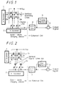
- FIG. 1 of the accompanying drawings shows an example of a conventional amplifying type solid-state imaging device.
- MOS transistors Qe, Qe, ... each having an annular-shaped gate, form pixels.
- the MOS transistors Qe, Qe, ... are arranged in a matrix of rows and columns (i.e., in a two-dimensional fashion).
- Each of the MOS transistors Qe, Qe, ... has an annular-shaped gate.
- a drain provided at the outside of the annular-shaped gate of the MOS transistor Qe is connected to a power supply (V DD line) and a source provided at the inside of the annular-shaped gate of the MOS transistor Qe is connected to signal lines.
- the annular-shaped gate of the MOS transistor Qe is connected to vertical scanning lines.
- the annular-shaped gate is made of thin transparent polysilicon, and a channel current of the MOS transistors Qe, Qe, ... is modulated by photoelectrically converting light incident on the channel through the angular-shaped gate.
- Horizontal switching transistors Qh, Qh, ... are connected between signal lines associated with vertical columns of pixels and output line in order to effect the horizontal scanning.
- a vertical scanner (vertical scanning circuit) 1 is adapted to scan horizontal rows of the pixels that are arranged in a matrix fashion.
- a horizontal scanner (horizontal scanning circuit) 2 is adapted to control the horizontal switching transistors Qh, Qh, ...
- a signal of pixel which belongs to the horizontal row scanned by the vertical scanner 1 and which belongs to the column scanned by the horizontal scanner 2 is outputted to the outside as an output signal of the amplifying type solid-state imaging device.
- An analog-to-digital (A/D) converter 3 is provided in the outside of the amplifying type solid-state imaging device.
- the A/D converter 3 converts an output pixel signal from the amplifying type solid-state imaging device into a digital signal.
- a frame memory 4 is adapted to store therein one frame of the output signal from the A/D converter 3. More specifically, the frame memory 4 stores therein one frame of the output signal from the A/D converter 3 in order to cancel a noise signal (fixed pattern noise).
- the fixed pattern noise will be referred to hereinafter as "FPN" for simplicity.
- a subtracter 5 subtracts the signal (noise signal) outputted from the frame memory 4 from the digital signal (pixel signal) outputted from the A/D converter 3.
- the frame memory 4 stores therein one frame of a pixel signal (corresponding to an FPN signal, i.e., noise signal) obtained when the whole of the amplifying type solid-state imaging device is shielded from light from the outside. If the pixel signal is outputted from the A/D converter 3 when light becomes incident on the amplifying type solid-state imaging device normally, then the noise signal of the pixel of the pixel signal is read out from the frame memory 4 and the FPN is canceled by subtracting the noise signal from the pixel signal of the same pixel by the subtracter 5.
- an FPN signal i.e., noise signal
- FIG. 2 is a schematic diagram showing an arrangement of another example of the conventional amplifying type solid-state imaging device.
- the FPN that occurred in the pixel Tr is canceled by CDS (correlated double sampling) circuits 20 provided between the horizontal switching transistors Qh and the signal lines. Also, the FPN generated by the CDS circuit 20 is canceled by subtracting the FPN from the pixel signal.
- the frame memory 4 shown in FIG. 1 is replaced with a line memory 4a.
- the line memory 4a stores therein an optical black signal of one horizontal line portion in a vertical optical black row (not shown) during a vertical optical blanking period as a noise signal.
- the amplifying type solid-state imaging device shown in FIG. 1 needs the frame memory 4 having a storage capacity large enough to store therein the noise signal of one frame. Further, this solid-state imaging device needs the A/D converter 3 to digitize the output pixel signal so that the output pixel signal may be stored in the frame memory 4. There is then the problem that the amplifying type solid-state imaging device cannot be made inexpensive. Furthermore, there is the problem that the noise signal of one frame should be stored in the frame memory 4 each time the cameraman takes a picture.
- the amplifying type solid-state imaging device shown in FIG. 2 needs the line memory 4a having a storage capacity of one horizontal line amount though this storage capacity of the line memory 4a is not so large as that of the frame memory 4.
- the amplifying type solid-state imaging device shown in FIG. 2 also needs the A/D converter 3 and therefore cannot be made inexpensive satisfactorily.
- the amplifying type solid-state imaging device shown in FIG. 2 need not store the noise signal unlike the amplifying type solid-state imaging device shown in FIG. 1 and the noise signal is automatically written in the line memory 4a at every frame so as to cancel the FPN
- the amplifying type solid-state imaging device shown in FIG. 2 has the problem that FPNs which are different at every pixel cannot be canceled out completely because FPNs of all horizontal lines are canceled by the optical black signal of one horizontal line regardless of the fact that FPNs are subtly different in every horizontal line.
- U.S. patent No. 4,914,519 describes a photoelectric-conversion apparatus in which sample and hold circuits sample and hold a signal read out from the same photoelectric converting element and a refreshed remaining signal and a noise is canceled by effecting a subtraction on the above two signals.
- FPN fixed pattern noise
- a solid-state imaging device which is comprised of a plurality of pixels arranged in a matrix of rows and columns, each pixel converting incident light into a pixel signal, vertical scanning lines associated with rows of the pixels, vertical signal lines, associated with columns of the pixels, for respectively outputting the pixel signal, first and second sample and hold circuits associated with each of the vertical signal lines, the sample and hold circuits sampling and holding the pixel signal and a noise signal alternately, and a subtracter associated to the first and second sample and hold circuits through first switching means so that an output of the first and second sample and hold circuits is inputted to a first input terminal of the subtracter when the noise signal is outputted, and is inputted to a second input terminal of the subtracter when the pixel signal is outputted to thereby obtain an output signal by subtracting the noise signal from the pixel signal.
- the pixel signal and the noise signal from the same pixel are sampled and held by the same sample and hold circuit of the first and second sample and hold circuits.
- the first and second sample and hold circuits sample and hold the pixel signal and the noise signal alternately at every horizontal scanning period so that a pixel signal and a noise signal to be sampled and held during the same horizontal scanning period are generated from different pixels.
- the first and second sample and hold circuits and the subtracter have amplifying means and second switching means connected therebetween.
- the vertical signal lines are grounded through load means.
- the pixel includes an MOS transistor having a gate connected to the vertical scanning lines, a source connected to the vertical signal lines and a drain connected to a power supply.
- the MOS transistor is arranged such that a channel current is modulated on the basis of an amount of electric charges which are accumulated under the gate thereof by photoelectric conversion.
- a solid-state imaging device which is comprised of a plurality of pixels arranged in a matrix of rows and columns, each pixel converting incident light into a pixel signal, vertical scanning lines associated with rows of the pixels, vertical signal lines, associated with columns of the pixels, for respectively outputting the pixel signal, a first sample and hold circuit for sampling and holding a pixel signal and being associated to a first output line, a second sample and hold circuit for sampling and holding a noise signal after resetting the pixel and being associated to a second output line, and a subtracter for receiving an output of the first and second sample and hold circuits through the first and second output lines to thereby obtain an output signal by subtracting the noise signal from said pixel signal.
- the vertical signal lines are grounded through load means.
- the pixel includes an MOS transistor having a gate connected to the vertical scanning lines, a source connected to the vertical signal lines and a drain connected to a power supply.
- the MOS transistor is arranged such that a channel current is modulated on the basis of an amount of electric charges which are accumulated under the gate thereof by photoelectric conversion.
- a solid-state imaging device which is comprised of a plurality of pixels arranged in a matrix of rows and columns, each pixel converting incident light into a pixel signal, vertical scanning lines associated with rows of pixels, vertical signal lines, associated with columns of the pixels, for respectively outputting the pixel signal, first and second sample and hold means connected to the vertical signal lines in parallel to each other and sampling and holding the pixel signal and a noise signal alternately, and sampling and holding different signals of the pixel signal and the noise signal during the same horizonal scanning period, means for delaying an output of the pixel signal from the first sample and hold circuit by one horizontal scanning period and outputting the delayed pixel signal, and a subtracter connected to the first and second sample and hold circuits and subtracting a noise signal from an output of the delayed pixel signal.
- the pixel signal and the noise signal of the same pixel are sampled and held by the same sample and hold circuit.
- the solid-state imaging device of the present invention since the pixel signal and the noise signal of the same pixel outputted from the first and second sample and hold circuits are simultaneously inputted to the subtracter which then subtracts the noise signal from the pixel signal, the FPN (fixed pattern noise) of each pixel can be canceled accurately and reliably. Thus, even when the FPN between the pixels is fluctuated, it is possible to obtain an accurate pixel signal, i.e., a pixel signal which precisely corresponds to the amount of light incident on the pixel.
- the solid-state imaging device of the present invention since the pixel signal and the noise signal are sampled and held by the same sample and hold circuit without fail, the FPN in the sample and hold circuit can be prevented from being mixed into the pixel signal and a more accurate noise signal can be obtained.
- the solid-state imaging device of the present invention even when the pixel signal and the noise signal that are sampled and held by the first and second sample and hold circuits during the same horizontal scanning period are generated from other pixel, the pixel signal and the noise signal of the same pixel can simultaneously be inputted to the subtracter by alternately sampling and holding the pixel signal and the noise signal by the first and second sample and hold circuits and by delaying the pixel signal, and the FPN can be canceled.
- the solid-state imaging device of the present invention since the first sample and hold circuit samples and holds the pixel signal and the second sample and hold circuit samples and holds the noise signal and the pixel signal and the noise signal are simultaneously inputted to the subtracter through the first and second output lines, it is possible to remove the switching means that is used to input the pixel signal and the noise signal of the same pixel to the subtracter at the same time.
- the solid-state imaging device of the present invention since the two signals from the first and second sample and hold circuits are switched by the second switching means and amplified by one amplifying means, an S/N can be improved and the subtracter can subtract the noise signal from the pixel signal. Moreover, because the subtracted pixel signal and the subtraction noise signal are amplified by the same amplifying means, the FPN in the amplifying means can be prevented from being mixed into the pixel signal.
- the MOS transistor which forms the pixel and the load means constitute the source-follower circuit, thereby the output impedance being lowered.
- the solid-state imaging device of the present invention can be applied to a solid-state imaging device of the type such that the pixel is formed of the MOS transistor.
- the solid-state imaging device of the present invention can be applied to the amplifying type solid-state imaging device.
- FIG. 3 shows a solid-state imaging device according to a first embodiment of the present invention.
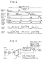
- FIG. 4 is a timing chart used to explain operation of the first embodiment according to the present invention.
- the solid-state imaging device according to the present invention has features different from and common to those of the prior-art solid-state imaging devices shown in FIGS. 1 and 2.
- the features common to the conventional solid-state imaging devices shown in FIGS. 1 and 2 have been described so far and therefore only the different features of the solid-state imaging device shown in FIG. 3 will be described below in detail.
- first and second sample and hold circuits 6a S/1H
- 6b S/2H
- sample and hold signals in response to sample control pulses ⁇ SH1, ⁇ SH2 supplied thereto.
- the other ends of the sample and hold circuits 6a, 6b are connected to one ends of the horizontal switching transistors Qh, Qh.
- An output signal from the first sample and hold circuit 6a is transmitted through one horizontal switching transistor Qh to a first output line as a first output signal Out1.
- An output signal from the second sample and hold circuit 6b is transmitted through the other horizontal switching transistor Qh to a second output line as a second output signal Out2.
- sample and hold circuit 6 sample and hold circuits 6a, 6b are collectively referred to hereinafter as a sample and hold circuit 6 when necessary
- the horizontal switching transistor Qh at every vertical signal line.
- two output lines also are provided.
- Load transistors Ql, Ql, ..., are connected between the respective vertical signal lines and the ground to thereby cause the MOS transistor Qe forming the pixel to operate in a source-follower circuit fashion.
- the solid-state imaging device is different from the conventional amplifying type solid-state imaging devices shown in FIGS. 1, 2 in that the two output signals Out1, Out2 from the amplifying solid-state imaging device are amplified by AGC (automatic gain control) amplifiers 7a, 7b and inputted through a so-called swap switch 8 to a 1H delay line 9 and a subtracter 10.
- AGC automatic gain control
- the swap switch 8 repeats a switching operation at every two horizontal periods in such a manner as to transmit the first output signal Out1 to the 1H delay line 9 and to transmit the second output signal Out2 to the subtracter 10 during one horizontal period and to transmit the second output signal Out2 to the 1H delay line 9 and to transmit the first output signal Out1 to the subtracter 10 during the next horizontal period.
- An output signal from the 1H delay line 9 is inputted to the plus-side input terminal of the subtracter 10 and the output signal that is directly transmitted from the swap switch 8 to the subtracter 10 is inputted to the minus-side input terminal of the subtracter 10.
- selection pulses ⁇ V n , ⁇ V n-1 are held at middle level during the last one third period of the horizontal blanking period of the horizontal period, whereby a signals is read out from nth and n-1th rows of the pixel.
- the signal thus read out includes both of a pixel signal and a noise signal.
- the signal thus read out is sampled and held by the first sample and hold circuit 6a (S/H1) at a timing of the sample control pulse ⁇ SH1 during the horizontal blanking period, and then outputted from a first output line through the horizontal switching transistor Qh driven by the horizontal scanner 2 during the effective period of the horizontal scanning period.
- This output signal is expressed as S(n, n-1) in FIG. 4.
- This signal is inputted to the 1H delay means 9 through the swap switch 8 from the amplifier 7a.
- the selection pulses ⁇ V n , ⁇ V n-1 are held at high level and the pixel is reset. Then, the selection pulses ⁇ V n , ⁇ V n-1 are held at middle level to read out a dark signal, i.e., noise signal, whereafter the pulses ⁇ V n , ⁇ V n-1 are held at low level.
- the sample control pulse ⁇ SH1 is outputted during the dark signal is read out, and allows the first sample and hold circuit 6a (S/1H) to sample the signal of nth and n+1th rows of the pixel, i.e., noise signal N(n, n+1),
- the noise signal N(n, n+1) is output from the amplifying type solid-state imaging device as the first output signal Out1 during the effective period and the swap switch 8 is changed in position at every horizonal period through the AGC amplifier 7b, the noise signal N(n, n+1) is inputted to the minus-side input terminal of the subtracter 10.
- the subtracter 10 is supplied at its plus-side input terminal with the pixel signal (i.e., pixel signal containing a noise signal strictly speaking) S(n, n-1) inputted to the 1H delay line 9 one horizontal period before and is also supplied at its minus-side input terminal with a noise signal N(n, n-1), to thereby carry out a subtraction of S(n, n-1) - N(n, n-1).
- the subtracter 10 outputs a pixel signal from which a noise signal of nth and n-1th rows of the pixel, i.e., FPN is canceled.
- the second sample and hold circuit 6b is operated as follows.
- the second sample and hold circuit 6b samples and holds a noise signal N(n-3, n-2) of n-3th and n-2th rows of the pixel. Then, the noise signal N(n-3, n-2) is inputted through the AGC amplifier 7b and the swap switch 8 to the minus-side input terminal of the subtracter 10, in which it is subtracted from a pixel signal S(n-3, n-2) that has been inputted to the 1H delay line 9 at every horizontal period. As a consequence, the solid-state imaging device outputs a pixel signal from which a noise signal of n-3 and n-2th rows of the pixel is canceled.
- the second sample and hold circuits 6b samples and holds a pixel signal of S(n+1, n+2) of n+1th and n+2th rows of the pixel.
- the other sample and hold circuit 6 samples and holds the noise signal N of the pixel different from that of the pixel signal S. Then, when the sample and hold circuits 6a, 6b are assumed to be the same sample and hold circuit 6, the sample and hold circuit 6 samples and holds the pixel signal S of a pair of rows in one horizontal period and samples and holds the noise signal N of the same rows in the next horizontal period. The above operation is repeated by the sample and hold circuit 6.
- the pixel signal from each pixel can be outputted under the condition that the noise signal of each pixel is canceled therefrom. Moreover, since the pixel signal and the noise signal of the same row are processed by the same sample and hold circuit 6, a characteristic difference between the first and second sample and hold circuits 6a, 6b can be prevented from being mixed into the pixel signal, i.e., the FPN of the sample and hold circuit 6 also can be canceled. Therefore, the FPN can be canceled perfectly.
- FIG. 5 is a circuit diagram showing a main portion of a modified example of the solid state imaging device shown in FIG. 3.
- the first and second output signals Out1 and Out2 are amplified by a single AGC amplifier 7 in a time-division manner.
- a contrast difference can be prevented from being produced between the scanning lines due to a gain difference between the AGC amplifiers 7a and 7b shown in FIG. 3.
- the level of the signal should preferably be raised in order to increase an S/N (signal-to-noise ratio) so that a random noise that is increased by the subtraction processing may become negligibly small.
- the AGC amplifiers 7a, 7b are provided in order to raise the level of the signal as described above. It is, however, unavoidable that the two AGC amplifiers 7a, 7b have a gain difference therebetween even though they are manufactured similarly.
- the two signals Out1, Out2 from the amplifying type solid-state imaging device are amplified by the AGC amplifier 7.
- Switches (second switching means) 11a, 11b are connected to the front and rear stages of the AGC amplifier 7 so as to change in position to the first output Out1 side or the second output Out2 side so that the AGC amplifier 7 can be operated to amplify the signal in a time division manner.
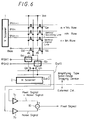
- FIG. 6 is a diagram showing an arrangement of the solid-state imaging device according to the second embodiment of the present invention.
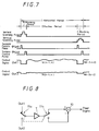
- FIG. 7 is a timing chart used to explain operation of the second embodiment of the present invention.
- the second embodiment shown in FIG. 6 is exactly the same as the first embodiment shown in FIG. 3 in circuit arrangement of the amplifying type solid-state imaging device. However, the second embodiment is different from the first embodiment in circuit arrangement and operation of the external circuit of the amplifying type solid-state imaging device.
- the first output signal Out1 from the first sample and hold circuit 6a is inputted through the AGC amplifier 7a to the plus-side input terminal of the subtracter 10.
- the second output signal Out2 from the second sample and hold circuit 6b is inputted through the AGC amplifier 7b to the minus-side input terminal of the subtracter 10.
- the first and second sample and hold circuits 6a, 6b sample and hold the pixel signal and the noise signal of the same pixel at the same time.
- the pixel signal S(n-1, n) of selected rows e.g., n-1th and nth rows is read out.
- the first sample and hold circuit 6a samples and holds the pixel signal S(n-1, n) in response to the sample control pulse ⁇ SH1 supplied thereto.
- the pixel of the n-1th and nth rows is reset and then the noise signal N(n-1, n) is read out.
- the second sample and hold circuit 6b samples and holds the noise signal N(n-1, n) in response to the sample control pulse ⁇ SH2 supplied thereto.
- the pixel signal S(n-1, n) and the noise signal N(n-1, n) are outputted simultaneously, i.e., the pixel signal and the noise signal of the same rows (n-1, n) of the pixel are outputted and then inputted to the subtracter 10. Consequently, the signal of the pixel signal S - noise signal N is outputted from the subtracter 10 as the pixel signal, i.e., the pixel signal whose FPN is canceled is outputted from the subtracter 10.
- the solid-state imaging device of this embodiment does not need the 1H delay line 9 and the swap switch 8.
- FIG. 8 shows a main portion of a modified example of the second embodiment shown in FIG. 6.
- the first and second output signals Out1, Out2 are amplified by the single AGC amplifier 7 in a time division manner in exactly the same way as that of the modified example shown in FIG. 5.
- the switches 11a, 11b are connected to the front and rear stage of the AGC amplifier 7 so as to change in position to the first output signal Out1 side or the second output signal Out2 side so that the AGC amplifier 7 may amplify the first and second output signals Out1, Out2 in a time division manner.
- one ends of the first and second sample and hold circuits are connected to the vertical signal lines.
- the subtracter is connected to the rear stage of the sample and hold circuits through the switching means. The subtracter subtracts the noise signal outputted from one of the first and second sample and hold circuit from the pixel signal outputted from the other of the first and second sample and hold circuit.
- the solid-state imaging device of the present invention since the pixel signal and the noise signal of the same pixel outputted from the first and second sample and hold circuits are simultaneously inputted to the subtracter which then subtracts the noise signal from the pixel signal, the FPN (fixed pattern noise) of each pixel can be canceled accurately and reliably. Thus, even when the FPN between the pixels is fluctuated, it is possible to obtain an accurate pixel signal, i.e., a pixel signal which precisely corresponds to the amount of light incident on the pixel.
- the solid-state imaging device of the present invention since the pixel signal and the noise signal are sampled and held by the same sample and hold circuit without fail, the FPN in the sample and hold circuit can be prevented from being mixed into the pixel signal and a more accurate noise signal can be obtained,
- the first and second sample and hold circuits sample and hold the pixel signal and the noise signal at every horizontal scanning period alternately so that the pixel signal and the noise signal that were sampled and held during the same horizontal scanning period are generated from other pixel.
- the pixel signal and the noise signal of the same pixel can simultaneously be inputted to the subtracter by alternately sampling and holding the pixel signal and the noise signal by the first and second sample and hold circuits and by delaying the pixel signal, and the FPN can be canceled.
- one ends of the first and second sample and hold circuits are connected to the vertical signal lines.
- the output from the first sample and hold circuit is inputted to one input terminal of the subtracter and the output from the second sample and hold circuit is inputted to the other input terminal of the subtracter.
- the subtracter subtracts the noise signal from the pixel signal of the same pixel. Therefore, the first sample and hold circuit samples and holds the pixel signal and the second sample and hold circuit samples and holds the noise signal.
- the pixel signal and the noise signal are simultaneously inputted to the subtracter through the first and second output lines. Consequently, it is possible to remove the switching means that is used to input the pixel signal and the noise signal of the same pixel to the subtracter at the same time.
- the first and second sample and hold circuits and the subtracter have the amplifying means and the second switching means provided at the front and rear stage of the amplifier connected therebetween. Therefore, since the two signals from the first and second sample and hold circuits are switched by the second switching means and amplified by one amplifying means, an S/N can be improved and the subtracter can subtract the noise signal from the pixel signal. Moreover, because the subtracted pixel signal and the subtraction noise signal are amplified by the same amplifying means, the FPN in the amplifying means can be prevented from being mixed into the pixel signal.
- the MOS transistor which forms the pixel and the load means constitute the source-follower circuit, thereby the output impedance being lowered.
- each pixel since each pixel includes the MOS transistor having a gate connected to the vertical scanning lines, a source connected to the vertical signal lines and a drain connected to the power supply, the solid-state imaging device of the present invention can be applied to a solid-state imaging device of the type such that the pixel is formed of the MOS transistor.
- the solid-state imaging device of the present invention since the MOS transistor of each pixel is arranged such that a channel current is modulated on the basis of an amount of electric charges which are accumulated under the gate thereof by a photoelectric conversion, the solid-state imaging device of the present invention can be applied to the amplifying type solid-state imaging device.
Landscapes
- Engineering & Computer Science (AREA)
- Multimedia (AREA)
- Signal Processing (AREA)
- Transforming Light Signals Into Electric Signals (AREA)
- Solid State Image Pick-Up Elements (AREA)
Applications Claiming Priority (3)
| Application Number | Priority Date | Filing Date | Title |
|---|---|---|---|
| JP9092793 | 1993-03-24 | ||
| JP90927/93 | 1993-03-24 | ||
| JP09092793A JP3287056B2 (ja) | 1993-03-24 | 1993-03-24 | 固体撮像装置 |
Publications (3)
| Publication Number | Publication Date |
|---|---|
| EP0617552A2 true EP0617552A2 (fr) | 1994-09-28 |
| EP0617552A3 EP0617552A3 (fr) | 1997-06-04 |
| EP0617552B1 EP0617552B1 (fr) | 2001-12-19 |
Family
ID=14012075
Family Applications (1)
| Application Number | Title | Priority Date | Filing Date |
|---|---|---|---|
| EP94104595A Expired - Lifetime EP0617552B1 (fr) | 1993-03-24 | 1994-03-23 | Capteur d'images à état solide |
Country Status (5)
| Country | Link |
|---|---|
| US (1) | US5434619A (fr) |
| EP (1) | EP0617552B1 (fr) |
| JP (1) | JP3287056B2 (fr) |
| KR (1) | KR100306092B1 (fr) |
| DE (1) | DE69429469T2 (fr) |
Cited By (5)
| Publication number | Priority date | Publication date | Assignee | Title |
|---|---|---|---|---|
| GB2317522A (en) * | 1996-09-12 | 1998-03-25 | Vsli Vision Limited | Low noise operation of an image sensor |
| US6067113A (en) * | 1996-09-12 | 2000-05-23 | Vsli Vision Limited | Offset noise cancellation in array image sensors |
| EP0898419A3 (fr) * | 1997-08-15 | 2001-04-04 | Sony Corporation | Dispositif de prise d'images à l'état solide et procédé de commande |
| EP1351490A1 (fr) | 2002-04-02 | 2003-10-08 | STMicroelectronics Limited | Capteur d'image utilisant un circuit de lecture amélioré |
| EP1282069A3 (fr) * | 2001-07-30 | 2004-06-23 | Bayer Corporation | Correction de l'influence de la réflexion spectrale de fond dans un signal de balayage |
Families Citing this family (47)
| Publication number | Priority date | Publication date | Assignee | Title |
|---|---|---|---|---|
| JPH07264491A (ja) * | 1994-03-24 | 1995-10-13 | Sharp Corp | 固体撮像装置の出力回路 |
| JPH0865580A (ja) * | 1994-08-19 | 1996-03-08 | Canon Inc | 撮像装置 |
| EP0725535B1 (fr) * | 1995-02-01 | 2003-04-23 | Canon Kabushiki Kaisha | Dispositif de prise de vues à l'état solide et son procédé de mise en oeuvre |
| JPH0946597A (ja) * | 1995-07-31 | 1997-02-14 | Sony Corp | 固体撮像装置およびその駆動方法 |
| US5953060A (en) * | 1995-10-31 | 1999-09-14 | Imec Vzw | Method for reducing fixed pattern noise in solid state imaging devices |
| EP0862829B1 (fr) * | 1995-11-07 | 2003-05-14 | California Institute Of Technology | Capteur d'image dote d'une sortie lineaire a dynamique elevee |
| KR970072990A (ko) * | 1996-04-10 | 1997-11-07 | 이데이 노부유끼 | 고체 화상 장치 |
| JP3347625B2 (ja) * | 1996-12-24 | 2002-11-20 | キヤノン株式会社 | 光電変換装置 |
| US6815791B1 (en) | 1997-02-10 | 2004-11-09 | Fillfactory | Buried, fully depletable, high fill factor photodiodes |
| US6115066A (en) * | 1997-06-12 | 2000-09-05 | International Business Machines Corporation | Image sensor with direct digital correlated sampling |
| JP3673620B2 (ja) * | 1997-07-18 | 2005-07-20 | キヤノン株式会社 | 光電変換装置 |
| AU9246598A (en) * | 1997-09-22 | 1999-04-12 | Interuniversitair Micro-Elektronica Centrum | Devices and methods for improving the image quality in an image sensor |
| JP3918248B2 (ja) * | 1997-09-26 | 2007-05-23 | ソニー株式会社 | 固体撮像素子およびその駆動方法 |
| JP3466886B2 (ja) * | 1997-10-06 | 2003-11-17 | キヤノン株式会社 | 固体撮像装置 |
| US6747695B1 (en) * | 1997-12-05 | 2004-06-08 | Intel Corporation | Integrated CMOS imager |
| US6201572B1 (en) * | 1998-02-02 | 2001-03-13 | Agilent Technologies, Inc. | Analog current mode assisted differential to single-ended read-out channel operable with an active pixel sensor |
| US8063963B2 (en) | 1998-02-09 | 2011-11-22 | On Semiconductor Image Sensor | Imaging device having a pixel structure with high dynamic range read-out signal |
| US6847399B1 (en) * | 1998-03-23 | 2005-01-25 | Micron Technology, Inc. | Increasing readout speed in CMOS APS sensors through block readout |
| US6421085B1 (en) * | 1998-04-14 | 2002-07-16 | Eastman Kodak Company | High speed CMOS imager column CDS circuit |
| US6476864B1 (en) | 1998-05-11 | 2002-11-05 | Agilent Technologies, Inc. | Pixel sensor column amplifier architecture |
| US6914627B1 (en) * | 1998-05-27 | 2005-07-05 | Omnivision Technologies, Inc. | Method and apparatus for digital column fixed pattern noise canceling for a CMOS image sensor |
| US6466265B1 (en) * | 1998-06-22 | 2002-10-15 | Eastman Kodak Company | Parallel output architectures for CMOS active pixel sensors |
| JP3011196B2 (ja) * | 1998-07-29 | 2000-02-21 | 日本電気株式会社 | イメージセンサ |
| WO2000019711A1 (fr) * | 1998-09-30 | 2000-04-06 | Infineon Technologies Ag | Procede et dispositif pour la correction du bruit en fonction de l'exposition a la lumiere dans des capteurs d'images adressables par lignes et colonnes |
| US6538695B1 (en) | 1998-11-04 | 2003-03-25 | Ic Media Corporation | On-chip fixed-pattern noise calibration for CMOS image sensors |
| JP2000287130A (ja) * | 1999-03-31 | 2000-10-13 | Sharp Corp | 増幅型固体撮像装置 |
| US6950131B1 (en) * | 2000-09-26 | 2005-09-27 | Valley Oak Semiconductor | Simultaneous access and reset system for an active pixel sensor |
| JP4489338B2 (ja) * | 2002-03-05 | 2010-06-23 | 富士フイルム株式会社 | 撮像装置およびその制御方法 |
| US7375748B2 (en) * | 2002-08-29 | 2008-05-20 | Micron Technology, Inc. | Differential readout from pixels in CMOS sensor |
| US6903670B1 (en) | 2002-10-04 | 2005-06-07 | Smal Camera Technologies | Circuit and method for cancellation of column pattern noise in CMOS imagers |
| JP4154268B2 (ja) * | 2003-03-27 | 2008-09-24 | キヤノン株式会社 | 撮像装置 |
| JP4266726B2 (ja) * | 2003-05-30 | 2009-05-20 | キヤノン株式会社 | 撮像装置 |
| US7081608B2 (en) * | 2003-10-15 | 2006-07-25 | Micron Technology, Inc. | Pixel with differential readout |
| US7808022B1 (en) | 2005-03-28 | 2010-10-05 | Cypress Semiconductor Corporation | Cross talk reduction |
| KR100746197B1 (ko) * | 2005-12-08 | 2007-08-06 | 삼성전자주식회사 | 공급 전원 및 스위칭 노이즈를 제거할 수 있는 이미지센서의 기준 전압 발생기, 칼럼 아날로그-디지털 변환장치, 이미지 센서, 및 칼럼 아날로그-디지털 변환방법 |
| JP4555785B2 (ja) * | 2006-02-10 | 2010-10-06 | シャープ株式会社 | 固定パターン雑音除去装置、固体撮像装置、電子機器、及び固定パターン雑音除去プログラム |
| US7944020B1 (en) | 2006-12-22 | 2011-05-17 | Cypress Semiconductor Corporation | Reverse MIM capacitor |
| US8094223B1 (en) | 2007-05-30 | 2012-01-10 | On Semiconductor Trading Ltd. | Bus driving in an image sensor |
| JP5063372B2 (ja) * | 2008-01-07 | 2012-10-31 | キヤノン株式会社 | 画像処理装置、制御方法、及びプログラム |
| US8476567B2 (en) | 2008-09-22 | 2013-07-02 | Semiconductor Components Industries, Llc | Active pixel with precharging circuit |
| JP4917618B2 (ja) * | 2009-01-16 | 2012-04-18 | 旭化成エレクトロニクス株式会社 | 相関二重サンプリング装置及びイメージセンサシステム |
| JP5939923B2 (ja) * | 2012-07-27 | 2016-06-22 | 浜松ホトニクス株式会社 | 固体撮像装置 |
| JP2015100042A (ja) * | 2013-11-19 | 2015-05-28 | 株式会社東芝 | ノイズ除去装置、および撮像装置 |
| TWI586170B (zh) * | 2014-05-06 | 2017-06-01 | 恆景科技股份有限公司 | 感測裝置 |
| JP6766095B2 (ja) * | 2018-06-08 | 2020-10-07 | キヤノン株式会社 | 撮像装置、撮像システム、移動体、および積層用の半導体基板 |
| KR20220045352A (ko) | 2020-10-05 | 2022-04-12 | 삼성전자주식회사 | 디지털 상관 이중 샘플링 회로 및 이를 포함하는 이미지 센서 |
| JP7583695B2 (ja) | 2021-09-21 | 2024-11-14 | 株式会社東芝 | 固体撮像装置 |
Family Cites Families (9)
| Publication number | Priority date | Publication date | Assignee | Title |
|---|---|---|---|---|
| DE3049130A1 (de) * | 1980-12-24 | 1982-07-15 | Robert Bosch Gmbh, 7000 Stuttgart | Verfahren zur stoersignalbeseitigung bei festkoerper-bildsensoren |
| US4617593A (en) * | 1984-08-07 | 1986-10-14 | Texas Instruments Incorporated | Visible and near infrared imaging system |
| ATE163498T1 (de) * | 1985-11-15 | 1998-03-15 | Canon Kk | Photoelektrische wandlervorrichtung |
| JPH084127B2 (ja) * | 1986-09-30 | 1996-01-17 | キヤノン株式会社 | 光電変換装置 |
| US4914519A (en) * | 1986-09-19 | 1990-04-03 | Canon Kabushiki Kaisha | Apparatus for eliminating noise in a solid-state image pickup device |
| FR2597648B1 (fr) * | 1986-04-22 | 1992-09-11 | Thomson Csf | Circuit d'echantillonnage et maintien de signal a faible residu d'echantillonnage et utilisation de ce circuit au double echantillonnage correle de signaux |
| GB8802381D0 (en) * | 1988-02-03 | 1988-03-02 | Crosfield Electronics Ltd | Signal processing circuit & method |
| JPH04219063A (ja) * | 1990-05-15 | 1992-08-10 | Ricoh Co Ltd | 画像読取装置 |
| EP0553544A1 (fr) * | 1992-01-31 | 1993-08-04 | Matsushita Electric Industrial Co., Ltd. | Récupération du signal de suppression de bruit multiplexé pour la lecture multiphasée de dispositifs matriciels à couplage de charges |
-
1993
- 1993-03-24 JP JP09092793A patent/JP3287056B2/ja not_active Expired - Lifetime
-
1994
- 1994-03-23 EP EP94104595A patent/EP0617552B1/fr not_active Expired - Lifetime
- 1994-03-23 KR KR1019940005813A patent/KR100306092B1/ko not_active Expired - Lifetime
- 1994-03-23 US US08/216,330 patent/US5434619A/en not_active Expired - Lifetime
- 1994-03-23 DE DE69429469T patent/DE69429469T2/de not_active Expired - Lifetime
Cited By (10)
| Publication number | Priority date | Publication date | Assignee | Title |
|---|---|---|---|---|
| GB2317522A (en) * | 1996-09-12 | 1998-03-25 | Vsli Vision Limited | Low noise operation of an image sensor |
| US6067113A (en) * | 1996-09-12 | 2000-05-23 | Vsli Vision Limited | Offset noise cancellation in array image sensors |
| GB2317522B (en) * | 1996-09-12 | 2000-09-27 | Vsli Vision Limited | Low noise operation of an image sensor |
| EP0898419A3 (fr) * | 1997-08-15 | 2001-04-04 | Sony Corporation | Dispositif de prise d'images à l'état solide et procédé de commande |
| US6677993B1 (en) | 1997-08-15 | 2004-01-13 | Sony Corporation | Solid state image sensor with fixed pattern noise reduction |
| US7636118B2 (en) * | 1997-08-15 | 2009-12-22 | Sony Corporation | Solid state image sensor with fixed pattern noise reduction |
| EP1711002A3 (fr) * | 1997-08-15 | 2011-06-08 | Sony Corporation | Dispositif de prise d'images à l'état solide et procédé de commande |
| EP1282069A3 (fr) * | 2001-07-30 | 2004-06-23 | Bayer Corporation | Correction de l'influence de la réflexion spectrale de fond dans un signal de balayage |
| EP1351490A1 (fr) | 2002-04-02 | 2003-10-08 | STMicroelectronics Limited | Capteur d'image utilisant un circuit de lecture amélioré |
| US7911512B2 (en) | 2002-04-02 | 2011-03-22 | Stmicroelectronics Ltd. | Image sensor with readout circuit |
Also Published As
| Publication number | Publication date |
|---|---|
| EP0617552A3 (fr) | 1997-06-04 |
| KR940022879A (ko) | 1994-10-21 |
| KR100306092B1 (ko) | 2001-12-15 |
| US5434619A (en) | 1995-07-18 |
| JPH06284347A (ja) | 1994-10-07 |
| DE69429469T2 (de) | 2002-08-01 |
| DE69429469D1 (de) | 2002-01-31 |
| EP0617552B1 (fr) | 2001-12-19 |
| JP3287056B2 (ja) | 2002-05-27 |
Similar Documents
| Publication | Publication Date | Title |
|---|---|---|
| EP0617552B1 (fr) | Capteur d'images à état solide | |
| JP3050583B2 (ja) | 固体撮像装置 | |
| US7755690B2 (en) | Solid state image sensor with fixed pattern noise reduction | |
| US6914227B2 (en) | Image sensing apparatus capable of outputting image by converting resolution by adding and reading out a plurality of pixels, its control method, and image sensing system | |
| US8259205B2 (en) | Solid-state image pickup device | |
| EP1416721B1 (fr) | Dispositif de prise d'images | |
| US5793423A (en) | Solid state image sensing device | |
| US8085324B2 (en) | Solid-state imaging apparatus | |
| US20090295974A1 (en) | Solid-state image pickup device and method of resetting the same | |
| US6166767A (en) | Active solid-state imaging device which effectively suppresses fixed-pattern noise | |
| KR19990030146A (ko) | 고체 촬상 소자 및 그 구동 방법 | |
| US20240022836A1 (en) | Solid-state imaging device, method for driving solid-state imaging device, and electronic apparatus | |
| EP1596579A2 (fr) | Dispositif de prise d'images à l'état solide | |
| US7595821B2 (en) | Solid-state image pickup device and camera using the same | |
| US20090237538A1 (en) | Solid-state image pickup device | |
| US6980244B1 (en) | Solid state image pickup device, driving method thereof and camera | |
| JP2867680B2 (ja) | 固体撮像装置の駆動方法 | |
| JP3064380B2 (ja) | 固体撮像装置及びその駆動方法 | |
| JP6213596B2 (ja) | 撮像装置 | |
| JPH11313256A (ja) | 増幅型固体撮像装置 | |
| JP2829881B2 (ja) | 固体撮像装置 | |
| JP2023111020A (ja) | 撮像素子の制御方法、撮像素子及びプログラム | |
| JP2009177542A (ja) | 固体撮像装置および撮像機器 |
Legal Events
| Date | Code | Title | Description |
|---|---|---|---|
| PUAI | Public reference made under article 153(3) epc to a published international application that has entered the european phase |
Free format text: ORIGINAL CODE: 0009012 |
|
| AK | Designated contracting states |
Kind code of ref document: A2 Designated state(s): DE FR GB |
|
| PUAL | Search report despatched |
Free format text: ORIGINAL CODE: 0009013 |
|
| AK | Designated contracting states |
Kind code of ref document: A3 Designated state(s): DE FR GB |
|
| 17P | Request for examination filed |
Effective date: 19971105 |
|
| 17Q | First examination report despatched |
Effective date: 19990514 |
|
| GRAG | Despatch of communication of intention to grant |
Free format text: ORIGINAL CODE: EPIDOS AGRA |
|
| GRAG | Despatch of communication of intention to grant |
Free format text: ORIGINAL CODE: EPIDOS AGRA |
|
| GRAG | Despatch of communication of intention to grant |
Free format text: ORIGINAL CODE: EPIDOS AGRA |
|
| GRAH | Despatch of communication of intention to grant a patent |
Free format text: ORIGINAL CODE: EPIDOS IGRA |
|
| GRAH | Despatch of communication of intention to grant a patent |
Free format text: ORIGINAL CODE: EPIDOS IGRA |
|
| GRAA | (expected) grant |
Free format text: ORIGINAL CODE: 0009210 |
|
| AK | Designated contracting states |
Kind code of ref document: B1 Designated state(s): DE FR GB |
|
| REG | Reference to a national code |
Ref country code: GB Ref legal event code: IF02 |
|
| REF | Corresponds to: |
Ref document number: 69429469 Country of ref document: DE Date of ref document: 20020131 |
|
| ET | Fr: translation filed | ||
| PLBE | No opposition filed within time limit |
Free format text: ORIGINAL CODE: 0009261 |
|
| STAA | Information on the status of an ep patent application or granted ep patent |
Free format text: STATUS: NO OPPOSITION FILED WITHIN TIME LIMIT |
|
| 26N | No opposition filed | ||
| REG | Reference to a national code |
Ref country code: GB Ref legal event code: 746 Effective date: 20120702 |
|
| REG | Reference to a national code |
Ref country code: DE Ref legal event code: R084 Ref document number: 69429469 Country of ref document: DE Effective date: 20120614 |
|
| PGFP | Annual fee paid to national office [announced via postgrant information from national office to epo] |
Ref country code: FR Payment date: 20130408 Year of fee payment: 20 Ref country code: GB Payment date: 20130321 Year of fee payment: 20 Ref country code: DE Payment date: 20130321 Year of fee payment: 20 |
|
| REG | Reference to a national code |
Ref country code: DE Ref legal event code: R071 Ref document number: 69429469 Country of ref document: DE |
|
| REG | Reference to a national code |
Ref country code: GB Ref legal event code: PE20 Expiry date: 20140322 |
|
| PG25 | Lapsed in a contracting state [announced via postgrant information from national office to epo] |
Ref country code: GB Free format text: LAPSE BECAUSE OF EXPIRATION OF PROTECTION Effective date: 20140322 Ref country code: DE Free format text: LAPSE BECAUSE OF EXPIRATION OF PROTECTION Effective date: 20140325 |