EP0617568A1 - Structure de montage de condensateur pour circuits imprimés - Google Patents
Structure de montage de condensateur pour circuits imprimés Download PDFInfo
- Publication number
- EP0617568A1 EP0617568A1 EP94301987A EP94301987A EP0617568A1 EP 0617568 A1 EP0617568 A1 EP 0617568A1 EP 94301987 A EP94301987 A EP 94301987A EP 94301987 A EP94301987 A EP 94301987A EP 0617568 A1 EP0617568 A1 EP 0617568A1
- Authority
- EP
- European Patent Office
- Prior art keywords
- capacitor
- conductor
- vias
- printed circuit
- conductor section
- Prior art date
- Legal status (The legal status is an assumption and is not a legal conclusion. Google has not performed a legal analysis and makes no representation as to the accuracy of the status listed.)
- Granted
Links
Images

Classifications
-
- H—ELECTRICITY
- H05—ELECTRIC TECHNIQUES NOT OTHERWISE PROVIDED FOR
- H05K—PRINTED CIRCUITS; CASINGS OR CONSTRUCTIONAL DETAILS OF ELECTRIC APPARATUS; MANUFACTURE OF ASSEMBLAGES OF ELECTRICAL COMPONENTS
- H05K3/00—Apparatus or processes for manufacturing printed circuits
- H05K3/30—Assembling printed circuits with electric components, e.g. with resistors
- H05K3/32—Assembling printed circuits with electric components, e.g. with resistors electrically connecting electric components or wires to printed circuits
- H05K3/34—Assembling printed circuits with electric components, e.g. with resistors electrically connecting electric components or wires to printed circuits by soldering
- H05K3/341—Surface mounted components
- H05K3/3431—Leadless components
- H05K3/3442—Leadless components having edge contacts, e.g. leadless chip capacitors, chip carriers
-
- H—ELECTRICITY
- H05—ELECTRIC TECHNIQUES NOT OTHERWISE PROVIDED FOR
- H05K—PRINTED CIRCUITS; CASINGS OR CONSTRUCTIONAL DETAILS OF ELECTRIC APPARATUS; MANUFACTURE OF ASSEMBLAGES OF ELECTRICAL COMPONENTS
- H05K1/00—Printed circuits
- H05K1/02—Details
- H05K1/0213—Electrical arrangements not otherwise provided for
- H05K1/0216—Reduction of cross-talk, noise or electromagnetic interference
- H05K1/023—Reduction of cross-talk, noise or electromagnetic interference using auxiliary mounted passive components or auxiliary substances
- H05K1/0231—Capacitors or dielectric substances
-
- H—ELECTRICITY
- H05—ELECTRIC TECHNIQUES NOT OTHERWISE PROVIDED FOR
- H05K—PRINTED CIRCUITS; CASINGS OR CONSTRUCTIONAL DETAILS OF ELECTRIC APPARATUS; MANUFACTURE OF ASSEMBLAGES OF ELECTRICAL COMPONENTS
- H05K1/00—Printed circuits
- H05K1/02—Details
- H05K1/11—Printed elements for providing electric connections to or between printed circuits
- H05K1/111—Pads for surface mounting, e.g. lay-out
- H05K1/112—Pads for surface mounting, e.g. lay-out directly combined with via connections
- H05K1/113—Via provided in pad; Pad over filled via
-
- H—ELECTRICITY
- H05—ELECTRIC TECHNIQUES NOT OTHERWISE PROVIDED FOR
- H05K—PRINTED CIRCUITS; CASINGS OR CONSTRUCTIONAL DETAILS OF ELECTRIC APPARATUS; MANUFACTURE OF ASSEMBLAGES OF ELECTRICAL COMPONENTS
- H05K1/00—Printed circuits
- H05K1/02—Details
- H05K1/11—Printed elements for providing electric connections to or between printed circuits
- H05K1/111—Pads for surface mounting, e.g. lay-out
- H05K1/112—Pads for surface mounting, e.g. lay-out directly combined with via connections
- H05K1/114—Pad being close to via, but not surrounding the via
-
- H—ELECTRICITY
- H05—ELECTRIC TECHNIQUES NOT OTHERWISE PROVIDED FOR
- H05K—PRINTED CIRCUITS; CASINGS OR CONSTRUCTIONAL DETAILS OF ELECTRIC APPARATUS; MANUFACTURE OF ASSEMBLAGES OF ELECTRICAL COMPONENTS
- H05K2201/00—Indexing scheme relating to printed circuits covered by H05K1/00
- H05K2201/07—Electric details
- H05K2201/0776—Resistance and impedance
- H05K2201/0792—Means against parasitic impedance; Means against eddy currents
-
- H—ELECTRICITY
- H05—ELECTRIC TECHNIQUES NOT OTHERWISE PROVIDED FOR
- H05K—PRINTED CIRCUITS; CASINGS OR CONSTRUCTIONAL DETAILS OF ELECTRIC APPARATUS; MANUFACTURE OF ASSEMBLAGES OF ELECTRICAL COMPONENTS
- H05K2201/00—Indexing scheme relating to printed circuits covered by H05K1/00
- H05K2201/09—Shape and layout
- H05K2201/09209—Shape and layout details of conductors
- H05K2201/09654—Shape and layout details of conductors covering at least two types of conductors provided for in H05K2201/09218 - H05K2201/095
- H05K2201/09772—Conductors directly under a component but not electrically connected to the component
-
- H—ELECTRICITY
- H05—ELECTRIC TECHNIQUES NOT OTHERWISE PROVIDED FOR
- H05K—PRINTED CIRCUITS; CASINGS OR CONSTRUCTIONAL DETAILS OF ELECTRIC APPARATUS; MANUFACTURE OF ASSEMBLAGES OF ELECTRICAL COMPONENTS
- H05K2201/00—Indexing scheme relating to printed circuits covered by H05K1/00
- H05K2201/10—Details of components or other objects attached to or integrated in a printed circuit board
- H05K2201/10613—Details of electrical connections of non-printed components, e.g. special leads
- H05K2201/10621—Components characterised by their electrical contacts
- H05K2201/10636—Leadless chip, e.g. chip capacitor or resistor
-
- H—ELECTRICITY
- H05—ELECTRIC TECHNIQUES NOT OTHERWISE PROVIDED FOR
- H05K—PRINTED CIRCUITS; CASINGS OR CONSTRUCTIONAL DETAILS OF ELECTRIC APPARATUS; MANUFACTURE OF ASSEMBLAGES OF ELECTRICAL COMPONENTS
- H05K3/00—Apparatus or processes for manufacturing printed circuits
- H05K3/0094—Filling or covering plated through-holes or blind plated vias, e.g. for masking or for mechanical reinforcement
-
- Y—GENERAL TAGGING OF NEW TECHNOLOGICAL DEVELOPMENTS; GENERAL TAGGING OF CROSS-SECTIONAL TECHNOLOGIES SPANNING OVER SEVERAL SECTIONS OF THE IPC; TECHNICAL SUBJECTS COVERED BY FORMER USPC CROSS-REFERENCE ART COLLECTIONS [XRACs] AND DIGESTS
- Y02—TECHNOLOGIES OR APPLICATIONS FOR MITIGATION OR ADAPTATION AGAINST CLIMATE CHANGE
- Y02P—CLIMATE CHANGE MITIGATION TECHNOLOGIES IN THE PRODUCTION OR PROCESSING OF GOODS
- Y02P70/00—Climate change mitigation technologies in the production process for final industrial or consumer products
- Y02P70/50—Manufacturing or production processes characterised by the final manufactured product
Definitions
- the field of this invention relates to the mounting structure for a capacitor onto a printed circuit board in order to minimize parasitic inductance.
- capacitors It is well known in the art of printed circuit board design to utilize capacitors to smooth the effects of sporadic current peaks and noise which is typical of electronic circuity.
- a capacitor has the characteristic of maintaining a substantially constant voltage while absorbing applied current changes, which is a typically important function in computer circuit design where current surges and peaks due to noise and the like must be smoothed to prevent interference with signal generation.
- capacitors are used to stabilize the supply voltage by compensating for abrupt current changes.
- parasitic inductance can limit the rate of current change across the capacitor and thus cause the voltage to drop in spite of the presence of the capacitor. Further, such parasitic inductance can change the RF impedance characteristics of capacitors making them more complex elements in RF (radio frequency) applications, which makes design more complicated and performance objectives more difficult to achieve.
- This invention is directed to a capacitor mounting structure for printed circuit boards which substantially minimizes parasitic capacitor inductance.
- the vias are mounted under the central section of the capacitor and in general alignment with each other.
- the pads which electrically attach to the vias include extensions or digits which provide for interdigitated mounting of the conductor pads to the vias.
- Such a capacitor mounting structure includes the following specific components.
- the capacitor includes a central dielectric section and first and second opposing terminals.
- a printed circuit board includes an upper surface for receiving electronic components such as the capacitors and has first and second conductor planes generally parallel to the upper surface, one or both of the conductor planes being imbedded in the printed circuit board.
- First, second and third vias are mounted in the printed circuit board underneath the central dielectric section of the capacitor.
- the three vias are in alignment.
- the two outside vias are electrically connected to a first via pad while the via located between the first two vias is electrically connected to the second via pad, the via pads or footprints being soldered to the opposing terminals of the capacitor.
- Figs. 1 and 1A-B illustrate a known mounting structure for a capacitor, which mounting structure creates undesirable levels of parasitic capacitive inductance.
- the printed circuit board 8 is represented by a first or upper conductor plane 10 and a second or lower conductor plane 11 which, in a well known manner, commonly provide power to the entire board.
- PCB board B includes upper non-conducting surface 10a.
- a first via 12 is electrically connected to the second conductor plane 11, which may be a voltage or power plane.
- the tubular conductor section of via 12 is shown as extending through an opening 10b in the upper conductor plane 10, which may be a ground plane, such that the via is not electrically connected to the ground plane.
- the tubular conductor section of via 14 is electrically connected to the upper or ground plane at 10c but extends through opening 11a in the voltage plane 11.
- the utilization of vias 12 and 14 to provide electrical connection to various conductor or ground planes in a printed circuit board is well known.
- the capacitor 15 is illustrated as being mounted in between the vias 12 and 14.
- the capacitor 15 includes metallic terminals or caps 15a and 15b located at each end of the capacitor.
- the capacitor middle section 15C represents the central dielectric portion as is well known in the art. It is also known to connect capacitors such as 15 to the printed circuit board B through conductor pads or footprints 17 and 18 which are mounted onto the upper surface 10a of the printed circuit board.
- the capacitor 15 is electrically attached to the conductor pads 17 and 18 utilizing soldering techniques which produce the solder fillets 18 and 19 illustrated in Fig. 1. Electrical connection from the conductor pad 17a to the via 12 is provided by conductor line or trace 20. In the similar manner, a trace 21 extends electrical connection from the pad 18 to the via 14. In this manner, the capacitor 15 is mounted onto the printed circuit board B.
- the mounting structure illustrated in Figs. 1 and 1A cause undesirable parasitic inductance during operation.
- the area which can be considered as generating the parasitic inductance is located between the vias 12 and 14, above the ground plane 10 and below the traces 20 and 21, conductor pads 17 and 18 and the bottom of the dielectric portion 15C of the capacitor.
- This area defined by the letter I, is the critical region which causes the generation of parasitic inductance. While the area I is described as influential on generation of parasitic inductance, technically, it is the aspect ratio that must be minimized, which is the width w of capacitor 15 divided by the gap thickness or distance d between the bottom surface of the capacitor and the ground plane 10.
- the aspect ratio w/d is critical since it describes the effect of the strait on the magnetic field. As this aspect ratio w/d increases, the reluctance increases, which decreases the parasitic inductance generated. Stated another way, if the effect of the distance between capacitor solder pads is included, maximizing the aspect ratio of capacitor width to area I will minimize parasitic inductance of the capacitor.
- capacitors 15 are often used to stabilize supply voltages when the current increases abruptly.
- the presence of parasitic inductance limits the rate of current change and causes voltage to drop in spite of the utilization of capacitors.
- inductance changes the RF impedance characteristics of capacitors, making them complex elements in RF applications, which makes design more complicated and performance objectives more difficult to achieve.
- Figs. 2, 2A and 2B represent one such solution. The same numbers and letters will be used to describe the same elements.
- the capacitor 15 is actually mounted over vias 30 and 31.
- Via 30 is illustrated in connection to power plane 11 and via 31 is electrically connected to ground plane 10.
- a rectangular conductor pad 30a is mounted over via 30 and similarly, a rectangular connector pad 31a is mounted over via 31.
- the metalized ends or caps 15a and 15b are electrically connected to the conductor pads 30a and 30b, respectively, by solder represented by soldering points 32 and 33.
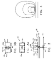
- the capacitor mounting structure generally designated as 40 for minimizing parasitic inductance is illustrated.
- the PCB board generally designated as B includes the ground plane 10 and power plane 11 and has upper surface 10a.
- Three vias 41, 42 and 43, are positioned in substantially straight line alignment as illustrated in Fig. 3B and are located substantially adjacent to each other in a row, which row is approximately aligned with the centerline 50 of the capacitor 15.
- the vias 41-43 alternately electrically connect to either ground plane 10 or voltage plane 11.
- tubular section of via 43 is electrically connected to the voltage plane 11 and extends through an opening in the ground plane 10.
- the tubular section of via 42 is electrically connected to the ground plane 10 and extends through an opening in the power plane 11.
- via 41 is electrically connected to the power plane 11.
- the conductor pad or footprint 44 for via 42 is generally T-shaped and includes a central rectangular portion 44a formed with an extension or finger portion 44b, which extends into attachment to the top of the via 42.
- the conductor pad 45 for vias 41 and 43 is generally U-shaped.
- a central rectangular portion 45a includes first and second extensions or fingers 45b and 45c which extend into connection with vias 41 and 43.
- a U-shaped recess is formed between the conductor pad extensions 45b and 45c.
- the conductor pad U-shaped recess formed between conductor pad extensions 45b and 45c receives the extension 44b for conductor pad 44. In this manner, the conductor pad extensions are interdigitated with respect to each other, so that effective electrical connection can be made with the vias 41-43 in substantially a straight line.
- the capacitor end metal caps 15a and 15b are soldered onto the rectangular portions 45a and 44a of the pads, respectively.
- the solder pads 47 and 48 are applied as thinly as possible, such that there is little separation or thickness d'' between the capacitor bottom surface and the conductor pads.
- the cross-sectional area I'' between the conductor pads, the solder points 47 and 48 and the bottom of the central capacitor section 15C is minimized in area, thereby minimizing the distance d'' between the bottom of the capacitor and the pads 44 and 45 wherein parasitic inductor can be generated.
- Reduction of the distance d'' between the conductor pads 44 and 45 and the bottom of the capacitor 15 maximizes the aspect ratio and minimizes the generation of inductance by maximizing reluctance. It is noted that placement of the conductor pads under the central section of the capacitor 15 also acts to reduce thickness d''.
- Fig. 4 the effect of the constriction on parasitic inductance generating region is illustrated. Constricting the field lines increases the reluctance of the magnetic path which in turn reduces magnetic flux and thus reduces inductance.
- interdigitated vias formed by pad extensions 45b and c and 44b form a low inductance structure. It is believed that the insertion of the via 42 between vias 41 and 43 reduces inductance by a factor approaching 50%. A designer might typically add a pair of opposing vias (connected to ground and voltage planes) to reduce inductance roughly 50%; however, the proposed structure of Fig. 3 achieves the same benefit with only 3 vias instead of 4.
- any number of vias could be added in a line, such that current would be returned under the capacitor in a position complementary to the current flowing through the capacitor, which minimizes parasitic inductance. It is contemplated that more vias may be utilized as smaller geometries become feasible.
Landscapes
- Engineering & Computer Science (AREA)
- Microelectronics & Electronic Packaging (AREA)
- Physics & Mathematics (AREA)
- Electromagnetism (AREA)
- Manufacturing & Machinery (AREA)
- Structures For Mounting Electric Components On Printed Circuit Boards (AREA)
- Combinations Of Printed Boards (AREA)
Applications Claiming Priority (2)
| Application Number | Priority Date | Filing Date | Title |
|---|---|---|---|
| US35393 | 1993-03-22 | ||
| US08/035,393 US5375035A (en) | 1993-03-22 | 1993-03-22 | Capacitor mounting structure for printed circuit boards |
Publications (2)
| Publication Number | Publication Date |
|---|---|
| EP0617568A1 true EP0617568A1 (fr) | 1994-09-28 |
| EP0617568B1 EP0617568B1 (fr) | 1997-07-02 |
Family
ID=21882407
Family Applications (1)
| Application Number | Title | Priority Date | Filing Date |
|---|---|---|---|
| EP94301987A Expired - Lifetime EP0617568B1 (fr) | 1993-03-22 | 1994-03-21 | Structure de montage de condensateur pour circuits imprimés |
Country Status (7)
| Country | Link |
|---|---|
| US (2) | US5375035A (fr) |
| EP (1) | EP0617568B1 (fr) |
| JP (1) | JPH076928A (fr) |
| AT (1) | ATE155000T1 (fr) |
| CA (1) | CA2117239C (fr) |
| DE (1) | DE69403981T2 (fr) |
| SG (1) | SG52639A1 (fr) |
Cited By (2)
| Publication number | Priority date | Publication date | Assignee | Title |
|---|---|---|---|---|
| GB2313961A (en) * | 1996-06-08 | 1997-12-10 | Motorola Inc | Preventing dislocation of surface mounted components during soldering |
| EP1111969A1 (fr) * | 1999-12-21 | 2001-06-27 | International Business Machines Corporation | Procédé et structure pour réduire le bruit de puissance |
Families Citing this family (25)
| Publication number | Priority date | Publication date | Assignee | Title |
|---|---|---|---|---|
| US5375035A (en) * | 1993-03-22 | 1994-12-20 | Compaq Computer Corporation | Capacitor mounting structure for printed circuit boards |
| US5761049A (en) * | 1994-09-19 | 1998-06-02 | Hitachi, Ltd. | Inductance cancelled condenser implemented apparatus |
| US5661420A (en) * | 1995-03-08 | 1997-08-26 | Etymotic Research, Inc. | Mounting configuration for monolithic integrated circuit |
| JP3581971B2 (ja) * | 1996-05-22 | 2004-10-27 | 株式会社ボッシュオートモーティブシステム | 車載用コントロールユニットのemi用接地構造 |
| US5731960A (en) * | 1996-09-19 | 1998-03-24 | Bay Networks, Inc. | Low inductance decoupling capacitor arrangement |
| US6020562A (en) * | 1997-11-11 | 2000-02-01 | 3Com Corporation | Reduced-capacitance component mounting pads and capacitance-reduction methods for high frequency multi-layer printed circuit boards |
| US6252177B1 (en) | 1998-02-18 | 2001-06-26 | Compaq Computer Corporation | Low inductance capacitor mounting structure for capacitors of a printed circuit board |
| US6456502B1 (en) * | 1998-09-21 | 2002-09-24 | Compaq Computer Corporation | Integrated circuit device/circuit board connection apparatus |
| JP3822390B2 (ja) * | 1998-09-30 | 2006-09-20 | 太陽誘電株式会社 | 混成集積回路装置 |
| EP1075004A4 (fr) * | 1999-02-17 | 2007-05-02 | Tdk Corp | Condensateur |
| US6356429B2 (en) * | 1999-02-18 | 2002-03-12 | Tdk Corporation | Capacitor |
| US6525921B1 (en) * | 1999-11-12 | 2003-02-25 | Matsushita Electric Industrial Co., Ltd | Capacitor-mounted metal foil and a method for producing the same, and a circuit board and a method for producing the same |
| US6617526B2 (en) * | 2001-04-23 | 2003-09-09 | Lockheed Martin Corporation | UHF ground interconnects |
| US7312402B2 (en) * | 2002-10-11 | 2007-12-25 | International Business Machines Corporation | Method and apparatus for providing improved loop inductance of decoupling capacitors |
| US7645940B2 (en) * | 2004-02-06 | 2010-01-12 | Solectron Corporation | Substrate with via and pad structures |
| DE102005017527A1 (de) * | 2005-04-15 | 2006-11-02 | Osram Opto Semiconductors Gmbh | Oberflächenmontierbares optoelektronisches Bauelement |
| CN1889808A (zh) * | 2005-06-28 | 2007-01-03 | 鸿富锦精密工业(深圳)有限公司 | 印刷电路板重叠焊盘的布线结构 |
| US7746660B1 (en) * | 2006-10-10 | 2010-06-29 | Xilinx, Inc. | Reduced mounting inductance and increased self-resonant frequency range |
| DE202008005708U1 (de) * | 2008-04-24 | 2008-07-10 | Vishay Semiconductor Gmbh | Oberflächenmontierbares elektronisches Bauelement |
| JP5339092B2 (ja) * | 2010-07-22 | 2013-11-13 | Tdk株式会社 | バンドパスフィルタモジュール及びモジュール基板 |
| JP5655818B2 (ja) | 2012-06-12 | 2015-01-21 | 株式会社村田製作所 | チップ部品構造体 |
| JP6014581B2 (ja) * | 2013-02-18 | 2016-10-25 | 太陽誘電株式会社 | インターポーザ付き積層セラミックコンデンサと、積層セラミックコンデンサ用インターポーザ |
| US9831035B2 (en) | 2014-10-31 | 2017-11-28 | Deere & Company | Capacitor with improved heat dissipation |
| US9439278B2 (en) | 2014-12-12 | 2016-09-06 | Deere & Company | Film capacitor having a package for heat transfer |
| KR102849159B1 (ko) | 2020-10-27 | 2025-08-25 | 삼성전자주식회사 | 반도체 패키지 |
Citations (1)
| Publication number | Priority date | Publication date | Assignee | Title |
|---|---|---|---|---|
| JPH04211191A (ja) * | 1990-02-09 | 1992-08-03 | Hitachi Ltd | 実装構造体 |
Family Cites Families (15)
| Publication number | Priority date | Publication date | Assignee | Title |
|---|---|---|---|---|
| US3302067A (en) * | 1967-01-31 | Modular circuit package utilizing solder coated | ||
| US3403438A (en) * | 1964-12-02 | 1968-10-01 | Corning Glass Works | Process for joining transistor chip to printed circuit |
| US3967296A (en) * | 1972-10-12 | 1976-06-29 | General Electric Company | Semiconductor devices |
| US3934073A (en) * | 1973-09-05 | 1976-01-20 | F Ardezzone | Miniature circuit connection and packaging techniques |
| US4130722A (en) * | 1977-01-10 | 1978-12-19 | Globe-Union Inc. | Thick-film circuit module including a monolithic ceramic cross-over device |
| US4430690A (en) * | 1982-10-07 | 1984-02-07 | International Business Machines Corporation | Low inductance MLC capacitor with metal impregnation and solder bar contact |
| US4754366A (en) * | 1985-01-22 | 1988-06-28 | Rogers Corporation | Decoupling capacitor for leadless surface mounted chip carrier |
| US4648006A (en) * | 1985-03-26 | 1987-03-03 | Illinois Tool Works Inc. | Plastic chip capacitor for surface mounting |
| JPH01198091A (ja) * | 1988-02-02 | 1989-08-09 | Mitsubishi Electric Corp | 混成集積回路基板 |
| US4910643A (en) * | 1988-06-06 | 1990-03-20 | General Electric Company | Thick film, multi-layer, ceramic interconnected circuit board |
| US4954929A (en) * | 1989-08-22 | 1990-09-04 | Ast Research, Inc. | Multi-layer circuit board that suppresses radio frequency interference from high frequency signals |
| JP2796682B2 (ja) * | 1990-01-12 | 1998-09-10 | 山九株式会社 | 錨型自動玉外しフック装置 |
| JPH04367212A (ja) * | 1991-06-14 | 1992-12-18 | Nec Corp | チップ型固体電解コンデンサの製造方法 |
| US5210683A (en) * | 1991-08-22 | 1993-05-11 | Lsi Logic Corporation | Recessed chip capacitor wells with cleaning channels on integrated circuit packages |
| US5375035A (en) * | 1993-03-22 | 1994-12-20 | Compaq Computer Corporation | Capacitor mounting structure for printed circuit boards |
-
1993
- 1993-03-22 US US08/035,393 patent/US5375035A/en not_active Expired - Lifetime
-
1994
- 1994-03-08 CA CA002117239A patent/CA2117239C/fr not_active Expired - Fee Related
- 1994-03-21 AT AT94301987T patent/ATE155000T1/de not_active IP Right Cessation
- 1994-03-21 EP EP94301987A patent/EP0617568B1/fr not_active Expired - Lifetime
- 1994-03-21 DE DE69403981T patent/DE69403981T2/de not_active Expired - Fee Related
- 1994-03-21 SG SG1996007234A patent/SG52639A1/en unknown
- 1994-03-22 JP JP6075301A patent/JPH076928A/ja active Pending
- 1994-06-03 US US08/253,980 patent/US5459642A/en not_active Expired - Lifetime
Patent Citations (1)
| Publication number | Priority date | Publication date | Assignee | Title |
|---|---|---|---|---|
| JPH04211191A (ja) * | 1990-02-09 | 1992-08-03 | Hitachi Ltd | 実装構造体 |
Non-Patent Citations (2)
| Title |
|---|
| "decoupling capacitor placement", IBM TECHNICAL DISCLOSURE BULLETIN, vol. 19, no. 8, January 1977 (1977-01-01), US, pages 3046 - 3047 * |
| PATENT ABSTRACTS OF JAPAN vol. 16, no. 554 (E - 1293) 25 November 1992 (1992-11-25) * |
Cited By (2)
| Publication number | Priority date | Publication date | Assignee | Title |
|---|---|---|---|---|
| GB2313961A (en) * | 1996-06-08 | 1997-12-10 | Motorola Inc | Preventing dislocation of surface mounted components during soldering |
| EP1111969A1 (fr) * | 1999-12-21 | 2001-06-27 | International Business Machines Corporation | Procédé et structure pour réduire le bruit de puissance |
Also Published As
| Publication number | Publication date |
|---|---|
| SG52639A1 (en) | 1998-09-28 |
| CA2117239C (fr) | 1998-08-25 |
| EP0617568B1 (fr) | 1997-07-02 |
| DE69403981T2 (de) | 1998-01-22 |
| CA2117239A1 (fr) | 1994-09-23 |
| JPH076928A (ja) | 1995-01-10 |
| DE69403981D1 (de) | 1997-08-07 |
| US5459642A (en) | 1995-10-17 |
| ATE155000T1 (de) | 1997-07-15 |
| US5375035A (en) | 1994-12-20 |
Similar Documents
| Publication | Publication Date | Title |
|---|---|---|
| EP0617568B1 (fr) | Structure de montage de condensateur pour circuits imprimés | |
| US6983535B2 (en) | Insertion of electrical component within a via of a printed circuit board | |
| US4782311A (en) | Three terminal filter | |
| US6418009B1 (en) | Broadband multi-layer capacitor | |
| US8941459B2 (en) | Low profile inductors for high density circuit boards | |
| US20080239622A1 (en) | Wiring structure of laminated capacitors | |
| WO1999019934A1 (fr) | Dispositif de couplage pour montage en surface | |
| JP2003109822A (ja) | プリント回路ボード | |
| WO2007146580A1 (fr) | Carte de circuit imprimé à connecteurs électriques coextensifs et zones de pastilles de contact | |
| EP0311418A2 (fr) | Elément composé en forme de pastille | |
| KR100747130B1 (ko) | Bga 패키지들에 대해 향상된 바이패스 디커플링을 갖는인쇄 회로 기판 조립체 | |
| KR100727264B1 (ko) | 노이즈 필터의 실장구조 | |
| KR0145183B1 (ko) | Lc 노이즈 필터 | |
| US5761049A (en) | Inductance cancelled condenser implemented apparatus | |
| EP1349271B1 (fr) | Circuit d'alimentation en tension continue comportant un filtre antiparasite | |
| US20190180930A1 (en) | Dc-dc converter module | |
| JPH0318113A (ja) | ノイズフィルタの取付け構造 | |
| US7369018B2 (en) | Dielectric filter | |
| JP2977018B2 (ja) | インタフェースケーブル接続用コネクタ | |
| JPS62139395A (ja) | 多機能回路基板 | |
| CN100431071C (zh) | 多端子smt bga型卷绕电容器 | |
| JP2001326432A (ja) | プリント配線板とケーブルの接続構造及び電子機器 | |
| US20030103341A1 (en) | Shielding structure for resonant circuit | |
| JPH11259172A (ja) | 電子機器 | |
| JP2000244128A (ja) | 多層プリント配線基板及びそれを用いたチップ型3端子ノイズフィルタの実装構造 |
Legal Events
| Date | Code | Title | Description |
|---|---|---|---|
| PUAI | Public reference made under article 153(3) epc to a published international application that has entered the european phase |
Free format text: ORIGINAL CODE: 0009012 |
|
| AK | Designated contracting states |
Kind code of ref document: A1 Designated state(s): AT BE CH DE DK ES FR GB IE IT LI NL SE |
|
| 17P | Request for examination filed |
Effective date: 19950324 |
|
| 17Q | First examination report despatched |
Effective date: 19950927 |
|
| GRAG | Despatch of communication of intention to grant |
Free format text: ORIGINAL CODE: EPIDOS AGRA |
|
| GRAG | Despatch of communication of intention to grant |
Free format text: ORIGINAL CODE: EPIDOS AGRA |
|
| GRAH | Despatch of communication of intention to grant a patent |
Free format text: ORIGINAL CODE: EPIDOS IGRA |
|
| GRAH | Despatch of communication of intention to grant a patent |
Free format text: ORIGINAL CODE: EPIDOS IGRA |
|
| GRAA | (expected) grant |
Free format text: ORIGINAL CODE: 0009210 |
|
| AK | Designated contracting states |
Kind code of ref document: B1 Designated state(s): AT BE CH DE DK ES FR GB IE IT LI NL SE |
|
| PG25 | Lapsed in a contracting state [announced via postgrant information from national office to epo] |
Ref country code: NL Free format text: LAPSE BECAUSE OF FAILURE TO SUBMIT A TRANSLATION OF THE DESCRIPTION OR TO PAY THE FEE WITHIN THE PRESCRIBED TIME-LIMIT Effective date: 19970702 Ref country code: LI Effective date: 19970702 Ref country code: IT Free format text: LAPSE BECAUSE OF FAILURE TO SUBMIT A TRANSLATION OF THE DESCRIPTION OR TO PAY THE FEE WITHIN THE PRESCRIBED TIME-LIMIT;WARNING: LAPSES OF ITALIAN PATENTS WITH EFFECTIVE DATE BEFORE 2007 MAY HAVE OCCURRED AT ANY TIME BEFORE 2007. THE CORRECT EFFECTIVE DATE MAY BE DIFFERENT FROM THE ONE RECORDED. Effective date: 19970702 Ref country code: ES Free format text: THE PATENT HAS BEEN ANNULLED BY A DECISION OF A NATIONAL AUTHORITY Effective date: 19970702 Ref country code: DK Effective date: 19970702 Ref country code: CH Effective date: 19970702 Ref country code: BE Effective date: 19970702 Ref country code: AT Effective date: 19970702 |
|
| REF | Corresponds to: |
Ref document number: 155000 Country of ref document: AT Date of ref document: 19970715 Kind code of ref document: T |
|
| REG | Reference to a national code |
Ref country code: CH Ref legal event code: EP |
|
| REF | Corresponds to: |
Ref document number: 69403981 Country of ref document: DE Date of ref document: 19970807 |
|
| PG25 | Lapsed in a contracting state [announced via postgrant information from national office to epo] |
Ref country code: SE Effective date: 19971002 |
|
| ET | Fr: translation filed | ||
| NLV1 | Nl: lapsed or annulled due to failure to fulfill the requirements of art. 29p and 29m of the patents act | ||
| REG | Reference to a national code |
Ref country code: CH Ref legal event code: PL |
|
| PG25 | Lapsed in a contracting state [announced via postgrant information from national office to epo] |
Ref country code: IE Free format text: LAPSE BECAUSE OF NON-PAYMENT OF DUE FEES Effective date: 19980321 |
|
| PLBE | No opposition filed within time limit |
Free format text: ORIGINAL CODE: 0009261 |
|
| STAA | Information on the status of an ep patent application or granted ep patent |
Free format text: STATUS: NO OPPOSITION FILED WITHIN TIME LIMIT |
|
| 26N | No opposition filed | ||
| REG | Reference to a national code |
Ref country code: GB Ref legal event code: IF02 |
|
| PGFP | Annual fee paid to national office [announced via postgrant information from national office to epo] |
Ref country code: DE Payment date: 20080430 Year of fee payment: 15 |
|
| PG25 | Lapsed in a contracting state [announced via postgrant information from national office to epo] |
Ref country code: DE Free format text: LAPSE BECAUSE OF NON-PAYMENT OF DUE FEES Effective date: 20091001 |
|
| REG | Reference to a national code |
Ref country code: GB Ref legal event code: 732E Free format text: REGISTERED BETWEEN 20120412 AND 20120418 |
|
| PGFP | Annual fee paid to national office [announced via postgrant information from national office to epo] |
Ref country code: GB Payment date: 20130228 Year of fee payment: 20 |
|
| PGFP | Annual fee paid to national office [announced via postgrant information from national office to epo] |
Ref country code: FR Payment date: 20130429 Year of fee payment: 20 |
|
| REG | Reference to a national code |
Ref country code: FR Ref legal event code: TP Owner name: HEWLETT-PACKARD DEVELOPMENT COMPANY, L.P., US Effective date: 20131018 |
|
| REG | Reference to a national code |
Ref country code: GB Ref legal event code: PE20 Expiry date: 20140320 |
|
| PG25 | Lapsed in a contracting state [announced via postgrant information from national office to epo] |
Ref country code: GB Free format text: LAPSE BECAUSE OF EXPIRATION OF PROTECTION Effective date: 20140320 |