EP0617573A1 - Système de drainage de vapeur - Google Patents
Système de drainage de vapeur Download PDFInfo
- Publication number
- EP0617573A1 EP0617573A1 EP94102707A EP94102707A EP0617573A1 EP 0617573 A1 EP0617573 A1 EP 0617573A1 EP 94102707 A EP94102707 A EP 94102707A EP 94102707 A EP94102707 A EP 94102707A EP 0617573 A1 EP0617573 A1 EP 0617573A1
- Authority
- EP
- European Patent Office
- Prior art keywords
- vapor
- enclosure
- removal element
- drain system
- vapor removal
- Prior art date
- Legal status (The legal status is an assumption and is not a legal conclusion. Google has not performed a legal analysis and makes no representation as to the accuracy of the status listed.)
- Granted
Links
Images






Classifications
-
- H—ELECTRICITY
- H10—SEMICONDUCTOR DEVICES; ELECTRIC SOLID-STATE DEVICES NOT OTHERWISE PROVIDED FOR
- H10P—GENERIC PROCESSES OR APPARATUS FOR THE MANUFACTURE OR TREATMENT OF DEVICES COVERED BY CLASS H10
- H10P72/00—Handling or holding of wafers, substrates or devices during manufacture or treatment thereof
- H10P72/10—Handling or holding of wafers, substrates or devices during manufacture or treatment thereof using carriers specially adapted therefor, e.g. front opening unified pods [FOUP]
- H10P72/19—Handling or holding of wafers, substrates or devices during manufacture or treatment thereof using carriers specially adapted therefor, e.g. front opening unified pods [FOUP] closed carriers
- H10P72/1911—Handling or holding of wafers, substrates or devices during manufacture or treatment thereof using carriers specially adapted therefor, e.g. front opening unified pods [FOUP] closed carriers characterised by materials, roughness, coatings or the like
-
- B—PERFORMING OPERATIONS; TRANSPORTING
- B65—CONVEYING; PACKING; STORING; HANDLING THIN OR FILAMENTARY MATERIAL
- B65G—TRANSPORT OR STORAGE DEVICES, e.g. CONVEYORS FOR LOADING OR TIPPING, SHOP CONVEYOR SYSTEMS OR PNEUMATIC TUBE CONVEYORS
- B65G1/00—Storing articles, individually or in orderly arrangement, in warehouses or magazines
-
- H—ELECTRICITY
- H10—SEMICONDUCTOR DEVICES; ELECTRIC SOLID-STATE DEVICES NOT OTHERWISE PROVIDED FOR
- H10P—GENERIC PROCESSES OR APPARATUS FOR THE MANUFACTURE OR TREATMENT OF DEVICES COVERED BY CLASS H10
- H10P72/00—Handling or holding of wafers, substrates or devices during manufacture or treatment thereof
- H10P72/10—Handling or holding of wafers, substrates or devices during manufacture or treatment thereof using carriers specially adapted therefor, e.g. front opening unified pods [FOUP]
- H10P72/19—Handling or holding of wafers, substrates or devices during manufacture or treatment thereof using carriers specially adapted therefor, e.g. front opening unified pods [FOUP] closed carriers
- H10P72/1924—Handling or holding of wafers, substrates or devices during manufacture or treatment thereof using carriers specially adapted therefor, e.g. front opening unified pods [FOUP] closed carriers characterised by atmosphere control
- H10P72/1926—Handling or holding of wafers, substrates or devices during manufacture or treatment thereof using carriers specially adapted therefor, e.g. front opening unified pods [FOUP] closed carriers characterised by atmosphere control characterised by the presence of atmosphere modifying elements inside or attached to the closed carrier
Definitions
- the present invention relates to transportable enclosures for reducing particle contamination during manufacture, storage or transportation of components and more particularly to standardized mechanical interface (SMIF) systems employing a vapor drain system for removing chemical vapors and components from within the enclosure.
- SMIF standardized mechanical interface
- Chemical vapor contaminants are known to alter the processes used to manufacture sensitive devices such as micro-circuitry. Such chemical vapor contaminants have historically been inadequately addressed. These vapor contaminants originate from a variety of sources, including the enclosures used to protect components from particulate contamination. Outgassing of plastics, adhesives and sealant materials can make the enclosure itself a source of chemical contaminants. In addition, externally produced vapors are capable of contaminating an open enclosure. Later, when the enclosure contains a sensitive component, such as a semiconductor wafer, these vapors can be reemitted and contaminate the wafer.
- Chemical contamination is beginning to be recognized as a major factor in manufacturing operations. Such contamination was first recognized in process chemicals, such as impurities in gases used in semiconductor device manufacture and in solvent residues.
- Process contamination caused by environmental air-borne vapors is also a growing problem. Such vapors are everywhere in the environment at low concentrations.
- the origin of the vapor is diverse and includes plasticizer vapors, process materials from elsewhere in a factory, chemicals used in cleaning and air conditioning systems, cosmetics, adhesives and chemicals used in neighboring factories and in agriculture. These contaminants can degrade manufacturing by affecting the sensitivity of lithographic, etch and other processes, interfering with adhesion between surfaces, altering the wetability of surfaces, reducing effectiveness of cleaning processes, interfering with chemical reactions and inducing corrosion of metallurgy.
- Some chemical compounds are capable of travelling as vapors which deposit a mono-molecular layer on the wafer, which degrades subsequent wafer manufacturing processes and product quality.
- An important class of organic compounds has a molecular mass between approximately 150 and 600 AMU (atomic mass units) and non-specific chemical reactivity. These compounds emit significant vapors and adhere as a mono-molecular layer to cause product degradation.
- One such compound is dialkyl-phthalate, which is a widely used plasticizer.
- organic compounds having much larger molecular masses typically do not emit significant vapor and organic compounds having much smaller molecular mass typically do not adhere sufficiently to a surface, and hence both types of components usually do not pose a problem.
- halogenated solvents e.g., di-chloro-methane or tri-chloro-ethane
- organic acids e.g., acrylic or benzoic acids
- Vapor self-contamination is particularly relevant. Even a sealed enclosure traps and accumulates vapors. The vapors are emitted by enclosure materials (such as plastics, adhesives, sealants and their trace components), external vapors absorbed onto the enclosure surfaces and into seals when the enclosure is open, and vapors emitted by nascent products.
- enclosure materials such as plastics, adhesives, sealants and their trace components
- Process chemicals and enclosure materials should be chemically selected to minimize these problems. In view of practical restraints, it is very difficult to eliminate contamination from trace vapors and mono-molecular layers solely by material selection. Moreover, vapor emission is only one of the criteria which must be met by nascent process materials such as resists.
- SMIF standardized mechanical interface
- the present invention overcomes the difficulties encountered by heretofore known enclosures by equipping each enclosure or SMIF system with a device which acts to remove vapors and shall be referred to hereinafter as a vapor removal element. While the invention is primarily intended for use in connection with a SMIF system, the invention is equally applicable for use with any sealed enclosure used for manufacturing, storing or transporting of components sensitive to chemical vapors.
- the present invention has application to any product with potential or known sensitivity to vapor borne contamination, such as pharmaceuticals, clinical diagnostic and therapeutic products, chemicals and genetically engineered products.
- the present invention teaches the use of a vapor drain system to counteract vapor contamination, particularly from sources which emit vapors inside the enclosure.
- vapor emission by the source is counterbalanced by vapor removal by the vapor drain system.
- a steady state condition will result with a small or otherwise acceptable vapor concentration in the environment within the enclosure.
- the former is provided preferably by vapor diffusion between a wafer and a closely spaced vapor drain or by air movement and vapor convection between a wafer and more distantly disposed vapor drain.
- a vapor drain system typically comprises two structures: a global/aero structure and a vapor removal element which brings together vapors and the vapor removal element.
- the internal structure of the vapor removal element removes vapor from the surrounding environment.
- a typical vapor removal element or internal structure includes an absorber layer for absorbing vapors (e.g. activated carbon cloth), a barrier layer for separating the absorber from a particulate-sensitive region (e.g. HEPA (high efficiency particular air) filter or permeable organic membrane) and a guard plate, usually with channels to guide air and stiffness for mechanical support and protection.
- absorber layer for absorbing vapors
- barrier layer for separating the absorber from a particulate-sensitive region (e.g. HEPA (high efficiency particular air) filter or permeable organic membrane)
- a guard plate usually with channels to guide air and stiffness for mechanical support and protection.
- these structures are thin and are congruent with a wafer.
- inventions include an internal structure comprising a vapor-absorbing coating on a substrate.
- the coating is preferably titanium, deposited carbon or oxidized/activated resist or other organic polymer.
- Selection of a preferred embodiment for the global/aero structure depends upon the enclosure structure, the vapor sources (including intensity and location), the vapor chemistry and wafer surface. The selection is also dependent upon the enclosure usage, i.e. cost and machine, procedure, policy for loading/unloading wafers in the enclosure and enclosure cleaning.
- An especially simple global/aero embodiment protects a single wafer enclosure by locating the vapor-sensitive surface of the wafer closely adjacent to a thin vapor removal element in the base of the enclosure.
- a global vapor drain system comprises a large thin vapor removal element inside the enclosure cover.
- This embodiment is simple to implement, compatible with existing equipment and processing procedures and can counteract moderate vapor sources.
- a closely adjacent vapor drain system arrangement is used where each wafer is disposed closely adjacent to an individual vapor removal element. When loading/unloading the enclosure, each wafer and its associated vapor removal element are handled as a single unit. This embodiment counteracts very intense vapor sources, but complicates load/unload procedures.
- vapor removal elements and wafers are alternated throughout the stack.
- This embodiment counter-acts intermediate vapor sources, complicates load/unload procedures and reduces enclosure capacity by 50 percent.
- a flip-leaved vapor drain system arrangement is employed where a two-sided vapor removal element is disposed between pairs of wafers in a stack. This embodiment provides intermediate vapor removal, complicates load/unload procedures, but reduces enclosure capacity by only one-third.
- an integrated sheet vapor drain system arrangement is employed when the back of each wafer is coated with an absorbing layer for removing vapors from the surface of the adjoining wafer. This embodiment maximizes enclosure capacity, facilitates existing load/unload procedures but require the addition of a special coating on each wafer.
- a vapor removal element is located inside the cover of the enclosure.
- the air within the enclosure is heated near the bottom and cooled near the top of the enclosure.
- the non-uniform temperature difference in the air produces a non-uniform air density, buoyant forces and air circulation.
- the result is that vapors are carried close to the vapor removal element for improved vapor removal.
- This embodiment can counteract even strong vapor sources with undiminished wafer capacity per enclosure, but requires a more complex enclosure design.
- a vapor removal element is located in the cover, usually on a sidewall. Inside of the enclosure are a fan and an optional particulate filter.
- the fan forces air circulation which convects any vapor past the vapor removal element for improved vapor removal.
- This design counter-acts intense contamination, facilitates conventional load/unload procedures and maximizes enclosure capacity but adds appreciably to the complexity of the enclosure.
- an air blower and air duct are provided.
- a porous vapor removal element and particulate filter are disposed across the duct opening for trapping vapors which the fan forces into the duct. This embodiment provides aggressive vapor removal and permits existing load/unload procedures with maximum enclosure capacity at the cost of significantly increased enclosure complexity.
- a breather vapor drain system is located across an aperture in the cover of the enclosure. During barometric and thermal cycles, the enclosure breathes through the vapor removal element and exchanges inside and outside air. The breather vapor drain prevents external vapors from entering the enclosure and also counteracts moderate internal vapor sources.
- porous vapor removal elements are located across both of two apertures on opposite sidewalls of the enclosure cover. Air is forced into the enclosure through one vapor removal element and removed from the enclosure through the other vapor removal element. This embodiment counteracts external vapors, moderate internal vapor sources but requires external air connections.
- Another embodiment is a sampler vapor drain system where the vapor removal element collects a sample of the vapor for analysis.
- a vapor removal element which reversibly absorbs vapors.
- a reservoir vapor drain system which includes a reservoir containing a chemical which emits a desirable vapor such as an anti-corrosion agent or an anti-electro-static agent.
- the resulting enclosure must be compatible with existing enclosures in terms of function, related tools and techniques.
- the vapor drain system should be particulate-free, compatible with a sealed enclosure which blocks particulate, compatible with loading and unloading wafers in the enclosure, compatible with wafer processing and enclosure cleaning methods.
- the various embodiments of this invention provide compatibility with various classes of enclosures: enclosures for a single wafer or multiple wafers, an enclosure for use with stagnant air or moving air, an enclosure which permits or does not permit a vapor removal element to be mounted like a wafer, and particularly compatible with various SMIF enclosures.
- the vapor removal element may be in the form of a chemical absorber, e.g. activated carbon placed inside a micro-porous membrane to prevent dust emissions.
- the absorber causes vapor removal from the environment which counterbalances vapor emission. Proper vapor engineering results in a steady state condition and very low vapor concentration.
- absorber will be understood to include vapor removal by adsorption, absorption, physisorption, chemisorption, bulk chemical reaction, and even permeation through a membrane to a sink for vapor.
- air will be understood to include not only normal air, but any other gas, such as dry nitrogen.
- wafer will be understood to include not only semiconductor wafers but also dense printed circuits, display panels, disks or plates for information storage (including storage by magnetic, optical, magneto-optical, and scanning tunneling microscope processes) or other components.
- wafer will be understood to include various biological, pharmaceutical and bio-engineered products.
- nascent wafer will be understood to mean a wafer in the course of fabrication, particularly when it is vulnerable to chemical vapor.
- enclosure will be understood to include not only SMIF pods or SMIF enclosures, and wafer boxes, but also so-called “orange boxes” for multiple wafers, and “single wafer boxes” and various cassettes. More generally “enclosure” will be understood to include any substantially closed structure to separate nascent wafers from the external environment during fabrication, manufacturing, processing, storage, transfer, or shipment.
- One contamination source is the enclosure material itself.
- gaskets often use silicon rubber which can emit silicone oil and degrade adhesion during subsequent wafer fabrication.
- other enclosure materials such as plastics, adhesives, sealants and their trace components
- emit vapors often emit vapors.
- Another source of contamination is indirect contamination of the enclosure.
- external vapors can contaminate the enclosure surfaces and seals. Later, when the enclosure contains nascent wafers, these vapors can be re-emitted and contaminate enclosed wafers.
- the nascent wafer itself is another source of contamination which carries and emits process chemicals. These chemicals can contaminate enclosure surfaces. Later these surfaces can emit the chemicals as vapors and contaminate the wafers at later processing stages, where the same chemicals then cause damage.
- an enclosure including a suitable vapor drain system By using an enclosure including a suitable vapor drain system the chemical vapor contamination can be prevented, even in a closed enclosure. However, it may be more reliable to prevent particulate contamination in a closed enclosure than to prevent it in a well-ventilated open clean room. Moreover, an enclosure allows production of high density wafers in an existing clean room, without very expensive clean room upgrades.
- a vapor drain system removes vapors emitted inside of the enclosure, and/or prevents entry of vapors from outside the enclosure.
- the vapor conductance or normalized vapor removal rate from a wafer to a vapor drain is determined by the geometry and aerodynamics of the enclosure and the vapor drain system using vapor diffusion, vapor buoyant convection, or vapor forced convection.
- a principal object of the present invention is therefore, the provision of an enclosure including a vapor drain system for minimizing chemical vapor contamination of a component in the enclosure.
- Another object of the invention is the provision of an enclosure including a vapor drain system for removing vapors from within the enclosure.
- a further object of the invention is the provision of an enclosure including a vapor drain system for lowering the vapor concentration within the enclosure from vapor sources located within the enclosure.
- a still further object of the invention is the provision of an enclosure including a vapor drain system which is compatible with existing enclosures and related tools and processing methods.
- the enclosure 10 is a flat cylindrical box, slightly larger than a wafer 12.
- the enclosure includes a shallow base 24, a cover 20, a sealing mechanism presses from the cover 20, to the perimeter region 16 of the wafer 12 adjacent to the concave base 24.
- the spring maintains the position of wafer 12, and prevents contact with the sensitive face 14.
- the base 24, cover 20, and spring 22 are made of particulate-free material, typically high density polyethylene.
- Fig. 2 shows a more typical enclosure 40 which is designed to hold many wafers 12 during fabrication. Such a design is described in U.S. Patent No. 4,739,882, and is of the type manufactured by Asyst Inc.
- the enclosure includes a rigid base 42, a box-like cover 44, and a gasket 46 to exclude external air and particulates. Inside the enclosure there is a frame 48, with brackets 52. Each wafer 12 spans a pair of brackets 52 at a respective site 50 in a stack 18 of wafers 12. Each wafer 12 has a sensitive face 14.
- a representative SMIF pod can enclose 25 wafers, each 200 mm diameter, and has external dimensions approximately 40 cm wide, 40 cm deep, and 50 cm tall.
- the stack 18 of wafers 12 has a pitch of approximately 8 mm.
- a preferred vapor drain system includes a vapor removal element and a global/aero structure.
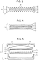
- Fig. 3 shows the vapor removal element of a preferred embodiment of a vapor removal element 30.
- a blown-up cross section with considerable exaggeration of vertical thicknesses and clearances.
- the vapor removal element 30 comprises several stacked layers of vapor removal elements. At the center of the vapor removal element 30 is an absorber layer 32.
- a preferred absorber material is activated carbon fabric, such as Kynol® ACC material produced by Nippon-Kynol Inc.
- Surrounding absorber layer 32 is a barrier layer 34 which is permeable to vapor, but blocks particulates.
- a preferred barrier layer is a micro-porous membrance of expanded permeable PTFE (Poly-Tetra-Fluoro-Ethylene).
- An alternative preferred barrier layer is a laminated micro-fiber filter, such as used in a typical HEPA filter material.
- barrier layer is an electro-statically charged web, such as ElecTreet® by Donaldson Inc.
- the barrier layer typically has a polyester scrim bonded with fusable polyethene web.
- the bottom and top parts of the barrier layer 34 completely enclose the absorber layer 32.
- Above and below the barrier layer 34 are optional guard plates 36, each relatively rigid, and each with channels 38 for allowing the passage of air.
- On each side of the vapor removal element is an internal spacer 26 or housing, and an optional external spacer 28. In some cases, these spacers may be joined with each other or with adjacent hardware.
- Any vapor located near the vapor removal element 30 will rapidly travel a small distance by diffusion, percolation or airflow, through channels 38 in guard plate 36, through a barrier layer 34, into the absorber layer 32 where the vapor is removed from the air.
- the rigid guard plates 36 mechanically protect the absorber 32. Also spacers 26 and 28 minimize mechanical forces on the guard plates 36, barrier layers 34, and absorber layer 32. The guard plate minimize crumbling and particulate formation in the absorber layer 32. Furthermore, any particulate formed in the absorber layer 32 will be trapped inside the barrier layer 34. Thus the absorber layer 32 in the vapor removal element system 30 will not emit dust.
- the preferred material for the absorber layer 32 depends on the vapor chemistry. Activated carbon fabric is preferred for organic vapors with medium molecular weight, such as di-octyl-phthalyate or silicone oil. For corrosive vapors, a better absorber material is activated carbon treated with a base. An example is neutralization and removal of benzoic acid vapor by sodium carbonate base. Another preferred material is described in U.S. Patent 5,124,856, entitled "Unitary Filter Media" and assigned to the same assignee as the present invention. Other absorber layers can include nano-porous materials such as zeolites and aero-gels. In an alternative absorber embodiment a stiff plate with holes includes a suitable resin coating, such as Novolac. The coating is polymerized to plastic and then converted in situ to activated carbon.
- vapor removal element shown in Figure 3 is used with various global/aero embodiments as described below.
- vapor is absorbed from both the top and bottom surfaces of the vapor removal element cover.
- only one side of the cover is used to absorb vapors and the other side of the vapor removal element cover may be simplified, eliminated or unified.
- the air channels 38 in guard plates 36 are designed to spread air approximately uniformly across the barrier layer 34 and absorber layer 32. This uniformity minimizes local saturation and local failure.
- the absorber layer 32 and barrier layer 34 are pleated. Pleating increases the flow area, which allows more air flow with less pressure, within a moderate volume for the vapor drain. Also, pleating increases the vapor capacity (the maximum mass of vapor which the absorber layer can hold) within a moderate volume.
- FIG. 4 shows another preferred embodiment for the internal structure, referred to as a sheet vapor removal element 54.
- the sheet vapor removal element 54 comprises several layers: substrate layer 56, an optional joining layer 58, absorber layer 60, which is preferably applied as a coating, and an optional barrier layer 62 to block dust.
- a preferred embodiment of the sheet vapor removal element includes a thin sheet of titanium which implicitly unifies several layers. However, it may be necessary to re-activate the surface, by cleaning with ultra-violet light and/or microwave radiation and/or by exposure to ozone, or by sputtering more titanium.
- the absorber layer 60 is a coating such as sputtered titanium.
- Some deposited or sputtered coatings can be quite dust-free and tough in which case, the barrier layer 62 is not needed.
- An alternative absorber layer 60 is a coating of activated carbon. In other applications, it is possible to start by applying resist or other organic coating upon the substrate 56 and then oxidize and/or activate the resist or coating in place.
- a substrate 56 is coated with an organic film and an adhesive layer 58. Then the organic film is oxidized and/or activated in place, to form an absorber layer 60 of activated carbon.
- the substrate 56 can be a sheet of stainless steel, glass, silicon or the like.
- the substrate 56 can be unified with various convenient structures, such as the inside of the cover 44 in Figure 2.
- a sheet vapor removal element 54 is formed by a coating applied inside the cover 44, the cover can be recoated as frequently as required.
- the vapor removal element has physically independent layers.
- the substrate 56 is a sheet of silicon
- the adhesive layer 58 is a discrete film layer
- the absorber layer 60 is a sheet of thin solid activated carbon
- the barrier layer 62 is a nano-porous membrane.
- FIG. 5 shows the relationship between the vapor removal element and wafer in accordance with the teachings of the present invention.
- a single wafer 12 having a sensitive face 14 is contained within an enclosure 66.
- a thin planar vapor removal element 68 such as that described above in conjunction with Figure 3, is disposed opposite the sensitive face 14 of wafer 12.
- the vapor removal element 68 covers most of the area inside the base 70.
- the base 70 is dimensioned to accommodate both the vapor removal element 68 and the wafer 12.
- a spring 22, spacers 72, 74 and a guard plate 36 hold the wafer 12 in place.
- the shallow enclosure 66 contains a wafer 12
- the vapor removal element 68 is disposed closely adjacent to the sensitive face 14 of the wafer 12. Therefore, any vapor near the sensitive face 14 will rapidly diffuse into the vapor removal element 68.
- the enclosure 66 When the enclosure 66 is opened for cleaning, the guard plate is lifted, so the vapor removal element 68 can be removed and replaced.
- the enclosure 66 and vapor removal element 68 may be considered and treated as a single disposable unit.
- chemical vapors can be parameterized like “absolute humidity” and “relative humidity” in meteorology. It is possible to measure chemical vapor in air by its "vapor concentration”. Vapor concentration is the mass of chemical vapor (excluding the mass of air) per unit volume of air. For a particular chemical vapor and particular temperature, the air can contain a certain maximum absolute vapor concentration, which is called the "saturation vapor concentration”. For many vapors, this saturation vapor concentration increases rapidly and approximately exponentially with increasing temperature.
- the "Relative Vapor Cconcentration" is defined as the absolute vapor concentration divided by the saturation vapor concentration at that temperature.
- RVC relative Vapor Cconcentration
- vapor conductance may be defined rather generally. Consider two vapor regions at two locations. Define the “vapor conductance” between the two regions as the net amount of vapor transferred per unit time, divided by the difference in absolute vapor concentration. Thus one could measure vapor conductance to travel from the vapor source to the vapor removal element.
- a vapor removal element which removes vapor from nearby air, measure the amount of vapor removed per unit time, and measure the absolute vapor concentration in nearby air. The ratio is defined to be the "vapor drain conductance”.
- total vapor drain conductance is the total amount of vapor removed per unit time divided by the absolute vapor concentration. In many cases, the total vapor drain conductance is the sum of the vapor conductance for each individual vapor removal element.
- vapor source conductance For a source which emits vapor into nearby air, define its "vapor source conductance" in a corresponding manner. Measure the absolute vapor concentration and temperature of nearby air, and measure the amount of vapor emitted per unit time. Define the “vapor source conductance” as the amount of vapor emitted per unit time divided by the saturation concentration at the same temperature minus the absolute vapor concentration of nearby air. If there are multiple vapor sources, then the “total vapor source conductance" is the measured total vapor amount emitted per unit time divided by saturation vapor concentration minus absolute vapor concentration.
- vapor conductance has the units of volume/time, and can be understood as the volume rate of vapor travel, emission or removal. These definitions measure the effect of vapor diffusion, vapor convection, and aerodynamics.
- Vapor conductance is generally independent of the vapor concentration inside the enclosure. In most cases, a change in the vapor concentration will be cancelled by a proportional change in the vapor flow. In particular, vapor conductance is not effected by a slow uniform temperature change which causes large variations in saturation vapor concentration.
- RVC relative vapor concentration
- the threshold for wafer degradation is the deposition of about a mono-molecular layer.
- Figure 6A shows an embodiment of the invention when one or more vapor removal elements 30 are disposed at different locations within an enclosure 40.
- the enclosure is preferably a SMIF pod as generally described above in conjunction with Figure 2.
- the vapor removal elements may be located along a sidewall, or the top of cover 44 or along the base 42 of the enclosure 40.
- the term enclosure wall will be understood to include a sidewall, cover top or base. It is also possible to locate vapor removal elements at the uppermost brackets 52 within frame 48. Vapors are absorbed at each vapor removal element location, which vapors arise from within the enclosure or from the wafers 12 themselves.
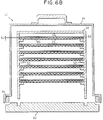
- Figure 6B shows a modification of the arrangement shown in Figure 6A referred to as a closely adjacent vapor drain system embodiment of the present invention.
- a vapor removal element 82 Closely adjacent to each wafer 12, there is a vapor removal element 82, which is approximately congruent with the wafer 12.
- a thin gap 84 Between the wafer and the vapor removal element there is a thin gap 84, defined by a spacer 86.
- the stack of wafers and vapor removal elements have a narrow aspect ratio, typically an 8 mm pitch and a 200 mm diameter. Therefore, in the absence of air flow, a vapor molecule diffusing in the air space between two successive wafers will typically contact a wafer many times before it exits the space. Depending on the surface chemistry, the molecule may adhere to a wafer rather than diffusing out of the stack. This vapor adhesion can be prevented by use of a closely adjacent vapor removal element, as shown in Fig. 6B. For example, between a wafer 12 and its associated vapor removal element 82 there is a gap 84 on the order of 2mm. Therefore the vapor removal element 82 will remove a vapor molecule as it diffuses sideways a root-mean-square distance on the order of 2 mm.
- the internal structure and function of the vapor removal element 82 are generally as described in conjunction with the vapor removal element shown in Figure 3. Also, there may be a clip or other fastening means for attaching a wafer 12 to its associated vapor removal element 82. For loading/unloading, the wafer and associated vapor drain may be handled as single unit, or alternatively, they may be handled individually when not fastened to one another.
- the closely adjacent vapor drain system arrangement shown in Figure 6B provides very good vapor conductance between a wafer 12 and its associated vapor removal element 82. Moreover, this embodiment does not reduce the number of wafers which are contained in the enclosure. However, the arrangement has several limitations. For example, a non-standard machine and procedure is required to load/unload the wafers, particularly to assemble/separate a wafer and its associated vapor removal element. In addition, this embodiment requires numerous thin vapor removal elements 82.
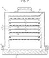
- Figure 7 shows a cross-section of of an alternative embodiment of the present invention which is an inter-leaved vapor drain system.
- the SMIF pod 40 and its parts are generally the same as those shown in Figure 2.
- the gap 84 between each of the sensitive face 14 of wafer 12 and its nearest vapor removal element 82 is on the order of 6mm, so a vapor molecule typically will be absorbed as it travels sideways a root-mean-square distance on the order of 6 mm.
- this embodiment is highly compatible with pre-existing pods, and pre-existing load/unload tools. However, this embodiment reduces the number of wafers contained in an enclosure by one-half.
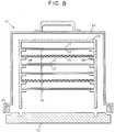
- a SMIF pod 40 is as described above in conjunction with Fig. 2.
- the basic unit is a "trio" comprising a first wafer with sensitive face 14' at the bottom, a two-sided vapor removal element 82, a second wafer 12'' with sensitive face 14''.
- each vapor removal element 82 is located at brackets 88 at a site usually used for locating a wafer, the number of wafers per enclosure is reduced by only one-third. Since every wafer 12', 12'' is near a vapor removal element 82, the vapor conductance is quite large.
- a limitation of the flip-leaved vapor drain system is the requirement of a non-standard machine and procedure to load/unload wafers.
- FIG 9 shows another embodiment of the invention referred to as an integrated sheet vapor drain system global/aero embodiment of the present invention.
- a sheet vapor removal element 54 ( Figure 4) is integrated with an associated wafer 12.
- Each wafer 12 has one side which is the sensitive face 14, and the other side is the substrate for a sheet vapor removal element 54.
- This embodiment removes vapors very much like the inter-leaved vapor drain system shown in Figure 7.
- the sheet vapor removal element may have a pattern with locations where the wafer is handled.
- the seamless unification between vapor removal element 54 and wafer 12 has advantages since the enclosure capacity is not decreased and there is no need for additional effort or machinery to load/unload the vapor drains.
- the integrated sheet vapor removal element may be applied, renewed, removed using equipment and techniques already developed to process wafers.
- the integrated sheet vapor removal element may be permanent, temporary or renewable during wafer processing.
- multiple integrated sheet vapor removal elements may be applied serially during wafer processing.
- Figure 10 shows the aero/global structure of a thermo-buoyant vapor drain (TBVD) system with vertical wafers which is another embodiment of the present invention.
- TSVD thermo-buoyant vapor drain
- the internal air is non-uniformly heated and cooled which causes density differences, buoyant forces, air circulation, vapor convection, and improved vapor conductance within the enclosure 40.
- An enclosure 40 includes a base 42, cover 44, and sealing gasket 46.
- Wafers 12 are located in substantially parallel vertical planes at sites in a stack.
- Retainers 90 hold the wafers 12 in a vertical plane.
- the retainers 90 may be movable or spring loaded to facilitate load/unload and retention of the wafers.
- a heater 102 warms air inside the pod 40, near the bottom of the enclosure.
- an electrical resistance heater 104 is attached to a thermally conductive vane 106 which rests upon a thermal insulator 108 in the base 42.
- cooling means 112 located near the top of the enclosure cools the air inside the enclosure.
- An example of the cooling means is a heat transfer from the warmer air inside the enclosure, through the cover 44 to cooler external air 112. Heating and cooling are graphically represented respectively by arrows 88' and 88''.
- the enclosure may include means for guiding circulation.
- the vane 104 facilitates air heating and aims circulation at the center of the wafer. Also the retainers 90 obstruct some unwanted modes of buoyant circulation.
- Any vapors near the wafer 12 are convected away by circulation 92' to the vicinity of the vapor removal element 30 where the vapors are absorbed.
- the vapor transfer is represented by arrows 94' and 94''.
- Vapor-depleted air circulates back to the wafer 12. Although one air cycle may remove only a fraction of the vapor, nevertheless repeated air cycles iteratively remove vapor, which leads to a steady state condition with low vapor concentration.
- iterated vapor convection enhances vapor conductance from wafer 12 to vapor removal element 30 which makes this embodiment particularly suitable for self-contaminated wafers.
- the power to heat the air may be supplied from an external electrical source, or from an internal electrical battery, or from a thermal reservoir.
- a heater may be inboard of the base, integral with the base, or outboard of the base or inboard, integral or outboard of the cover.
- Yet another embodiment for the heater uses an external source of radiant energy, which passes through a radiation-transparent window into the cover, where it is absorbed by an internal component which generates heat.
- an electrical resistor is used to heat the vane 106.
- the heater may include thermal fins or turning vanes.
- thermal conductors and insulators may be used to radiate energy through the cover into the pod.
- An external heater may be used to radiate energy through the cover into the pod.
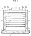
- FIG 11 and Figure 12 are two orthogonal views of a single embodiment of the present invention.
- a SMIF Pod 40 having a base 42, cover 44, and horizontal wafers 12 in a vertical stack 18.
- Heater 102 located near the bottom of the pod warms the air inside the pod as described above.
- air deflectors 114 there are air deflectors 114.
- cooling means 1120 near the top of the SMIF pod cools the air inside the SMIF pod. For example, heat is transferred from the warmer air inside the pod, through the cover 44, to the cooler external air 112. Heating and cooling are represented respectively by arrows 88' and 88'' in Figures 11 and 12.
- Air deflectors 114 guide the circulation over the horizontal wafers 12. In addition, the deflectors 114 obstruct some unwanted modes of buoyant circulation through the enclosure.
- vapor removal element 30 located on the inner wall of the cover 44. Any vapors near the the wafer 12 are convected away by circulation 92''' and 92'''' to the vicinity of the vapor removal element 30 where the vapors are absorbed. Vapor-depleted air circulates back to the wafer 12. Additional vapor removal elements 30 may be located on other inside walls of the cover 44.
- the thermal buoyant vapor drain system arrangements enhance vapor conductance from the stack of wafers to a distant vapor drain, and facilitates wafer load/unload to various degrees. Also, the entire enclosure capacity is useable. Moreover the use of a fan, blower or external air connection is obviated. Considering these features, if the predominant vapor source is located on the wafers, and if the source has significant strength, then a thermal buoyant vapor drain is the preferred embodiment. Although a low power heat source and cool air source are needed, these are often easily provided.
- Fig. 13 shows a flow past vapor drain system embodiment of the present invention.
- the SMIF pod 40 is generally similar to that described above.
- air circulation shown by arrow 120.
- the arrangement may include one or more of a particulate filter 126, an air duct 124 or an air guide 128, such as a diffuser or vanes, to guide the air flow among the wafers 12 in the stack.
- air moves in a cycle through the air mover 122, through the air duct 124, through the particulate filter 126, past the air guide 128, among the wafers 12, past the vapor removal element 30, and back to the air mover 122.
- Air circulation facilitates vapor absorption and particulate filtration in several ways.
- small capacity can be quite adequate for the vapor removal element 30 and for the particulate filter 126. Even though the integrated air flow is extremely large, the total amount of air to clean is quite small.
- circular flow can achieve air which is very vapor-clean and particulate-clean, even with very low removal efficiency per air cycle for the vapor removal element 30 and particulate filter 126, even with a wafer 12 at every site 50.
- RVC relative vapor concentration
- Figure 14 illustrates a "flow through" vapor drain system embodiment of the present invention.
- This embodiment is generally similar to the embodiment described in Figure 13.
- the vapor removal element 130 is porous and located across the duct 124, where air flows through the vapor removal element 130 in the direction of arrow 132.
- the vapor removal element 130 may have a very low efficiency per air cycle to absorb vapor.
- An example is a vapor removal element with an absorber of activated carbon, with especially low density and large porosity.
- the particulate filters 126' and 126'' may have very low efficiency per air cycle to filter out particulates.
- An example is a particulate filter with HEPA material with especially low density and large pores.
- the vapor removal element 130 and particulate filters 126' and 126'' may be pleated to increase the flow area within a compact volume.
- it may be convenient to partly or fully unify the vapor removal element 130 and particulate filters 126' and 126''.
- the particulate filters 126' and 126'' surround the vapor removal element 130 and thus provides a barrier layer in a manner equivalent to absorber layer 32 shown in Figure 3.
- the filter material and absorber material may be placed together before pleating. Nevertheless, in Fig. 14 these elements are shown well separated for graphical clarity.
- a flow through vapor drain system embodiment uses considerable air pressure to enable penetrating flow through a vapor removal element and a particulate filter which allows very aggressive absorption and particulate filtration, but with significant cost and complexity.
- a relevant embodiment is a "leaker" vapor drain system.
- This embodiment includes an aperture in a wall of the pod, and the aperture is covered by a barrier which is vapor-permeable but particulate-blocking.
- the material used is of the type described in relation to the barrier layer 34 in Figure 3.
- the vapor removal element is formed by the barrier and aperture, and operates by vapor diffusion outward from interior air to external air.
- the global/aero structure is an aperture covered by an anti-dust barrier.
- This embodiment can be very simple and inexpensive, and counteracts moderate internal vapor sources. This embodiment works only if the exterior air is vapor clean. However, this embodiment does not counteract external vapor sources, so the embodiment is vulnerable to unexpected changes in the vapor concentration of the external air. The vulnerability can be corrected by adding a vapor absorber, as described below concerning the breather vapor drain system embodiment.
- the breather global/aero structure provides a vapor removal element located across an aperture where internal and external air can be exchanged such as shown in Figure 15.
- the breather vapor removal element provides at least two ports so air can penetrate through the element and provides for removal of vapor from the penetrating air, such as shown in Figure 16.
- a breather vapor drain system embodiment of the present invention In order to preclude vapor contamination caused by breathing in Figure 15, there is shown a breather vapor drain system embodiment of the present invention.
- a SMIF pod 40 has a cover 44, with an aperture 136.
- a breather vapor removal element 138 is located across the aperture 136. Internal air and external air can be exchanged, but any vapors will be absorbed by the breather vapor removal element.
- the internal structure of the vapor removal element 138 is shown in Figure 16. For graphical clarity, the layer thickness is considerably exaggerated in Figures 15, 16 and 17.
- At the center of the vapor removal element 138 is an absorber layer 140 surrounded by barrier layers 142 and 142', surrounded by guard plates 144, 146.
- the guard plates include air channels 148 and 150 respectively.
- the barrier layers are typically HEPA particulate filter material.
- the vapor removal element 138 is located across the aperture 136 in the cover 44.
- the structure, function and construction of vapor removal element generally is analogous to that described above in conjunction with the vapor removal element shown in Figure 3.
- the absorber 140 and barriers layers 142 and 142' are designed with sufficient capacity for the integrated flux of vapor and particulates.
- the air channels 148 and 150 are optimized for vapor transport by air flow through the vapor removal element.
- the embodiment shown in Figure 3 is optimized for vapor movement by diffusion, without microscopic air flow penetrating the vapor removal element.
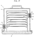
- FIG 17 shows a global/aero structure for an embodiment of the present invention referred to as a purged vapor drain system.
- a SMIF Pod 40 as described above.
- a cover 44 has two or more apertures 136 and 136', each aperture is covered by a respective vapor removal element 138 and 138'.
- means such as an air line or fan, for forcing external air into the pod 40 through one vapor removal element 136'.
- Vapor removal element 136' absorbs any incoming external vapor.
- air is displaced, and flows out through a second vapor removal element 136.
- each vapor removal elements 136 and 136' acts as a breather vapor drain system of the type show in Figure 15 so that external vapors cannot enter the enclosure.
- the internal structure of each vapor removal elements 136 and 136' is as described above in conjunction with Figure 16.
- the absorber 140 and barrier layers 142 and 142' may be further enlarged to hold the larger integrated flux of vapor and particulates and the larger flow of air.
- the absorber and barrier layers may be pleated to provide large vapor-removal capacity in a small volume.
- the vapor removal element can be a chemical sampling device. After prolonged use, the absorber contains accumulated vapors which can be removed and chemically analyzed.
- an absorber material which facilitates chemical extraction and analysis of trapped contamination.
- Tenax brand polymeric absorber which is often used for environmental air sampling and gas chromatography.
- the vapor removal element can be removed from the enclosure, heated to desorb any contamination, which is analyzed in a chromatograph. Since any contamination is removed from the vapor removal element, therefore the element is "regenerated", and the vapor removal element can be reused in an enclosure.
- a vapor drain sampler system can be used to identify and quantitatively measure vapors, leading to elimination of their sources.
Landscapes
- Engineering & Computer Science (AREA)
- Mechanical Engineering (AREA)
- Container, Conveyance, Adherence, Positioning, Of Wafer (AREA)
- Packaging Frangible Articles (AREA)
Applications Claiming Priority (2)
| Application Number | Priority Date | Filing Date | Title |
|---|---|---|---|
| US35999 | 1993-03-23 | ||
| US08/035,999 US5346518A (en) | 1993-03-23 | 1993-03-23 | Vapor drain system |
Publications (2)
| Publication Number | Publication Date |
|---|---|
| EP0617573A1 true EP0617573A1 (fr) | 1994-09-28 |
| EP0617573B1 EP0617573B1 (fr) | 1996-12-04 |
Family
ID=21886014
Family Applications (1)
| Application Number | Title | Priority Date | Filing Date |
|---|---|---|---|
| EP94102707A Expired - Lifetime EP0617573B1 (fr) | 1993-03-23 | 1994-02-23 | Système de drainage de vapeur |
Country Status (4)
| Country | Link |
|---|---|
| US (1) | US5346518A (fr) |
| EP (1) | EP0617573B1 (fr) |
| JP (1) | JP2601990B2 (fr) |
| DE (1) | DE69401023D1 (fr) |
Cited By (11)
| Publication number | Priority date | Publication date | Assignee | Title |
|---|---|---|---|---|
| EP1589565A1 (fr) * | 2004-04-21 | 2005-10-26 | Alcatel | Dispositif pour le transport de substrats sous atmosphère controlée |
| EP1589564A1 (fr) * | 2004-04-21 | 2005-10-26 | Alcatel | Enveloppe de transport à protection par effet thermophorèse |
| EP1093395A4 (fr) * | 1998-05-21 | 2006-11-15 | Advanced Tech Materials | Dispositif de production et de stockage d'un gaz au moyen d'un absorbant pour la distribution d'un gaz de haute purete |
| WO2007019105A1 (fr) * | 2005-08-03 | 2007-02-15 | Entegris, Inc. | Conteneur de transfert |
| EP1487009A4 (fr) * | 2002-11-26 | 2007-04-11 | Disco Corp | Cassette de stockage de multiples feuilles de plaquettes semi-conductrices |
| EP1548820A4 (fr) * | 2002-09-11 | 2007-06-06 | Shinetsu Polymer Co | Receptacle de stockage de substrats |
| EP1035574A4 (fr) * | 1997-11-28 | 2007-11-28 | Ebara Corp | Boite de transfert d'une tranche en semi-conducteur |
| EP2035320A4 (fr) * | 2006-06-19 | 2010-07-28 | Entegris Inc | Système de purge destockage de réticule |
| EP3018530A4 (fr) * | 2013-07-03 | 2017-01-25 | Murata Machinery, Ltd. | Récipient de stockage |
| CN109095005A (zh) * | 2018-06-29 | 2018-12-28 | 池州市清心信息技术服务有限公司 | 一种竹家具防霉装置 |
| CN110893935A (zh) * | 2019-12-02 | 2020-03-20 | 安庆银亿轴承有限公司 | 一种精密轴承存放箱 |
Families Citing this family (68)
| Publication number | Priority date | Publication date | Assignee | Title |
|---|---|---|---|---|
| JP2976755B2 (ja) * | 1993-08-06 | 1999-11-10 | 株式会社ダイフク | 荷物保管装置 |
| US5417743A (en) * | 1994-01-21 | 1995-05-23 | W. L. Gore & Associates, Inc. | Self-adhesive vent filter and adsorbent assembly with a diffusion tube |
| JP2601999B2 (ja) * | 1994-07-29 | 1997-04-23 | インターナショナル・ビジネス・マシーンズ・コーポレイション | ディスクドライブ装置 |
| US5582411A (en) * | 1994-12-13 | 1996-12-10 | International Business Machines Corporation | Scavenging compound infiltrated gasket |
| US5833726A (en) * | 1995-05-26 | 1998-11-10 | Extraction System, Inc. | Storing substrates between process steps within a processing facility |
| DE19540963C2 (de) * | 1995-11-03 | 1999-05-20 | Jenoptik Jena Gmbh | Transportbehälter für scheibenförmige Objekte |
| FR2747112B1 (fr) * | 1996-04-03 | 1998-05-07 | Commissariat Energie Atomique | Dispositif de transport d'objets plats et procede de transfert de ces objets entre ledit dispositif et une machine de traitement |
| US5709065A (en) * | 1996-07-31 | 1998-01-20 | Empak, Inc. | Desiccant substrate package |
| US5843196A (en) * | 1997-01-21 | 1998-12-01 | International Business Machines Corporation | Ultra-clean transport carrier |
| US6031685A (en) * | 1997-07-11 | 2000-02-29 | Seagate Technology, Inc. | Information storage systems comprising a liquid bearing maintained by adsorption isotherm |
| JP3933394B2 (ja) * | 1997-12-03 | 2007-06-20 | 株式会社荏原製作所 | クリーンボックス |
| US6319297B1 (en) * | 1998-03-27 | 2001-11-20 | Asyst Technologies, Inc. | Modular SMIF pod breather, adsorbent, and purge cartridges |
| US6152885A (en) * | 1998-04-30 | 2000-11-28 | Medtronic, Inc. | Barometric pressure sensor for use with implantable absolute pressure sensor |
| US5997614A (en) * | 1998-07-13 | 1999-12-07 | Donaldson Company, Inc. | Filter with diffusion channel and methods of making and using the filter |
| JP3916380B2 (ja) * | 1999-07-06 | 2007-05-16 | 株式会社荏原製作所 | 基板搬送容器待機ステーション |
| US6214070B1 (en) | 1999-07-19 | 2001-04-10 | Maxtor Corporation | Disk drive filter |
| US6401929B2 (en) * | 2000-01-12 | 2002-06-11 | Agere Systems Guardian Corp. | Insert for use in transporting a wafer carrier |
| JP2001284443A (ja) * | 2000-04-03 | 2001-10-12 | Nec Corp | 半導体基板の保管搬送容器、半導体装置の製造方法 |
| JP3939101B2 (ja) * | 2000-12-04 | 2007-07-04 | 株式会社荏原製作所 | 基板搬送方法および基板搬送容器 |
| JP2002313867A (ja) * | 2001-02-09 | 2002-10-25 | Toshiba Corp | 半導体装置の製造方法 |
| EP1373099A4 (fr) * | 2001-04-01 | 2008-05-28 | Entegris Inc | Insert de plaquette fine |
| US6875282B2 (en) | 2001-05-17 | 2005-04-05 | Ebara Corporation | Substrate transport container |
| JP2003007813A (ja) * | 2001-06-20 | 2003-01-10 | Nec Corp | 半導体ウエハの保管ボックス、運搬装置、運搬方法及び保管倉庫 |
| EP1428287B1 (fr) * | 2001-08-16 | 2008-10-29 | Communications & Power Industries, Inc. | Fenetre pour guides d'onde destinee a empecher des degats dus a la presence d'objets etrangers |
| US6637998B2 (en) | 2001-10-01 | 2003-10-28 | Air Products And Chemicals, Inc. | Self evacuating micro environment system |
| JP2004210421A (ja) | 2002-12-26 | 2004-07-29 | Semiconductor Energy Lab Co Ltd | 製造システム、並びに処理装置の操作方法 |
| TW594906B (en) * | 2003-05-14 | 2004-06-21 | Au Optronics Corp | Cassette in a load-lock |
| US6913654B2 (en) * | 2003-06-02 | 2005-07-05 | Mykrolis Corporation | Method for the removal of airborne molecular contaminants using water gas mixtures |
| WO2004109748A2 (fr) * | 2003-06-05 | 2004-12-16 | Palbam Class Ltd. | Ratelier de support pour nacelle unifiée à ouverture frontale |
| US20050108996A1 (en) * | 2003-11-26 | 2005-05-26 | Latham Steven R. | Filter system for an electronic equipment enclosure |
| FR2865314B1 (fr) * | 2004-01-20 | 2006-04-28 | Cit Alcatel | Station de controle et de purge de mini-environnement |
| US20050155874A1 (en) * | 2004-01-21 | 2005-07-21 | Noah Chen | SMIF box and loading system of reticle |
| KR20120099802A (ko) | 2004-02-05 | 2012-09-11 | 엔테그리스, 아이엔씨. | 웨이퍼 반송 용기의 세정 |
| US7328727B2 (en) | 2004-04-18 | 2008-02-12 | Entegris, Inc. | Substrate container with fluid-sealing flow passageway |
| DE102004063912B4 (de) * | 2004-04-22 | 2007-09-20 | Siltronic Ag | Verfahren zum versandfertigen Verpacken von Halbleiterscheiben |
| TW200540922A (en) * | 2004-06-04 | 2005-12-16 | Kondoh Ind Ltd | Air-purifying equipment in a semiconductor wafer container |
| TWM276316U (en) * | 2004-08-17 | 2005-09-21 | Tzu-Lung Fu | Device having a function of absorbing gas |
| US7400383B2 (en) * | 2005-04-04 | 2008-07-15 | Entegris, Inc. | Environmental control in a reticle SMIF pod |
| US11024527B2 (en) * | 2005-06-18 | 2021-06-01 | Frederick A. Flitsch | Methods and apparatus for novel fabricators with Cleanspace |
| US20070076292A1 (en) * | 2005-09-27 | 2007-04-05 | Taiwan Semiconductor Manufacturing Company, Ltd. | Fully electric field shielding reticle pod |
| US20070144118A1 (en) * | 2005-12-22 | 2007-06-28 | Alvarez Daniel Jr | Purging of a wafer conveyance container |
| TWI298185B (en) * | 2006-01-25 | 2008-06-21 | Promos Technologies Inc | Wafer-transferring pod capable of monitoring process environment |
| US20080060974A1 (en) * | 2006-02-21 | 2008-03-13 | Taiwan Semiconductor Manufacturing Company, Ltd. | Mask carrier treatment to prevent haze and ESD damage |
| KR101494024B1 (ko) * | 2007-02-28 | 2015-02-16 | 엔테그리스, 아이엔씨. | 기판 컨테이너를 위한 퍼지 시스템 |
| JP5073565B2 (ja) * | 2007-04-16 | 2012-11-14 | ミライアル株式会社 | カートリッジ型ケミカルアブソーバー |
| TWM331514U (en) * | 2007-11-15 | 2008-05-01 | Gudeng Prec Industral Co Ltd | Storage apparatus for storing semiconductor element or reticle |
| JP5613367B2 (ja) * | 2008-01-18 | 2014-10-22 | 大日商事株式会社 | ケミカルフィルタ及びその梱包体並びにレチクル保管ボックス |
| CN102017119B (zh) * | 2008-03-13 | 2014-01-01 | 安格斯公司 | 具有管状环境控制部件的晶圆容器 |
| US7938269B2 (en) * | 2008-11-11 | 2011-05-10 | Taiwan Semiconductor Manufacturing Co., Ltd. | Ventilated front-opening unified pod |
| US8175757B2 (en) * | 2009-09-10 | 2012-05-08 | Avaya Inc. | Self-cleaning chassis |
| JP5403555B2 (ja) * | 2010-03-09 | 2014-01-29 | 信越ポリマー株式会社 | 基板収納容器及びその搬送設備 |
| US8377182B2 (en) * | 2010-05-14 | 2013-02-19 | Brady Worldwide, Inc. | Gas anti diffusion assemblies |
| TW201141768A (en) * | 2010-05-19 | 2011-12-01 | He zhong shan | Method of reducing photomask pollution and photomask storage device thereof |
| TW201302573A (zh) | 2011-05-03 | 2013-01-16 | 安堤格里斯公司 | 具有微粒屏蔽之晶圓容器 |
| US8544651B2 (en) * | 2012-01-20 | 2013-10-01 | Taiwan Semiconductor Manufacturing Company, Ltd. | Wafer transfer pod for reducing wafer particulate contamination |
| KR20130095495A (ko) * | 2012-02-20 | 2013-08-28 | 삼성전자주식회사 | 반도체 기판 적재용 보트 |
| JP2013251348A (ja) * | 2012-05-30 | 2013-12-12 | Tokyo Ohka Kogyo Co Ltd | 基板保持装置及び基板処理装置 |
| US11462437B2 (en) | 2013-01-05 | 2022-10-04 | Frederick A. Flitsch | Customized smart devices and touchscreen devices and cleanspace manufacturing methods to make them |
| US12189828B2 (en) | 2013-01-05 | 2025-01-07 | Frederick A. Flitsch | Customized smart devices and touchscreen devices and cleanspace manufacturing methods to make them |
| EP2792471B1 (fr) * | 2013-04-16 | 2018-01-31 | Stratec Consumables GmbH | Pièces en polymère |
| KR20160052645A (ko) * | 2013-09-06 | 2016-05-12 | 엔테그리스, 아이엔씨. | 개선된 고체 게터를 갖춘 기판 격납고 |
| US9881826B2 (en) * | 2014-10-24 | 2018-01-30 | Lam Research Corporation | Buffer station with single exit-flow direction |
| KR20220053034A (ko) * | 2015-05-12 | 2022-04-28 | 엔테그리스, 아이엔씨. | 외부 수동 게터 모듈을 구비하는 웨이퍼 컨테이너 |
| KR20220044187A (ko) * | 2019-06-06 | 2022-04-06 | 애리스 컴포지트 아이엔씨. | 예비성형체 충전물 카트리지 및 이를 위한 시리얼화 방법 |
| US11651982B2 (en) * | 2019-10-11 | 2023-05-16 | Winbond Electronics Corp. | Drying block structure and storage device |
| WO2021092396A1 (fr) | 2019-11-08 | 2021-05-14 | Entegris, Inc. | Support de substance de régulation de l'environnement |
| CN112278613B (zh) * | 2020-10-29 | 2022-02-18 | 瑞昌市兴海王子家具有限公司 | 一种床垫叠放装置 |
| US20230030188A1 (en) * | 2021-07-22 | 2023-02-02 | Entegris, Inc. | Adsorbents and methods for reducing contamination in wafer container microenvironments |
Citations (3)
| Publication number | Priority date | Publication date | Assignee | Title |
|---|---|---|---|---|
| EP0151336A2 (fr) * | 1983-09-28 | 1985-08-14 | Hewlett-Packard Company | Système de traitement de circuits intégrés |
| US4739882A (en) * | 1986-02-13 | 1988-04-26 | Asyst Technologies | Container having disposable liners |
| EP0512579A1 (fr) * | 1986-11-25 | 1992-11-11 | Hitachi, Ltd. | Emballage d'éléments semi-conducteurs |
Family Cites Families (20)
| Publication number | Priority date | Publication date | Assignee | Title |
|---|---|---|---|---|
| US3631423A (en) * | 1969-06-13 | 1971-12-28 | Burroughs Corp | Self-purging disk system |
| US3710540A (en) * | 1970-11-25 | 1973-01-16 | Burroughs Corp | Self-purging disk system having air flow guide means |
| US3846835A (en) * | 1973-05-29 | 1974-11-05 | Sperry Rand Corp | Clean air system for magnetic storage disk pack |
| GB2024495B (en) * | 1978-05-16 | 1982-12-22 | Burroughs Corp | Record-disc cover having air filtration section |
| US4339777A (en) * | 1980-04-10 | 1982-07-13 | Minnesota Mining And Manufacturing Company | Air-flow system for a disk file |
| JPS57200971A (en) * | 1981-06-01 | 1982-12-09 | Hitachi Ltd | Magnetic disk storage device |
| US4489356A (en) * | 1982-06-24 | 1984-12-18 | Atasi Corporation | Enclosed disk drive with improved air filtration system |
| US4532970A (en) * | 1983-09-28 | 1985-08-06 | Hewlett-Packard Company | Particle-free dockable interface for integrated circuit processing |
| US4534389A (en) * | 1984-03-29 | 1985-08-13 | Hewlett-Packard Company | Interlocking door latch for dockable interface for integrated circuit processing |
| US4620248A (en) * | 1984-09-04 | 1986-10-28 | Magnetic Peripherals Inc. | Apparatus for controlling humidity in a disk drive |
| US4772300A (en) * | 1985-04-04 | 1988-09-20 | Multiform Desiccants, Inc. | Adsorbent cartridge |
| US4666479A (en) * | 1985-07-18 | 1987-05-19 | Tensho Electric Industrial Co., Ltd. | Semiconductor wafer container |
| US4684510A (en) * | 1985-12-20 | 1987-08-04 | Hewlett-Packard Company | Method and apparatus for prevention of atmospheric corrosion of electronic equipment |
| US4721207A (en) * | 1986-04-28 | 1988-01-26 | Tensho Electric Industrial Co., Ltd. | Hard disk container |
| FR2610846A1 (fr) * | 1987-02-17 | 1988-08-19 | Air Liquide | Element filtrant pour dispositif d'event et dispositif comportant un tel element |
| US5057217A (en) * | 1987-06-25 | 1991-10-15 | W. L. Gore & Associates, Inc. | Integral supported filter medium assembly |
| US5047348A (en) * | 1989-04-10 | 1991-09-10 | Massachusetts Institute Of Technology | Apparatus for housing radioactive items during incubation |
| JPH02281495A (ja) * | 1989-04-20 | 1990-11-19 | Mitsubishi Electric Corp | 磁気ディスク装置 |
| US5030260A (en) * | 1989-12-04 | 1991-07-09 | International Business Machines Corporation | Disk drive breather filter |
| JP2803688B2 (ja) * | 1990-05-24 | 1998-09-24 | インターナショナル・ビジネス・マシーンズ・コーポレイション | 磁気ディスク記憶装置 |
-
1993
- 1993-03-23 US US08/035,999 patent/US5346518A/en not_active Expired - Lifetime
-
1994
- 1994-01-14 JP JP6014959A patent/JP2601990B2/ja not_active Expired - Fee Related
- 1994-02-23 DE DE69401023T patent/DE69401023D1/de not_active Expired - Lifetime
- 1994-02-23 EP EP94102707A patent/EP0617573B1/fr not_active Expired - Lifetime
Patent Citations (3)
| Publication number | Priority date | Publication date | Assignee | Title |
|---|---|---|---|---|
| EP0151336A2 (fr) * | 1983-09-28 | 1985-08-14 | Hewlett-Packard Company | Système de traitement de circuits intégrés |
| US4739882A (en) * | 1986-02-13 | 1988-04-26 | Asyst Technologies | Container having disposable liners |
| EP0512579A1 (fr) * | 1986-11-25 | 1992-11-11 | Hitachi, Ltd. | Emballage d'éléments semi-conducteurs |
Cited By (19)
| Publication number | Priority date | Publication date | Assignee | Title |
|---|---|---|---|---|
| EP1035574A4 (fr) * | 1997-11-28 | 2007-11-28 | Ebara Corp | Boite de transfert d'une tranche en semi-conducteur |
| EP1093395A4 (fr) * | 1998-05-21 | 2006-11-15 | Advanced Tech Materials | Dispositif de production et de stockage d'un gaz au moyen d'un absorbant pour la distribution d'un gaz de haute purete |
| US7823730B2 (en) | 2002-09-11 | 2010-11-02 | Shin-Etsu Polymer Co., Ltd. | Substrate storage container |
| EP1548820A4 (fr) * | 2002-09-11 | 2007-06-06 | Shinetsu Polymer Co | Receptacle de stockage de substrats |
| EP1487009A4 (fr) * | 2002-11-26 | 2007-04-11 | Disco Corp | Cassette de stockage de multiples feuilles de plaquettes semi-conductrices |
| US7325692B2 (en) | 2002-11-26 | 2008-02-05 | Disco Corporation | Cassette having separation plates for storing a plurality of semiconductor wafers |
| US7735648B2 (en) | 2004-04-21 | 2010-06-15 | Alcatel | Transport pod with protection by the thermophoresis effect |
| EP1589564A1 (fr) * | 2004-04-21 | 2005-10-26 | Alcatel | Enveloppe de transport à protection par effet thermophorèse |
| FR2869452A1 (fr) * | 2004-04-21 | 2005-10-28 | Alcatel Sa | Dispositif pour le transport de substrats sous atmosphere controlee |
| EP1589565A1 (fr) * | 2004-04-21 | 2005-10-26 | Alcatel | Dispositif pour le transport de substrats sous atmosphère controlée |
| US7694700B2 (en) | 2004-04-21 | 2010-04-13 | Alcatel | Apparatus for transporting substrates under a controlled atmosphere |
| FR2869451A1 (fr) * | 2004-04-21 | 2005-10-28 | Alcatel Sa | Enveloppe de transport a protection par effet thermophorese |
| WO2007019105A1 (fr) * | 2005-08-03 | 2007-02-15 | Entegris, Inc. | Conteneur de transfert |
| EP2035320A4 (fr) * | 2006-06-19 | 2010-07-28 | Entegris Inc | Système de purge destockage de réticule |
| US8776841B2 (en) | 2006-06-19 | 2014-07-15 | Entegris, Inc. | System for purging reticle storage |
| EP3018530A4 (fr) * | 2013-07-03 | 2017-01-25 | Murata Machinery, Ltd. | Récipient de stockage |
| US9841671B2 (en) | 2013-07-03 | 2017-12-12 | Murata Machinery, Ltd. | Storage container |
| CN109095005A (zh) * | 2018-06-29 | 2018-12-28 | 池州市清心信息技术服务有限公司 | 一种竹家具防霉装置 |
| CN110893935A (zh) * | 2019-12-02 | 2020-03-20 | 安庆银亿轴承有限公司 | 一种精密轴承存放箱 |
Also Published As
| Publication number | Publication date |
|---|---|
| US5346518A (en) | 1994-09-13 |
| EP0617573B1 (fr) | 1996-12-04 |
| JPH0794577A (ja) | 1995-04-07 |
| JP2601990B2 (ja) | 1997-04-23 |
| DE69401023D1 (de) | 1997-01-16 |
Similar Documents
| Publication | Publication Date | Title |
|---|---|---|
| EP0617573B1 (fr) | Système de drainage de vapeur | |
| JP7351543B2 (ja) | インクジェットプリンタ | |
| CN100449682C (zh) | 衬底传送容器 | |
| US6051169A (en) | Vacuum baking process | |
| TWI688533B (zh) | 被動吸氣匣盒及前開式半導體晶圓容置盒總成 | |
| US6875282B2 (en) | Substrate transport container | |
| TWI289534B (en) | Substrate storage container | |
| JP4937993B2 (ja) | 外気導入・排出設備 | |
| US10035351B2 (en) | Ink delivery systems and methods | |
| TW202012288A (zh) | 基板容器之膜擴散器 | |
| KR20010078077A (ko) | 기판용기 | |
| CN108290105B (zh) | 用于闭合件保护的吸附剂通气装置 | |
| JP2002359180A (ja) | ガス循環システム | |
| TWI670388B (zh) | 環境控制鍍膜系統 | |
| JP2002122382A (ja) | 基板容器 | |
| TW201703174A (zh) | 半導體晶圓載具總成、門總成、基板容器與吸氣劑模組之組合及降低前開式容器內污染物濃度之方法 | |
| JP2006005072A (ja) | 基板搬送保管容器及びその使用方法 | |
| TWI764113B (zh) | 低粒氣體封裝系統與方法 | |
| Muller | Comparison of chemical filters for the control of airborne molecular contamination | |
| JP2000189736A (ja) | エアフィルタ装置 | |
| JP2004144501A (ja) | 分析用試料板体の収納装置 | |
| JPH1167889A (ja) | 半導体基板の保管ボックス |
Legal Events
| Date | Code | Title | Description |
|---|---|---|---|
| PUAI | Public reference made under article 153(3) epc to a published international application that has entered the european phase |
Free format text: ORIGINAL CODE: 0009012 |
|
| AK | Designated contracting states |
Kind code of ref document: A1 Designated state(s): DE FR GB |
|
| 17P | Request for examination filed |
Effective date: 19950117 |
|
| 17Q | First examination report despatched |
Effective date: 19950220 |
|
| GRAG | Despatch of communication of intention to grant |
Free format text: ORIGINAL CODE: EPIDOS AGRA |
|
| GRAH | Despatch of communication of intention to grant a patent |
Free format text: ORIGINAL CODE: EPIDOS IGRA |
|
| GRAH | Despatch of communication of intention to grant a patent |
Free format text: ORIGINAL CODE: EPIDOS IGRA |
|
| GRAA | (expected) grant |
Free format text: ORIGINAL CODE: 0009210 |
|
| AK | Designated contracting states |
Kind code of ref document: B1 Designated state(s): DE FR GB |
|
| REF | Corresponds to: |
Ref document number: 69401023 Country of ref document: DE Date of ref document: 19970116 |
|
| PGFP | Annual fee paid to national office [announced via postgrant information from national office to epo] |
Ref country code: FR Payment date: 19970210 Year of fee payment: 4 |
|
| PG25 | Lapsed in a contracting state [announced via postgrant information from national office to epo] |
Ref country code: DE Effective date: 19970305 |
|
| ET | Fr: translation filed | ||
| PLBE | No opposition filed within time limit |
Free format text: ORIGINAL CODE: 0009261 |
|
| STAA | Information on the status of an ep patent application or granted ep patent |
Free format text: STATUS: NO OPPOSITION FILED WITHIN TIME LIMIT |
|
| 26N | No opposition filed | ||
| PG25 | Lapsed in a contracting state [announced via postgrant information from national office to epo] |
Ref country code: GB Free format text: LAPSE BECAUSE OF NON-PAYMENT OF DUE FEES Effective date: 19980223 |
|
| PG25 | Lapsed in a contracting state [announced via postgrant information from national office to epo] |
Ref country code: FR Free format text: THE PATENT HAS BEEN ANNULLED BY A DECISION OF A NATIONAL AUTHORITY Effective date: 19980228 |
|
| GBPC | Gb: european patent ceased through non-payment of renewal fee |
Effective date: 19980223 |
|
| REG | Reference to a national code |
Ref country code: FR Ref legal event code: ST |