EP0618043A1 - Gegenstand mit polykristallinem Diamant, und Verfahren zum Formen eines Diamants - Google Patents
Gegenstand mit polykristallinem Diamant, und Verfahren zum Formen eines Diamants Download PDFInfo
- Publication number
- EP0618043A1 EP0618043A1 EP94301902A EP94301902A EP0618043A1 EP 0618043 A1 EP0618043 A1 EP 0618043A1 EP 94301902 A EP94301902 A EP 94301902A EP 94301902 A EP94301902 A EP 94301902A EP 0618043 A1 EP0618043 A1 EP 0618043A1
- Authority
- EP
- European Patent Office
- Prior art keywords
- polyd
- template
- feature
- article
- diamond
- Prior art date
- Legal status (The legal status is an assumption and is not a legal conclusion. Google has not performed a legal analysis and makes no representation as to the accuracy of the status listed.)
- Withdrawn
Links
- 229910003460 diamond Inorganic materials 0.000 title claims abstract description 28
- 239000010432 diamond Substances 0.000 title claims abstract description 28
- 238000000034 method Methods 0.000 title claims abstract description 28
- 238000007493 shaping process Methods 0.000 title description 5
- 239000000463 material Substances 0.000 claims abstract description 19
- 230000003287 optical effect Effects 0.000 claims abstract description 12
- 238000002844 melting Methods 0.000 claims abstract description 8
- 230000008018 melting Effects 0.000 claims abstract description 8
- 229910052761 rare earth metal Inorganic materials 0.000 claims abstract description 7
- 150000002910 rare earth metals Chemical class 0.000 claims abstract description 7
- 229910052684 Cerium Inorganic materials 0.000 claims abstract description 5
- 229910052746 lanthanum Inorganic materials 0.000 claims abstract description 5
- 239000002243 precursor Substances 0.000 claims description 23
- 229910052751 metal Inorganic materials 0.000 claims description 10
- 239000002184 metal Substances 0.000 claims description 10
- 229910052742 iron Inorganic materials 0.000 claims description 6
- 229910052748 manganese Inorganic materials 0.000 claims description 5
- 238000004519 manufacturing process Methods 0.000 claims description 3
- 230000001131 transforming effect Effects 0.000 claims description 2
- 230000015572 biosynthetic process Effects 0.000 abstract description 7
- 238000005498 polishing Methods 0.000 abstract description 4
- 238000003491 array Methods 0.000 abstract description 3
- 238000003486 chemical etching Methods 0.000 abstract description 3
- 238000000608 laser ablation Methods 0.000 abstract description 2
- 238000010028 chemical finishing Methods 0.000 abstract 1
- 238000007373 indentation Methods 0.000 description 5
- OKTJSMMVPCPJKN-UHFFFAOYSA-N Carbon Chemical compound [C] OKTJSMMVPCPJKN-UHFFFAOYSA-N 0.000 description 4
- 229910052799 carbon Inorganic materials 0.000 description 4
- 238000005229 chemical vapour deposition Methods 0.000 description 4
- 239000013078 crystal Substances 0.000 description 4
- PNEYBMLMFCGWSK-UHFFFAOYSA-N aluminium oxide Inorganic materials [O-2].[O-2].[O-2].[Al+3].[Al+3] PNEYBMLMFCGWSK-UHFFFAOYSA-N 0.000 description 3
- 229910052593 corundum Inorganic materials 0.000 description 3
- 238000005530 etching Methods 0.000 description 3
- 238000010438 heat treatment Methods 0.000 description 3
- 229910001845 yogo sapphire Inorganic materials 0.000 description 3
- 239000002253 acid Substances 0.000 description 2
- 229910045601 alloy Inorganic materials 0.000 description 2
- 239000000956 alloy Substances 0.000 description 2
- 238000001816 cooling Methods 0.000 description 2
- 229910052759 nickel Inorganic materials 0.000 description 2
- 239000000843 powder Substances 0.000 description 2
- 239000000758 substrate Substances 0.000 description 2
- 229910000831 Steel Inorganic materials 0.000 description 1
- 238000007796 conventional method Methods 0.000 description 1
- 230000001419 dependent effect Effects 0.000 description 1
- -1 e.g. Substances 0.000 description 1
- 229910001651 emery Inorganic materials 0.000 description 1
- 238000009499 grossing Methods 0.000 description 1
- 239000007943 implant Substances 0.000 description 1
- 239000011261 inert gas Substances 0.000 description 1
- 229910001338 liquidmetal Inorganic materials 0.000 description 1
- 239000000203 mixture Substances 0.000 description 1
- 229910052750 molybdenum Inorganic materials 0.000 description 1
- 229910052697 platinum Inorganic materials 0.000 description 1
- 239000010959 steel Substances 0.000 description 1
- 239000000126 substance Substances 0.000 description 1
- 229910052719 titanium Inorganic materials 0.000 description 1
Images


Classifications
-
- G—PHYSICS
- G02—OPTICS
- G02B—OPTICAL ELEMENTS, SYSTEMS OR APPARATUS
- G02B1/00—Optical elements characterised by the material of which they are made; Optical coatings for optical elements
- G02B1/02—Optical elements characterised by the material of which they are made; Optical coatings for optical elements made of crystals, e.g. rock-salt, semi-conductors
-
- B—PERFORMING OPERATIONS; TRANSPORTING
- B24—GRINDING; POLISHING
- B24D—TOOLS FOR GRINDING, BUFFING OR SHARPENING
- B24D3/00—Physical features of abrasive bodies, or sheets, e.g. abrasive surfaces of special nature; Abrasive bodies or sheets characterised by their constituents
Definitions
- This invention pertains to polycrystalline diamond (herein polyD) film, and to methods of shaping the film.
- PolyD films typically prepared by chemical vapor deposition (CVD), have received considerable attention in recent years, because of their remarkable properties. These include high thermal conductivity, optical transparency, high refractive index, mechanical hardness and chemical inertness.
- PolyD film comprises many crystallites, and there will always be present crystallites that have one of their hard directions approximately oriented in the removal direction, and thus cannot be removed easily by conventional means. It is principally for this reason that removal of material from polyD films has been problematical.
- U.S. Patent application Serial No. 07/822,470 filed January 17, 1992 for J. E. Graebner et al., discloses a method of removing material from a polyD film that comprises maintaining the film in intimate contact with Fe, Ni, Mn or Ti at 600-1100°C. See also S. Jin et al., Applied Physics Letters , Vol. 60, p. 1948 (1992), and S. Jin et al., Diamond Films and Related Materials , Vol. 1, p. 949 (1992). The required intimate contact typically is attained through application of pressure during the high temperature treatment.
- U.S. Patent application Serial No. 07/908,130 filed July 2, 1992 for W. C.
- Dautremont-Smith et al. discloses thinning of polyD film by contacting the film with molten or partially molten metal that dissolves carbon, exemplarily a rare earth (e.g., La or Ce) or mixture of rare earths. It also discloses that portions of a surface of the polyD film can be protected by masks against the liquid metal. See also U.S. Patent application Serial No. 07/955,634, filed October 2, 1992 for J. E.
- Graebner et al. which discloses use of a molten or partially molten alloy of a rare earth metal (e.g., Ce) and a melting point-lowering metal, e.g., Ni, permitting a drastic reduction in thinning temperature, as compared to the method of the '130 application.
- a rare earth metal e.g., Ce
- a melting point-lowering metal e.g., Ni
- U.K. Patent application GB 2,061,904A discloses shaping a diamond body (not polyD) by contacting the body with an appropriately shaped metal (preferably Fe, Ni, Pt or alloys thereof) "template" at a temperature in the range 600-1800°C in vacuum, inert gas atmosphere, or in an atmosphere which does not react with diamond but reacts with carbon dissolved in the metal.
- an appropriately shaped metal preferably Fe, Ni, Pt or alloys thereof
- planar surface of the precursor polyD film we mean a surface that at most has only the, typically unavoidable, microscopic irregularities found in as-grown polyD films, but does not have any macroscopic non-planar features.
- non-planar surface we mean a surface that comprises one or more macroscopic (at least one lateral dimension typically greater than 100 ⁇ m) features that extend above or below the nominal surface of the body.
- the nominal surface is the planar portion of the non-planar surface.
- a feature in or on a non-planar polyD surface is a "substantial replica" of a feature in a template body if the shape and size of the feature, in or on the polyD surface, substantially correspond to the shape and relevant size of the feature in the template body.
- One-to-one correspondence typically will not be attained, requiring pre-determination of template feature shape and size that will result in the desired polyD feature shape and size. This can typically be accomplished by a minor amount of routine experimentation. It will be recognized that typically a convex (concave) template feature corresponds to a concave (convex) polyD feature.
- the invention is defined by the claims.
- the invention is embodied in a method of making an article that comprises a polyD film having a non-planar surface, e.g., a surface that comprises one or more lenticular (convex or concave) portions.
- the method comprises providing a precursor diamond body that has a substantially planar surface, and forming the desired diamond body from the precursor body by a process that comprises removing diamond material from the precursor body by contacting said surface of the precursor body with a hot template.
- the precursor body is a polyD film
- the template comprises a template body that comprises a metal selected from the group consisting of the rare earth metals (atomic number 57-71), Mn and Fe.
- the template body will typically contain at least 20 (preferably at least 50) atomic percent of rare earth metal, Mn and/or Fe.
- the preferred rare earth metals are Ce and La.
- the template body has a non-planar surface and is maintained, during said contacting step, at a temperature (or temperatures) below (preferably at least 20°C below) the melting temperature of said template body.
- the method further comprises maintaining the template body in intimate contact with at least a portion of said surface of the precursor body for a time (exemplarily in the range 1 - 1000 hours) effective for transforming said substantially planar surface of the precursor body into a non-planar surface that comprises a substantial replica of said non-planar surface of the template body.
- the replica typically, but not necessarily, is a negative one. Further processing (e.g., smoothing by laser ablation or other known method) of the feature in/on the polyD surface may be appropriate and is contemplated.
- the heat treatment preferably is carried out in an inert or reducing atmosphere, e.g., in Ar, He, N2 or H2. At least in some cases (e.g., if the melting point of the template body changes with the amount of dissolved carbon in the body) it may be advantageous to appropriately change the temperature during the course of the heat treatment, so that melting (or excessive softening) of the template body is avoided, and so that a relatively high reaction rate is maintained.
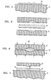
- FIGS. 1-4 schematically depict aspects of the inventive method.
- Numeral 10 designates an optional substrate, 11 a (planar) polyD precursor body, and 12 a template body that comprises a non-planar surface facing the polyD film, with the surface having concave features 122, 123 and 124 and a planar portion 121.
- FIG. 1 depicts the arrangement before the template body is brought into contact with the precursor body
- FIG. 2 shows the template body in intimate contact with the precursor body (intimate contact exemplarily is achieved by means of applied force, indicated by arrows)
- FIG. 3 shows the arrangement just prior to completion of material removal from the polyD film (numeral 30 refers to the polyD body formed from the precursor body by selective removal of material)
- FIG. 10 designates an optional substrate
- 11 a (planar) polyD precursor body
- 12 a template body that comprises a non-planar surface facing the polyD film, with the surface having concave features 122, 123 and 124 and a planar portion
- the interface between the polyD body (e.g., 11, 50) and the template body (e.g., 12, 51, 52) corresponds to the interface between essentially pure polyD and metal (e.g., Ce)-containing material (e.g., substantially pure Ce in FIG. 2, and C-containing Ce in FIGS. 3 and 6).
- metal e.g., Ce
- FIGS. 5 and 6 schematically depict another exemplary embodiment of the invention, wherein numeral 50 refers to a freestanding polyD precursor body, 51 and 52 to template bodies, and 60 to the resulting polyD body just prior to completion of the selective removal of diamond material.
- FIG. 7 schematically depicts a polyD body 70 that comprises a concave feature 71, that extends below the "nominal" surface 74 and also depicts template body 72 having a non-planar surface that comprises convex feature 73.
- FIGS. 1-7 illustrate formation of non-planar surfaces that comprise features (concave or convex) that substantially are replicas of the non-planar portion of the template body in contact with the polyD surface.
- FIGS. 8 and 9 schematically illustrate an embodiment of the invention that can result in formation of a substantial replica of a non-planar feature that is not in contact with the polyD surface.
- numeral 80 refers to the polyD precursor body, and 81 to the template body, in intimate contact with the precursor body.
- Body 82 serves to transmit an applied force to the template body.
- it comprises (or consists of) non-reactive material in contact with the template body.
- non-reactive material is Al2O3 for Mn or Fe, and Mo for La and Ce.
- FIG. 9 schematically shows the resulting polyD body 90.
- the substantial replica of the convex feature in the non-planar surface of the template body is formed by a mechanism that relies on the fact that the total amount of diamond that can be removed at a given point of the polyD film will typically depend on the thickness of the template body at the given point.
- this approach to shaping of a polyD body will be most effective if the normalized thickness difference (i.e., (t max - t min )/t min ) across the template body is relatively large, typically at least 1, preferable greater than 2 or even 5.
- t max and t min are, respectively, the relevant maximum and minimum thickness of the template body.
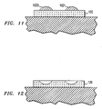
- FIGS. 10-12 schematically show a further embodiment of the inventive method that also can produce a substantial replica.
- a metal e.g., Ce
- uniform-thickness metal bodies 1010 and 1011 remaining on the polyD surface.
- the uniform-thickness bodies are shaped as desired, resulting in template bodies 1020 and 1021.
- FIG. 12 shows the resulting polyD body 120 with non-planar surface, after removal of the "spent" template bodies.
- optical elements e.g., conventional lenticular elements as shown in FIGS. 1-12, or Fresnel lenses
- inventive process is not so limited, and we contemplate manufacture of a wide variety of polyD bodies with one or more non-planar surfaces.
- Such bodies may find use, for instance, for biomedical applications such as prosthetic implants, due to the great inertness of diamond and its high biocompatibility.
- the inventive method is advantageously used for making polyD optical elements.
- diamond including polyD
- powerful refractive optical elements such as lenses can have relatively modest curvature.
- polyD diamond lenses are expected to be far more resistant to damage by high-power laser beams than conventional lenses, due to the strong atomic bonding, very high thermal conductivity and very low thermal expansion coefficient of diamond.
- optical polyD elements including lenses, arrays of lenses and Fresnel lenses
- the non-planar polyD surface will typically be covered with C-containing template material (e.g., Ce-carbide).
- C-containing template material e.g., Ce-carbide
- This "spent" template material can be readily removed by means of, e.g., chemical etching.
- a non-planar surface was created by indentation with a steel sphere (diameter about 1.57 mm), followed by polishing of the surface with emery paper.
- the sheet was placed, non-planar surface down, onto a flat CVD polyD film (about 0.3 mm thick) on an Al2O3 substrate.
- a Mo sheet and a Al2O3 plate were placed between the Ce sheet and a dead weight, the weight providing compressive stress (about 10 psi, corresponding to about 6.9 ⁇ 104 Pa) to the combination.
- the assembly was maintained at about 730°C (i.e., about 60°C below the melting point of Ce) for one week in an Ar atmosphere, followed by cooling to room temperature.
- the above procedure after removal of reacted and/or residual Ce by conventional acid etching, resulted in formation of a non-planar polyD surface that comprised two convex protruding features.
- the shape of the features corresponded substantially to the as-formed indentations in the Ce sheet.
- a Mn plate is formed, by a conventional method, an array of concave indentations (about 0.76 mm radius of curvature, about 0.38 mm deep).
- the resulting non-planar surface is placed onto the planar surface of an as-received CVD polyD film. Intimate contact is attained by means of a dead weight (corresponding to about 100 psi or about 6.9 ⁇ 105 Pa).
- the assembly is maintained for about 100 hours at about 900°C in Ar. After cooling to room temperature, residual Mn is removed by acid etching.
- the resulting non-planar polyD surface comprises an array of convex protruding features that substantially are replicas of the indentations in the Mn plate.
- the non-planar polyD surface is further smoothed by laser planing and mechanical polishing with diamond lapping powder.
- the thus treated polyD film comprises an array of microlenses.
Landscapes
- Physics & Mathematics (AREA)
- Chemical & Material Sciences (AREA)
- Crystallography & Structural Chemistry (AREA)
- General Physics & Mathematics (AREA)
- Optics & Photonics (AREA)
- Engineering & Computer Science (AREA)
- Mechanical Engineering (AREA)
- Crystals, And After-Treatments Of Crystals (AREA)
- Moulds For Moulding Plastics Or The Like (AREA)
Applications Claiming Priority (2)
| Application Number | Priority Date | Filing Date | Title |
|---|---|---|---|
| US3837093A | 1993-03-29 | 1993-03-29 | |
| US38370 | 1993-03-29 |
Publications (1)
| Publication Number | Publication Date |
|---|---|
| EP0618043A1 true EP0618043A1 (de) | 1994-10-05 |
Family
ID=21899551
Family Applications (1)
| Application Number | Title | Priority Date | Filing Date |
|---|---|---|---|
| EP94301902A Withdrawn EP0618043A1 (de) | 1993-03-29 | 1994-03-16 | Gegenstand mit polykristallinem Diamant, und Verfahren zum Formen eines Diamants |
Country Status (3)
| Country | Link |
|---|---|
| US (1) | US5500157A (de) |
| EP (1) | EP0618043A1 (de) |
| JP (1) | JPH06345593A (de) |
Cited By (5)
| Publication number | Priority date | Publication date | Assignee | Title |
|---|---|---|---|---|
| EP0718642A1 (de) * | 1994-12-20 | 1996-06-26 | De Beers Industrial Diamond Division (Proprietary) Limited | Diffraktive Optik |
| EP0739686A3 (de) * | 1995-04-25 | 1996-11-13 | AT&T IPM Corp. | Verfahren und Vorrichtung zum Polieren von metalllöslichen Materialen z.B. Diamant |
| EP0767394A1 (de) * | 1995-10-03 | 1997-04-09 | General Electric Company | Strahlteiler in Form einer optischen Platte aus Diamant |
| WO2004097817A1 (en) * | 2003-04-29 | 2004-11-11 | Koninklijke Philips Electronics N.V. | Optical scanning device and lens therefor |
| WO2006066081A1 (en) * | 2004-12-17 | 2006-06-22 | Eastman Kodak Company | A microlens array |
Families Citing this family (11)
| Publication number | Priority date | Publication date | Assignee | Title |
|---|---|---|---|---|
| US5746931A (en) * | 1996-12-05 | 1998-05-05 | Lucent Technologies Inc. | Method and apparatus for chemical-mechanical polishing of diamond |
| JP2000079636A (ja) * | 1998-07-09 | 2000-03-21 | Canon Inc | 微細加工方法及び装置 |
| US6256149B1 (en) * | 1998-09-28 | 2001-07-03 | Richard W. Rolfe | Lenticular lens sheet and method of making |
| DE10015729B4 (de) * | 2000-03-29 | 2005-09-08 | Fraunhofer-Gesellschaft zur Förderung der angewandten Forschung e.V. | Verfahren zum Herstellen eines Elementes aus polykristallinem Diamant sowie danach hergestelltes Element |
| US7754333B2 (en) * | 2004-09-21 | 2010-07-13 | Smith International, Inc. | Thermally stable diamond polycrystalline diamond constructions |
| US7608333B2 (en) | 2004-09-21 | 2009-10-27 | Smith International, Inc. | Thermally stable diamond polycrystalline diamond constructions |
| US8146744B2 (en) * | 2005-06-10 | 2012-04-03 | Mattel, Inc. | Blister pack assemblies with lenticular lenses |
| US9720133B2 (en) * | 2011-12-16 | 2017-08-01 | Element Six Technologies Limited | Large area optical quality synthetic polycrystalline diamond window |
| US9394747B2 (en) | 2012-06-13 | 2016-07-19 | Varel International Ind., L.P. | PCD cutters with improved strength and thermal stability |
| WO2015193156A1 (en) * | 2014-06-16 | 2015-12-23 | Element Six Technologies Limited | Synthetic diamond optical elements |
| RU2622568C1 (ru) * | 2016-02-02 | 2017-06-16 | Валерий Борисович Дудаков | Способ обработки алмазных кристаллов и алмазных материалов |
Citations (5)
| Publication number | Priority date | Publication date | Assignee | Title |
|---|---|---|---|---|
| GB2061904A (en) * | 1979-04-13 | 1981-05-20 | Inst Geol Yakut Filiala Sibir | Method of processing diamonds |
| JPS6241800A (ja) * | 1985-08-12 | 1987-02-23 | Showa Denko Kk | ダイヤモンド膜の平滑化法 |
| JPH0393695A (ja) * | 1989-09-07 | 1991-04-18 | Sumitomo Electric Ind Ltd | 多結晶ダイヤモンド及びその製造法 |
| JPH0489199A (ja) * | 1990-08-02 | 1992-03-23 | Yamaha Corp | 膜状ダイヤモンド成形体の製造方法 |
| US5240670A (en) * | 1991-08-22 | 1993-08-31 | Texas Instruments Incorporated | Method of improving the mechanical properties of semiconductor materials |
Family Cites Families (3)
| Publication number | Priority date | Publication date | Assignee | Title |
|---|---|---|---|---|
| US4339304A (en) * | 1980-12-30 | 1982-07-13 | Grigoriev Anatoly P | Method of treating diamond |
| US4737248A (en) * | 1985-12-19 | 1988-04-12 | Sumitomo Light Metal Industries, Ltd. | Process for producing dysprosium-iron alloy and neodymium-dysprosium-iron alloy |
| DE3625743A1 (de) * | 1986-07-30 | 1988-02-11 | Winter & Sohn Ernst | Verfahren zum bearbeiten von diamantkoernern |
-
1994
- 1994-03-16 EP EP94301902A patent/EP0618043A1/de not_active Withdrawn
- 1994-03-29 JP JP6057904A patent/JPH06345593A/ja not_active Withdrawn
-
1995
- 1995-01-04 US US08/368,581 patent/US5500157A/en not_active Expired - Lifetime
Patent Citations (5)
| Publication number | Priority date | Publication date | Assignee | Title |
|---|---|---|---|---|
| GB2061904A (en) * | 1979-04-13 | 1981-05-20 | Inst Geol Yakut Filiala Sibir | Method of processing diamonds |
| JPS6241800A (ja) * | 1985-08-12 | 1987-02-23 | Showa Denko Kk | ダイヤモンド膜の平滑化法 |
| JPH0393695A (ja) * | 1989-09-07 | 1991-04-18 | Sumitomo Electric Ind Ltd | 多結晶ダイヤモンド及びその製造法 |
| JPH0489199A (ja) * | 1990-08-02 | 1992-03-23 | Yamaha Corp | 膜状ダイヤモンド成形体の製造方法 |
| US5240670A (en) * | 1991-08-22 | 1993-08-31 | Texas Instruments Incorporated | Method of improving the mechanical properties of semiconductor materials |
Non-Patent Citations (3)
| Title |
|---|
| DATABASE WPI Section Ch Week 9122, Derwent World Patents Index; Class EJL, AN 91-159309 C22! * |
| PATENT ABSTRACTS OF JAPAN vol. 11, no. 229 (C - 436) 25 July 1987 (1987-07-25) * |
| PATENT ABSTRACTS OF JAPAN vol. 16, no. 314 (M - 1278) 9 July 1992 (1992-07-09) * |
Cited By (6)
| Publication number | Priority date | Publication date | Assignee | Title |
|---|---|---|---|---|
| EP0718642A1 (de) * | 1994-12-20 | 1996-06-26 | De Beers Industrial Diamond Division (Proprietary) Limited | Diffraktive Optik |
| EP0739686A3 (de) * | 1995-04-25 | 1996-11-13 | AT&T IPM Corp. | Verfahren und Vorrichtung zum Polieren von metalllöslichen Materialen z.B. Diamant |
| US5846122A (en) * | 1995-04-25 | 1998-12-08 | Lucent Technologies Inc. | Method and apparatus for polishing metal-soluble materials such as diamond |
| EP0767394A1 (de) * | 1995-10-03 | 1997-04-09 | General Electric Company | Strahlteiler in Form einer optischen Platte aus Diamant |
| WO2004097817A1 (en) * | 2003-04-29 | 2004-11-11 | Koninklijke Philips Electronics N.V. | Optical scanning device and lens therefor |
| WO2006066081A1 (en) * | 2004-12-17 | 2006-06-22 | Eastman Kodak Company | A microlens array |
Also Published As
| Publication number | Publication date |
|---|---|
| JPH06345593A (ja) | 1994-12-20 |
| US5500157A (en) | 1996-03-19 |
Similar Documents
| Publication | Publication Date | Title |
|---|---|---|
| US5500157A (en) | Method of shaping polycrystalline diamond | |
| US5154023A (en) | Polishing process for refractory materials | |
| CA2177345C (en) | Method for the growth of industrial crystals | |
| KR100212120B1 (ko) | Cvd다이아몬드 공작편의 제조방법 | |
| EP1483782B1 (de) | Herstellungsverfahren für eine sic-monitor-wafer | |
| KR102473088B1 (ko) | 탄화규소 기판의 제조 방법 및 탄화규소 기판 | |
| EP2719794A2 (de) | Plasmaätzen von Diamantoberflächen | |
| US20030019843A1 (en) | Ceramic member with fine protrusions on surface and method of producing the same | |
| EP0671482A1 (de) | Gehärteter, aus der Dampfphase chemisch abgeschiedener Diamant | |
| EP0645478B1 (de) | Verfahren zum Formen eines Diamantkörpers | |
| US4604292A (en) | X-ray mask blank process | |
| JP3273921B2 (ja) | ガラス光学素子用成形型、ガラス光学素子の製造方法および成形型の再生方法 | |
| CN109136920B (zh) | 一种基于非晶合金的铍镜镜面层及其制备方法 | |
| US5665252A (en) | Method of shaping a polycrystalline diamond body | |
| EP0590871A1 (de) | Ätzen eines Diamantenkörpers mit Hilfe von geschmolzenen Legierungen die seltene Erden enthalten | |
| KR102523181B1 (ko) | 플렉서블 시트 상에 막을 제조하는 방법 | |
| Jin et al. | Thinning and patterning of CVD diamond films by diffusional reaction | |
| JP4711242B2 (ja) | 複合構造物およびその作製方法 | |
| JPH1171197A (ja) | 表面強化ダイヤモンド及びその製造方法 | |
| JP4942131B2 (ja) | スタンパ及びそれを用いたナノ構造の転写方法 | |
| JP2649582B2 (ja) | SiCコーテイングSiCセラミックスの製造方法 | |
| JP2002348129A (ja) | ガラス光学素子成型金型の製造方法及びガラス光学素子の成形方法 | |
| US20260071317A1 (en) | Composite of a substrate coated with a mechanically interlocked coating, cutting element and method for depositing a mechanically interlocked coating upon a substrate | |
| JP3046184B2 (ja) | ガラス光学素子の製造方法 | |
| JPH09286624A (ja) | 光学素子成形用型 |
Legal Events
| Date | Code | Title | Description |
|---|---|---|---|
| PUAI | Public reference made under article 153(3) epc to a published international application that has entered the european phase |
Free format text: ORIGINAL CODE: 0009012 |
|
| AK | Designated contracting states |
Kind code of ref document: A1 Designated state(s): DE FR GB |
|
| 17P | Request for examination filed |
Effective date: 19950323 |
|
| 17Q | First examination report despatched |
Effective date: 19960125 |
|
| STAA | Information on the status of an ep patent application or granted ep patent |
Free format text: STATUS: THE APPLICATION IS DEEMED TO BE WITHDRAWN |
|
| 18D | Application deemed to be withdrawn |
Effective date: 19970607 |