EP0618576A2 - Système de modulation et démodulation de données digitales - Google Patents
Système de modulation et démodulation de données digitales Download PDFInfo
- Publication number
- EP0618576A2 EP0618576A2 EP94302362A EP94302362A EP0618576A2 EP 0618576 A2 EP0618576 A2 EP 0618576A2 EP 94302362 A EP94302362 A EP 94302362A EP 94302362 A EP94302362 A EP 94302362A EP 0618576 A2 EP0618576 A2 EP 0618576A2
- Authority
- EP
- European Patent Office
- Prior art keywords
- code
- bit
- word
- modulated
- words
- Prior art date
- Legal status (The legal status is an assumption and is not a legal conclusion. Google has not performed a legal analysis and makes no representation as to the accuracy of the status listed.)
- Withdrawn
Links
Images





Classifications
-
- G—PHYSICS
- G11—INFORMATION STORAGE
- G11B—INFORMATION STORAGE BASED ON RELATIVE MOVEMENT BETWEEN RECORD CARRIER AND TRANSDUCER
- G11B20/00—Signal processing not specific to the method of recording or reproducing; Circuits therefor
- G11B20/10—Digital recording or reproducing
- G11B20/14—Digital recording or reproducing using self-clocking codes
- G11B20/1403—Digital recording or reproducing using self-clocking codes characterised by the use of two levels
- G11B20/1423—Code representation depending on subsequent bits, e.g. delay modulation, double density code, Miller code
- G11B20/1426—Code representation depending on subsequent bits, e.g. delay modulation, double density code, Miller code conversion to or from block codes or representations thereof
-
- H—ELECTRICITY
- H03—ELECTRONIC CIRCUITRY
- H03M—CODING; DECODING; CODE CONVERSION IN GENERAL
- H03M5/00—Conversion of the form of the representation of individual digits
- H03M5/02—Conversion to or from representation by pulses
- H03M5/04—Conversion to or from representation by pulses the pulses having two levels
- H03M5/14—Code representation, e.g. transition, for a given bit cell depending on the information in one or more adjacent bit cells, e.g. delay modulation code, double density code
- H03M5/145—Conversion to or from block codes or representations thereof
Definitions
- the present invention generally relates to a digital data modulation/demodulation system, and more particularly to a modulator/demodulator which is used for digital data recording/reproducing to/from optical discs etc., or communication transmission.
- EFM Eight-to-Fourteen Modulation
- CD Compact Disc
- RLL Run-Length Limited two-to-seven
- modulated codes after conversion such characteristic parameters as a bit interval T, a minimum inversion interval Tmin, a maximum inversion interval Tmax, a detection window width Tw, a digital sum value DSV, etc., have been established.
- a bit interval T a minimum inversion interval Tmin, a maximum inversion interval Tmax, a detection window width Tw, a digital sum value DSV, etc.
- the minimum inversion interval Tmin is the most important parameter as it directly affects the shortest bit length that can be reconstructed on an optical disc.
- a shortest writable or readable bit length on a disc is determined by an attribute of the light source, i.e., a wavelength of a laser beam generated from an optical head for writing or reading optical data on a disc, as well as a numerical aperture NA of an optical objective lens to minimize a light spot diameter as small as possible, etc. Therefore, in order to make the bit length more short and increase a recording density, it is needed to develop a laser with short wavelength beam and expand the numerical aperture NA, but it was difficult to limit a writable disc bit length to below a fixed value as it was difficult to use them in practical use.
- an object of the present invention to provide digital data modulation/demodulation system which is able to realize a large capacity optical disc by removing the defects as described above for achieving higher density recording of data using currently available optical systems.
- a digital data modulation/demodulation system includes a separator for separating a consecutive binary data sequence into every four-bit code-words, a four-to-nine (hereinafter referred to as [4,9]) converter using variable length words for converting the separated four-bit code-words into nine-bit modulated code-words having three consecutive bits of "0" and a code selecting means for selecting a modulated code-word among nine-bit code-words having minimum three bits of "0" between a first bit of "1” and a following second bit of "1", so that there should not be less than two consecutive bits of "0" between a preceding and succeeding modulated code-words.
- bits are so controlled by a code selecting means that less than two consecutive bits of "0" are not generated between a current modulated code-word and a modulated code-word to be converted next.
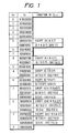
- FIGURE 1 is an explanatory diagram of a code conversion table showing an embodiment of the present invention.
- Dn shows an input binary data sequence separated in four bit code-words and expressed in the hexadecimal notation.
- Tn shows a binary bit pattern after converting the input Dn into nine-bit data. Only Tn having minimum three bits of "0" between a preceding bit "1” and a succeeding bit "1" has been selected.
- Tn pattern for a balance with a succeeding data (Dn+1) and Tn pattern is specified according to a value of Dn+1.
- Dn+1 5
- Tn+1 6
- D, or F data is converted into "000010001” andin other cases, itis converted into "000000100”.
- 000010001 is selected as Tn
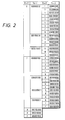
- data is converted according to a conversion table shown in FIGURE 2 for Dn+1 and further, including a Dn+2 succeeding to it in some cases.
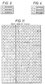
- Tn+1 is specified according to a table shown in FIGURE 4. This is because the number of bits "0" can be reduced when compared with a case using the table shown in FIGURE 3 and if maximum inversion interval Tmax is not a problem, there will be no problem even when the conversion is made according to the table shown in FIGURE 3.
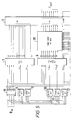
- FIGURE 5 is a circuit block diagram of an encoder to realize the conversion tables shown in FIGURES 1 through 4.
- outputs S0, S1 of a selector controller 1 show "0" and a selector (SEL) 2 selects DO input, accordingly.
- the output of a first conversion logic circuit, that is, the output of the TLGC(a) 3 is input directly to the selector 2.
- the output of a second conversion logic circuit in the same construction as the first conversion logic circuit, that is, the TLGC(b) is input to the selector 2 via a three-input OR gate 18.
- the specified construction of the three-input OR gate block 18 is shown in FIGURE 6.
- a truth table of the TLGC(a) 3 is shown in FIGURE 7. Whether a value of four-bit code-word (Dn+1) to be input next is 6, 7, 8, D, F or 0, 9, A is judged from the output SL1 of DET 4 and the output SL2 of DET 5.
- the next code-word Dn+1 is converted by one of the conversion logic circuits TLGC(b) 6 for (6, 7), TLGC(c) 7 for (8, D, F) or TLGC(d) 8 for (0, 9, A).
- the outputs of the TLGC(b) 6, TLGC(c) 7 and TLGC(d) 8 are input to the three-input OR gate 18, respectively and select prescribed conversion outputs.
- Truth tables of the TLGC(b) 6, TLGC(c) 7 and TLGC(d) 8 are shown in FIGURES 8, 9 and 10, respectively.
- Tn, Tn+1 and Tn+2 are decided by the second conversion logic circuit TLGC(b) 6 based on the outputs SL3, SL4 and SL5 of the DET 10 for (B, C, D, E), the DET 11 for (5, 8, A) and the DET 12 for (6, 7, F) for judging its value including a value of the succeeding Dn+2 in addition to the output of a data latch 15.
- a succeeding code-word Dn+2 is converted by the TLGC(e) 13.
- whether a preceding code-word Dn+1 is 7 or 6 is detected by (7) DET 14 and the corresponding conversion to the data Tn+2 is made according to the table shown in FIGURE 2.
- a truth table of the TLGC(e) 13 is shown in FIGURE 11.
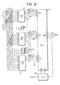
- FIGURE 12 shows a circuit block diagram of a decoder to realize the conversion tables shown in FIGURES 1 through 4.
- a selector controller 100 operates in the entirely same manner as the selector control circuit 1 of the encoder. That is, both the outputs S0 and S1 of the selector control circuit 100 under the initial state show "0" and the selector (SEL2) 19 selects the D0 input, correspondingly.
- the first process of encoded data Tn is carried out by a conversion logic circuit TLGC(f) 20 and restoration handling data Dn including the output SF1 showing whether the data Tn+1 successively input is restricted and the output SL1 showing that the data Tn+1 is one of 0, 6, 7, 8, 9, A, D and F is output.
- This TLGC(g) 21 further outputs a restoration handling data Dn including an output SF2 showing whether the data Tn+2 successively input is restricted, an output SL2 showing that the data is one of B, C, D, and E, an output SL3 showing that the data is one of 5, 8 and A, and an output SL4 showing that the data is one of 6, 7 and F.
- the decoder processes the restoration while judging whether the decoding of a received code-word is completed.
- SYNC code, etc. are generally inserted at a fixed interval as a measure when any error is generated and therefore, there is no problem.
- DC control code 25 is available in two kinds: "010001000” and "000001000", and a pattern for making DSV smaller is selected and inserted. To be concrete, for DC control code 25 to be inserted after (m)-series data, a pattern for making DSV smaller is finally selected by calculating DSV up to the next (m+1)-series data.
- FIGURES 19 and 20 the result of comparison test of the [4,9] modulation system of the present invention with the conventional EFM modulation system conducted based on the embodiment described above is shown in FIGURES 19 and 20.
- the eye pattern (FIGURE 20) of the reproduced signal according to the [4,9] modulation system of the present invention has an amplitude larger than the eye pattern (FIGURE 19) according to the conventional EFM modulation system and it is therefore expected that read errors will be reduced extremely.
- FIGURES 1 through 4 One embodiment of the present invention has been described above with reference to the drawings.
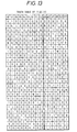
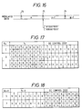
- the present invention is not limited to the tables shown in FIGURES 1 through 4, FIGURES 7 thtough 11, FIGURES 13 through 15, and FIGURES 17 and 18.
- a code length was restricted to maximum three codes in some cases but there will be no problem even when it is extended to four codes or limited to less than two codes.
- according to the present invention can provide an extremely preferable digitl data modulation/demodulation sustem, which is able to prevent the generation of a state containing less than 3 continuous bits "0" between modulated code-words to be continuously converted, it is possible to make the minimum inversion interval Tmin large, thus realizing a large capacity optical disc with improved recording density.
Landscapes
- Engineering & Computer Science (AREA)
- Theoretical Computer Science (AREA)
- Signal Processing (AREA)
- Signal Processing For Digital Recording And Reproducing (AREA)
- Dc Digital Transmission (AREA)
Applications Claiming Priority (4)
| Application Number | Priority Date | Filing Date | Title |
|---|---|---|---|
| JP76692/93 | 1993-04-02 | ||
| JP7669293 | 1993-04-02 | ||
| JP48429/94 | 1994-03-18 | ||
| JP6048429A JPH0730431A (ja) | 1993-04-02 | 1994-03-18 | データ変復調方式および変復調装置 |
Publications (2)
| Publication Number | Publication Date |
|---|---|
| EP0618576A2 true EP0618576A2 (fr) | 1994-10-05 |
| EP0618576A3 EP0618576A3 (fr) | 1996-07-03 |
Family
ID=26388701
Family Applications (1)
| Application Number | Title | Priority Date | Filing Date |
|---|---|---|---|
| EP94302362A Withdrawn EP0618576A3 (fr) | 1993-04-02 | 1994-03-31 | Système de modulation et démodulation de données digitales. |
Country Status (5)
| Country | Link |
|---|---|
| US (1) | US5579003A (fr) |
| EP (1) | EP0618576A3 (fr) |
| JP (1) | JPH0730431A (fr) |
| KR (1) | KR0136715B1 (fr) |
| TW (1) | TW239240B (fr) |
Families Citing this family (13)
| Publication number | Priority date | Publication date | Assignee | Title |
|---|---|---|---|---|
| JP2920065B2 (ja) * | 1994-03-16 | 1999-07-19 | 株式会社東芝 | データ記録方法、記録装置、再生装置及び再生方法 |
| JP2786810B2 (ja) * | 1994-03-16 | 1998-08-13 | 株式会社東芝 | 光ディスクおよびその信号記録装置ならびに信号再生装置 |
| JP2944895B2 (ja) * | 1994-09-02 | 1999-09-06 | 株式会社日立製作所 | 情報再生装置及び情報記録方法 |
| KR0183722B1 (ko) * | 1995-07-20 | 1999-04-15 | 김광호 | 디지탈 신호 변조부호기 및 복호기 |
| JP3521050B2 (ja) | 1997-01-28 | 2004-04-19 | 株式会社東海理化電機製作所 | 操作装置 |
| KR100257538B1 (ko) * | 1997-07-14 | 2000-06-01 | 구자홍 | 복사 방지용 광디스크의 신호 기록방법 및 이 기록방법을 이용한 광디스크의 복제방지방법 |
| US6222524B1 (en) | 1997-08-25 | 2001-04-24 | International Business Machines Corporation | Mouth operated input device for an electronically responsive device |
| TW565829B (en) * | 2002-03-19 | 2003-12-11 | Via Tech Inc | Method and device for recovering decoded data |
| JP4391193B2 (ja) | 2003-03-27 | 2009-12-24 | 本田技研工業株式会社 | 操作装置 |
| JP4359478B2 (ja) | 2003-10-14 | 2009-11-04 | アルプス電気株式会社 | ジョイスティック型スイッチ装置 |
| DE602004010763T2 (de) | 2003-10-14 | 2008-04-30 | Alps Electric Co., Ltd. | Steuerknüppeleingabegerät |
| JP4930760B2 (ja) * | 2006-04-28 | 2012-05-16 | ソニー株式会社 | 変調装置および方法、並びに記録媒体 |
| JP4899616B2 (ja) * | 2006-04-28 | 2012-03-21 | ソニー株式会社 | 変調装置および方法、プログラム、並びに記録媒体 |
Family Cites Families (9)
| Publication number | Priority date | Publication date | Assignee | Title |
|---|---|---|---|---|
| US3685033A (en) * | 1970-08-24 | 1972-08-15 | Honeywell Inc | Block encoding for magnetic recording systems |
| US3689899A (en) * | 1971-06-07 | 1972-09-05 | Ibm | Run-length-limited variable-length coding with error propagation limitation |
| NL186790C (nl) * | 1980-07-14 | 1991-02-18 | Philips Nv | Werkwijze voor het coderen van een reeks van blokken tweetallige databits in een reeks van blokken van tweetallige kanaalbits, alsmede modulator, demodulator en registratiedrager te gebruiken bij de werkwijze. |
| US4544962A (en) * | 1981-07-06 | 1985-10-01 | Matsushita Electric Industrial Co., Ltd. | Method and apparatus for processing binary data |
| JPS58220211A (ja) * | 1982-06-16 | 1983-12-21 | Matsushita Electric Ind Co Ltd | デイジタル変調方法 |
| US4833470A (en) * | 1986-07-15 | 1989-05-23 | Matsushita Electric Industrial Co., Ltd. | Code conversion apparatus |
| JP3071500B2 (ja) * | 1991-07-11 | 2000-07-31 | チノン株式会社 | ズームカメラのファインダ装置 |
| JPH05234279A (ja) * | 1992-02-24 | 1993-09-10 | Sony Corp | 最尤復号装置及びこれを用いた再生データ復調装置 |
| TW219416B (fr) * | 1992-03-10 | 1994-01-21 | Sony Co Ltd |
-
1994
- 1994-03-18 JP JP6048429A patent/JPH0730431A/ja active Pending
- 1994-03-31 EP EP94302362A patent/EP0618576A3/fr not_active Withdrawn
- 1994-04-01 US US08/221,956 patent/US5579003A/en not_active Expired - Fee Related
- 1994-04-01 KR KR1019940006883A patent/KR0136715B1/ko not_active Expired - Fee Related
- 1994-04-07 TW TW083103008A patent/TW239240B/zh active
Also Published As
| Publication number | Publication date |
|---|---|
| KR0136715B1 (ko) | 1998-05-15 |
| JPH0730431A (ja) | 1995-01-31 |
| TW239240B (fr) | 1995-01-21 |
| US5579003A (en) | 1996-11-26 |
| EP0618576A3 (fr) | 1996-07-03 |
Similar Documents
| Publication | Publication Date | Title |
|---|---|---|
| US5774078A (en) | Single merging bit DC-suppressed run length limited coding | |
| KR100263689B1 (ko) | 변조방법, 변조장치 및 복조장치 | |
| EP0618576A2 (fr) | Système de modulation et démodulation de données digitales | |
| EP0691750B1 (fr) | Procédé pour la modulation ou démodulation numérique et appareil pour utiliser cette modulation ou démodulation | |
| EP1431972A2 (fr) | Méthode et appareil de modulation de code, méthode et appareil de démodulation et support d'enregistrement d'information | |
| US7750828B2 (en) | Systems and methods for encoding and decoding data using selective substitution of conversion table | |
| US6058087A (en) | Information recording apparatus, information recording medium and information reproducing apparatus | |
| EP1494235A1 (fr) | Support, procede et dispositif d'enregistrement de donnees | |
| KR20000035065A (ko) | 데이터 변/복조방법과 이를 이용한 변/복조 장치 및 그 기록매체 | |
| JPH11177432A (ja) | 変調装置および方法、並びに提供媒体 | |
| US7016287B2 (en) | Method and apparatus of modulating/demodulating data for an optical recording medium | |
| GB2078061A (en) | Method of encoding data bits on a record carrier device for carrying out the method record carrier provided with an information structure and device for decoding the signal read from the record carrier | |
| US6670896B2 (en) | Method and apparatus for modulating and demodulating digital data | |
| US6172622B1 (en) | Demodulating device, demodulating method and supply medium | |
| US6898166B2 (en) | Synchronous signal generating method, recording apparatus, transmitting apparatus, recording medium, and transmission medium | |
| JP3013651B2 (ja) | デジタル変調装置 | |
| JPH0363859B2 (fr) | ||
| US7167524B2 (en) | Method of inserting sync data in modulated data and recording medium containing the sync data | |
| JP4027774B2 (ja) | 情報記録装置及び情報再生装置 | |
| NL1016579C2 (nl) | Werkwijze voor het vervaardigen van een registratiedrager alsmede een dergelijke registratiedrager. | |
| KR100224816B1 (ko) | 디지탈 데이터의 변조방법 | |
| KR850000953B1 (ko) | 2진 데이타비트 블럭열을 2진 채널비트 블럭열로 코딩시키는 방법 | |
| KR100224817B1 (ko) | 디지탈 데이터의 변조방법 | |
| KR0144965B1 (ko) | 이.에프.엠.(efm)복조의 에러정정방법 | |
| US20070115155A1 (en) | Demodulation table, demodulating device and demodulating method, program, and recording medium |
Legal Events
| Date | Code | Title | Description |
|---|---|---|---|
| PUAI | Public reference made under article 153(3) epc to a published international application that has entered the european phase |
Free format text: ORIGINAL CODE: 0009012 |
|
| 17P | Request for examination filed |
Effective date: 19940426 |
|
| AK | Designated contracting states |
Kind code of ref document: A2 Designated state(s): AT BE CH DE DK ES FR GB GR IE IT LI LU MC NL PT SE |
|
| RAX | Requested extension states of the european patent have changed |
Free format text: SI PAYMENT 940426 |
|
| PUAL | Search report despatched |
Free format text: ORIGINAL CODE: 0009013 |
|
| AK | Designated contracting states |
Kind code of ref document: A3 Designated state(s): AT BE CH DE DK ES FR GB GR IE IT LI LU MC NL PT SE |
|
| AX | Request for extension of the european patent |
Free format text: SI PAYMENT 940426 |
|
| 17Q | First examination report despatched |
Effective date: 19970523 |
|
| STAA | Information on the status of an ep patent application or granted ep patent |
Free format text: STATUS: THE APPLICATION IS DEEMED TO BE WITHDRAWN |
|
| 18D | Application deemed to be withdrawn |
Effective date: 19971203 |