EP0618651A2 - Oberflächenemittierender Laser mit Lichtmodulator - Google Patents
Oberflächenemittierender Laser mit Lichtmodulator Download PDFInfo
- Publication number
- EP0618651A2 EP0618651A2 EP94101206A EP94101206A EP0618651A2 EP 0618651 A2 EP0618651 A2 EP 0618651A2 EP 94101206 A EP94101206 A EP 94101206A EP 94101206 A EP94101206 A EP 94101206A EP 0618651 A2 EP0618651 A2 EP 0618651A2
- Authority
- EP
- European Patent Office
- Prior art keywords
- layer
- quantum well
- surface emitting
- emitting laser
- bragg reflector
- Prior art date
- Legal status (The legal status is an assumption and is not a legal conclusion. Google has not performed a legal analysis and makes no representation as to the accuracy of the status listed.)
- Withdrawn
Links
Images



Classifications
-
- H—ELECTRICITY
- H01—ELECTRIC ELEMENTS
- H01S—DEVICES USING THE PROCESS OF LIGHT AMPLIFICATION BY STIMULATED EMISSION OF RADIATION [LASER] TO AMPLIFY OR GENERATE LIGHT; DEVICES USING STIMULATED EMISSION OF ELECTROMAGNETIC RADIATION IN WAVE RANGES OTHER THAN OPTICAL
- H01S5/00—Semiconductor lasers
- H01S5/10—Construction or shape of the optical resonator, e.g. extended or external cavity, coupled cavities, bent-guide, varying width, thickness or composition of the active region
- H01S5/18—Surface-emitting [SE] lasers, e.g. having both horizontal and vertical cavities
- H01S5/183—Surface-emitting [SE] lasers, e.g. having both horizontal and vertical cavities having only vertical cavities, e.g. vertical cavity surface-emitting lasers [VCSEL]
- H01S5/18341—Intra-cavity contacts
-
- H—ELECTRICITY
- H01—ELECTRIC ELEMENTS
- H01S—DEVICES USING THE PROCESS OF LIGHT AMPLIFICATION BY STIMULATED EMISSION OF RADIATION [LASER] TO AMPLIFY OR GENERATE LIGHT; DEVICES USING STIMULATED EMISSION OF ELECTROMAGNETIC RADIATION IN WAVE RANGES OTHER THAN OPTICAL
- H01S3/00—Lasers, i.e. devices using stimulated emission of electromagnetic radiation in the infrared, visible or ultraviolet wave range
- H01S3/10—Controlling the intensity, frequency, phase, polarisation or direction of the emitted radiation, e.g. switching, gating, modulating or demodulating
- H01S3/105—Controlling the intensity, frequency, phase, polarisation or direction of the emitted radiation, e.g. switching, gating, modulating or demodulating by controlling the mutual position or the reflecting properties of the reflectors of the cavity, e.g. by controlling the cavity length
- H01S3/1055—Controlling the intensity, frequency, phase, polarisation or direction of the emitted radiation, e.g. switching, gating, modulating or demodulating by controlling the mutual position or the reflecting properties of the reflectors of the cavity, e.g. by controlling the cavity length one of the reflectors being constituted by a diffraction grating
-
- H—ELECTRICITY
- H01—ELECTRIC ELEMENTS
- H01S—DEVICES USING THE PROCESS OF LIGHT AMPLIFICATION BY STIMULATED EMISSION OF RADIATION [LASER] TO AMPLIFY OR GENERATE LIGHT; DEVICES USING STIMULATED EMISSION OF ELECTROMAGNETIC RADIATION IN WAVE RANGES OTHER THAN OPTICAL
- H01S5/00—Semiconductor lasers
- H01S5/06—Arrangements for controlling the laser output parameters, e.g. by operating on the active medium
- H01S5/0607—Arrangements for controlling the laser output parameters, e.g. by operating on the active medium by varying physical parameters other than the potential of the electrodes, e.g. by an electric or magnetic field, mechanical deformation, pressure, light, temperature
- H01S5/0614—Arrangements for controlling the laser output parameters, e.g. by operating on the active medium by varying physical parameters other than the potential of the electrodes, e.g. by an electric or magnetic field, mechanical deformation, pressure, light, temperature controlled by electric field, i.e. whereby an additional electric field is used to tune the bandgap, e.g. using the Stark-effect
-
- H—ELECTRICITY
- H01—ELECTRIC ELEMENTS
- H01S—DEVICES USING THE PROCESS OF LIGHT AMPLIFICATION BY STIMULATED EMISSION OF RADIATION [LASER] TO AMPLIFY OR GENERATE LIGHT; DEVICES USING STIMULATED EMISSION OF ELECTROMAGNETIC RADIATION IN WAVE RANGES OTHER THAN OPTICAL
- H01S5/00—Semiconductor lasers
- H01S5/10—Construction or shape of the optical resonator, e.g. extended or external cavity, coupled cavities, bent-guide, varying width, thickness or composition of the active region
- H01S5/18—Surface-emitting [SE] lasers, e.g. having both horizontal and vertical cavities
- H01S5/183—Surface-emitting [SE] lasers, e.g. having both horizontal and vertical cavities having only vertical cavities, e.g. vertical cavity surface-emitting lasers [VCSEL]
- H01S5/18302—Surface-emitting [SE] lasers, e.g. having both horizontal and vertical cavities having only vertical cavities, e.g. vertical cavity surface-emitting lasers [VCSEL] comprising an integrated optical modulator
Definitions
- the present invention relates to a surface emitting laser provided with a light modulator.
- an external modulator for changing the light intensity of a semiconductor laser one is known which is made by forming an n-InP cladding layer 2, InGaAsP quantum well layer 3, and p-InP cladding layer 4 on an n-InP substrate 1 in order by means of epitaxial growth and forming a p-electrode 5 on the cladding layer 4 and an n-electrode 6 under the substrate 1 as shown in Fig. 1A.
- the external light modulator changes the absorption wavelength of the light passing through the quantum well layer 3 to perform light modulation by using the characteristic that the light absorption coefficient of the quantum well layer 3 is changed due to a change of the electric field in the quantum well layer 3.
- n-InP buffer layer 8 saturable absorption layer 9 comprising an n-InGaAs/InP superlattice, n-InP cladding layer 10, active layer 11 comprising an InGaAs/InP superlattice, p-InP cladding layer 12, and p-InGaAs cap layer 13 are formed on an n-InP substrate 7 in order, high-reflectance films 14 and 15 are formed on the cap layer 13 and under the semiconductor substrate 7, a p-electrode 16 is formed around the high-reflectance film 14 on the cap layer 13, an n-electrode 17 is formed on the outer periphery of the saturable absorption layer 9, and moreover an electrode 18 for applying an electric field to the saturable absorption layer 9 is
- This apparatus changes the quantity of light to be absorbed in a resonator by the saturable absorption layer 9 to perform light modulation by using the characteristic that a light absorption wavelength is changed due to the quantum-confinement Stark effect when applying an electric field to the saturable absorption layer 9.
- Embodiments of the present invention may provide a surface emitting laser for accurately controlling an absorption wavelength without being subject to the current flowing through a resonator.
- One embodiment provides a surface emitting laser having a quantum well structure in which a light absorption wavelength band is changed due to the presence and absence of an electric field, which is provided in a non-doped Distributed Bragg Reflector mirror at the opposite side to a semiconductor substrate.
- a change of the light absorption wavelength band is caused by the Wannier-Stark effect or quantum-confinement Stark effect.
- the modulator is not subject to the current flowing through the resonator and securely controls the optical output because the quantum well structure is formed not in the resonator but in the DBR mirror outside the resonator.
- another embodiment of the present invention provides a surface emitting laser in which a multiple quantum well layer is formed where a light absorption wavelength band includes a laser oscillation wavelength when no electric field is applied to the non-doped DBR mirror at the opposite side to a substrate out of two non-doped DBR mirror formed at the both ends of a resonator but does not include the laser oscillation wavelength when an electric field is applied to it.
- the change of a light absorption wavelength edge due to the presence and absence of an electric field is caused by the Wannier-Stark effect. That is, when an electric field is applied, the light absorption loss is small in a low refractive index layer of one DBR mirror, the reflectance of the DBR mirror increases, laser oscillation is obtained at a low threshold, and light is effectively output. When no electric field is applied, light absorption in the low refractive index layer extremely increases and the reflectance of a DBR mirror decreases. Therefore, the reflection loss of the resonator greatly increases and, at the same time, the light outputting efficiency is decreased due to the increase of light absorption and the optical output decreases.
- the light output of a surface emitting laser is modulated by intermittently applying an electric field.
- Still another embodiment of the present invention provides a surface emitting laser in which a quantum well structure with an energy band gap larger than that of an active layer is provided in a low refractive index layer of the DBR mirror at the opposite side to a substrate out of a pair of non-doped DBR mirrors formed at the both ends of a resonator.
- the light absorption loss is small because the energy band gap of the quantum well in the DBR mirror is larger than that of an active layer.
- the energy band gap of the quantum well in the DBR mirror gets small by quantum-confinement Stark effect and light absorption extremely increases.
- the wavelength where the reflectivity of the DBR mirror is maximized changes.
- a quantum well structure in which a light absorption wavelength is changed by applying an electric field is provided in a non-doped DBR mirror formed at an end of a resonator. Therefore, it is possible to accurately control an absorption wavelength without being subject to the current flowing through the resonator.
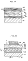
- Figs. 2A and 2B are sectional views of the steps of fabricating the surface emitting laser of the first embodiment of the present invention
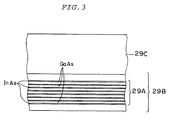
- Fig. 3 is a partially sectional view of a DBR mirror of the surface emitting laser
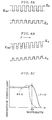
- Figs. 4A to 4C are illustrations for explaining operations of the surface emitting laser.
- the surface emitting laser has a structure in which the oscillation wavelength ⁇ 0 equals 0.98 ⁇ m.
- a lower Distributed Bragg Reflector mirror (DBR) 22 comprising 28.5 pairs of an n-AlAs layer and an n-GaAs layer is formed by forming an n-AlAs layer up to the thickness of 83.1 nm and an n-GaAs layer up to the thickness of 69.6 nm, in order, by means of the metal-organic chemical vapor deposition on an n-GaAs substrate 21 with the Si concentration of 2 x 10¹⁸atoms/cm3 and the thickness of 100 ⁇ m and repeating the formation of the layers.
- the Si concentration of the n-AlAs layer and n-GaAs layer is 3 x 10¹⁸atoms/cm3 respectively and the n-AlAs layer pairs with the n-GaAs layer.
- the total thickness from the n-Al 0.2 Ga 0.8 As cladding layer 23 to the top first p-GaAs contact layer 28 comes to a value integer (N) times as long as the half-wavelength ⁇ /2 and the distance from the bottom of the n-Al 0.2 Ga 0.8 As cladding layer 23 to a center of the thickness of the single quantum well active layer 25 in the film thickness direction comes to a value integer (M) (M ⁇ N) times as long as the half-wavelength ⁇ /2.
- M integer (M ⁇ N) times as long as the half-wavelength ⁇ /2.
- an AlAs layer 29C makes a pair with two GaAs layers 29B which sandwich a superlattice structure (also known as a multiple quantum well structure) 29A made by alternately and repeatedly depositing a 1-atom InAs layer and a 4-atom GaAs layer 20 times and the paired layers are repeatedly deposited up to 23 stages to constitute an upper DBR mirror 29.
- a superlattice structure also known as a multiple quantum well structure
- the total thickness of the superlattice structure 29A and the GaAs layer under the structure 29A is set to 70 nm
- the total thickness of the two GaAs layers 29B sandwiching the superlattice structure 29A is set to 48.6 nm
- the thickness of the AlAs layer 29C is set to 83.1 nm.
- the superlattice structure 29A and the GaAs layers 29B serve as a high refractive index layer
- the AlAs layer 29C serves as a low refractive index layer.
- the upper DBR mirror 29 is formed as a non-doped layer containing no impurity.
- a second p-GaAs contact layer 30 with the Zn concentration of 3 x 10¹⁸atoms/cm3 is formed up to the thickness of 500 nm as shown in Fig. 2A.
- the second p-GaAs contact layer 30 and the upper DBR mirror 29 are patterned by means of dry etching such as RIBE (Reactive Ion Beam Etching) using a chlorine-based gas by using a not-illustrated SiO2 pattern as a mask.
- RIBE Reactive Ion Beam Etching
- a three-layer metallic film formed by depositing Ti, Pt, and Au in order is deposited on the contact layer 30 on the upper DBR mirror 29 and on the p-GaAs contact layer 28 around the mirror 29 by means of sputtering.
- the metallic film on the DBR mirror 29 is used as a light modulation electrode 31 and the metallic film on the contact layer 28 is used as a p-electrode 32.
- n-electrode 33 formed by depositing AuGe and Au in order and having a light passing hole 34 at its center is formed at the bottom of the GaAs substrate 21 just under the patterned upper DBR mirror 29.
- Light modulation of the surface emitting laser is performed by applying a predetermined signal for electric field modulation to the light modulation electrode 31 and modulating the output light of the surface emitting laser.
- the theory of the modulation is described below.
- light with the oscillation wavelength of ⁇ 0 of the surface emitting laser is modulated by applying a modulation signal to the DBR mirror 29 at the opposite side to the semiconductor substrate 21.
- this embodiment has a structure for absorbing the light by making the light absorption wavelength edge longer than the oscillation wavelength ⁇ 0 of the laser when no electric field is applied to the superlattice structure 29A in the upper DBR mirror 29 shown in Fig. 2B and passing the light by making the light absorption wavelength edge shorter than the oscillation wavelength ⁇ 0 of the laser when an electric field is applied.
- the reflectivity of the upper DBR mirror 29 increases, a low-threshold laser oscillation is obtained, and light is effectively emitted when an electric field is applied.
- the light absorption coefficient of the DBR mirror 29 extremely increases. Therefore, the reflectivity of the DBR mirror 29 decreases, the reflection loss of the resonator greatly increases, and at the same time, the light outputting efficiency decreases due to increase of absorption and the optical output decreases.
- a voltage applied to the light modulation electrode 31 to generate an electric field can be higher or lower than a voltage applied to the p-electrode 32. To apply no electric field, it is necessary to make the voltage applied to the light modulation electrode 31 equal to the voltage applied to the p-electrode 32.
- the wavelength ⁇ of the light passing through a semiconductor layer becomes equal to ⁇ 0/n (n: refractive index of semiconductor layer).
- n refractive index of semiconductor layer.
- the DBR mirrors 22 and 29 comprising the above structure have the wavelength selectivity of 980 nm and the oscillation wavelength of the surface emitting laser comes to 0.98 ⁇ m.
- the AlAs and GaAs layers constituting the lower DBR mirror 22 are not formed as an integer number of pairs, but as 28.5 pairs in order to adjust a phase by using the n-AlAs layer as the top layer for increasing the refractive index of the top layer of the DBR mirror 22 and effectively confine electrons by raising an energy barrier outside the single quantum well active layer 25.
- Figs. 6A and 6B are sectional views of the surface emitting laser of the second embodiment of the present invention and Figs. 7A to 7C are illustrations for explaining the operations of the surface emitting laser.
- symbols same as those in Figs. 2A and 2B represent the same elements.
- the surface emitting laser of this embodiment is the same as that of the first embodiment up to the steps of forming the DBR mirror 22 comprising 28.5 pairs of n-GaAs and AlAs layers, n-AlGaAs cladding layer 23, GaAs barrier layer 24, In 0.20 Ga 0.80 As single quantum well active layer 25, GaAs barrier layer 26, p-AlGaAs cladding layer 27, and first p-GaAs contact layer 28 on the n-GaAs substrate 21.
- the film thickness and the impurity concentration are also the same as those of the first embodiment.
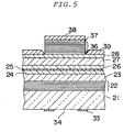
- An upper DBR mirror 36 is formed on the first p-GaAs contact layer 28 and the DBR mirror 36 is left only on the resonator region by using the lithography technique as shown in Fig. 5.
- the DBR mirror 36 is, as shown in Fig. 6A, constituted by pairing the non-doped AlAs layer 36A with a low refractive index and the non-doped GaAs layer 36B with a high refractive index and repeatedly depositing the paired layers up to 23 stages. In the GaAs layers 36B, only three In 0.20 Ga 0.80 As quantum well layers 36C with the thickness of 7 nm are formed through the GaAs layers.
- the DBR mirror 36 is grown without containing impurities.
- the total thickness of the GaAs layers 36B including the quantum well layers 36C are 69.6 nm, the thickness of one quantum well layer 36C is 7 nm, and the thickness of the AlAs layers 36A is 83.1 nm.
- the thickness of a pair of GaAs and AlAs layers is set to 152.7 nm.
- a second p-GaAs contact layer 37 with the Zn concentration of 3 x 10¹⁸atoms/cm3 is formed on the DBR mirror 36 up to the thickness of 500 nm.
- a light modulation electrode 38 comprising Ti, Pt, and Au layers is formed on the second contact layer 37 and a p-electrode 39 is formed around the upper DBR mirror 36.
- an n-electrode 33 comprising AuGe and Au layers and having a light passing hole 34 is formed at the bottom center of the GaAs substrate 21 just under the upper DBR mirror 36.
- the oscillation wavelength comes to 0.98 ⁇ m similarly to the case of the first embodiment.
- the energy band shown in Fig. 7A is obtained because the In 0.20 Ga 0.8 As quantum well layer 36C in the upper DBR mirror 36 and the In 0.20 Ga 0.8 As single quantum well active layer 25 are in the same three-dimensional system.
- the quantum well in the DBR mirror 36 has larger energy band gap between quantum levels (sub-bands) of a potential well than one in the DBR mirror 25. Thereby, the absorption loss in the DBR mirror 36 is smaller and light is effectively reflected there.
- the energy band gap of the In 0.20 Ga 0.80 As quantum well layer in the DBR mirror 36 is decreased from Eg1 to Eg2 due to the quantum-confinement Stark effect as shown in Fig. 7B and the light absorption at the wavelength ⁇ 0 extremely increases as shown in Fig. 7C.
- the refractive index also changes, the wavelength in which the reflectivity of the DBR mirror 36 is maximized gets higher than the oscillation wavelength ⁇ 0.
- the DBR mirror 36 does not include any impurity. Therefore, even if a voltage is applied to the light modulation electrode 38, current hardly flows to the resonator under the electrode 38. Thus, light is easily modulated without affecting the resonator in case of oscillation.
- the material of the quantum well layer 36C formed on the upper DBR mirror 36 is In 0.20 Ga 0.8 P and the thickness of the layer is 7 nm.
- similar modulation is realized by setting the composition ratio X of In x Ga 1-x As to, for example, 0.17 and forming the quantum well layer 36D with the thickness of 8 nm because the gap between the sub-bands of the quantum well gets larger than that of the single quantum well active layer 25 as shown in Fig. 6B.
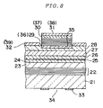
- Fig. 8 is a sectional view of the third embodiment of the present invention, in which the same symbols as those in Figs. 2A and 2B represent the same elements.
- the third embodiment is constituted by forming an n-GaAs contact layer 35 between the bottom of the upper DBR mirror 29 or 36 and the first p-GaAs contact layer 28 of the surface emitting laser of the first or second embodiment.
- Other structures of the third embodiment are the same as those of the first or second embodiment.
- the pn junction capacity at the bottom of the n-GaAs contact layer 35 gets larger than that of the lateral of the layer 35 because an electric field is applied from the light modulation electrode 31 to the p-electrode 32 (39) when applying the electric field to the DBR mirror 29 (36) by making the potential of the light modulation electrode 31 (38) positively higher than that of the p-electrode 32 (39). Therefore, the electric field applied to the DBR mirror 29 (36) becomes approximately vertically uniform to the face of the layer and modulation is easily performed.
- the above active layer 25 is constituted with a single quantum well, it is possible to constitute the layer 25 with a multiple quantum well made by forming a pair of GaAs and InGaAs layers up to a plurality of stages.
- the upper DBR mirrors 29 and 36 are not restricted to 28.5 pairs. It is possible to select the number of pairs most suitable for an optical output.
- the above embodiments use a material made of InGaAs and GaAsP. However, it is possible to use a material made of GaAs and AlGaAs or made of InGaAs and InGaAsP for the embodiments.
Landscapes
- Physics & Mathematics (AREA)
- Condensed Matter Physics & Semiconductors (AREA)
- General Physics & Mathematics (AREA)
- Electromagnetism (AREA)
- Optics & Photonics (AREA)
- Semiconductor Lasers (AREA)
Applications Claiming Priority (2)
| Application Number | Priority Date | Filing Date | Title |
|---|---|---|---|
| JP74077/93 | 1993-03-31 | ||
| JP5074077A JPH06291406A (ja) | 1993-03-31 | 1993-03-31 | 面発光半導体レーザ |
Publications (2)
| Publication Number | Publication Date |
|---|---|
| EP0618651A2 true EP0618651A2 (de) | 1994-10-05 |
| EP0618651A3 EP0618651A3 (de) | 1994-12-21 |
Family
ID=13536753
Family Applications (1)
| Application Number | Title | Priority Date | Filing Date |
|---|---|---|---|
| EP94101206A Withdrawn EP0618651A3 (de) | 1993-03-31 | 1994-01-27 | Oberflächenemittierender Laser mit Lichtmodulator. |
Country Status (3)
| Country | Link |
|---|---|
| US (1) | US5408486A (de) |
| EP (1) | EP0618651A3 (de) |
| JP (1) | JPH06291406A (de) |
Cited By (6)
| Publication number | Priority date | Publication date | Assignee | Title |
|---|---|---|---|---|
| GB2299207A (en) * | 1995-03-23 | 1996-09-25 | Samsung Electronics Co Ltd | Vertical cavity surface emitting laser |
| EP0760544A1 (de) * | 1995-08-28 | 1997-03-05 | Kabushiki Kaisha Toshiba | Monolitisch-integrierte Anordnung von lichtemittierendem Element und externem Modulator/lichtempfindlichem Element |
| GB2304423A (en) * | 1995-08-18 | 1997-03-19 | France Telecom | Tuneable wavelength laser |
| WO2004021536A1 (en) | 2002-08-28 | 2004-03-11 | Epicrystals Oy | Vertical cavity surface emitting laser comprising a modulator monolithically integrated on top |
| WO2008029283A2 (en) | 2006-06-16 | 2008-03-13 | Nikolai Ledentsov | Optoelectronic device for high-speed data transfer |
| CN102034890A (zh) * | 2009-09-25 | 2011-04-27 | 三菱电机株式会社 | 半导体光接收元件 |
Families Citing this family (19)
| Publication number | Priority date | Publication date | Assignee | Title |
|---|---|---|---|---|
| CA2121405C (en) * | 1993-04-30 | 1999-03-16 | David Andrew Barclay Miller | Tunable lasers based on absorbers in standing waves |
| US5513202A (en) * | 1994-02-25 | 1996-04-30 | Matsushita Electric Industrial Co., Ltd. | Vertical-cavity surface-emitting semiconductor laser |
| JPH08181384A (ja) * | 1994-12-21 | 1996-07-12 | Nec Corp | 面発光レーザ及びその作製方法 |
| JP2806333B2 (ja) * | 1995-11-09 | 1998-09-30 | 日本電気株式会社 | 面発光デバイスおよびその製造方法 |
| US5757837A (en) * | 1996-10-16 | 1998-05-26 | The Regents Of The University Of California | Intracavity quantum well photodetector integrated within a vertical-cavity surface-emitting laser and method of operating same |
| US5835521A (en) * | 1997-02-10 | 1998-11-10 | Motorola, Inc. | Long wavelength light emitting vertical cavity surface emitting laser and method of fabrication |
| US5892786A (en) * | 1997-03-26 | 1999-04-06 | The United States Of America As Represented By The Secretary Of The Air Force | Output control of vertical microcavity light emitting device |
| DE19727233A1 (de) * | 1997-06-26 | 1999-01-07 | Siemens Ag | Strahlungsemittierendes optoelektronisches Bauelement |
| US6810064B1 (en) * | 2000-08-22 | 2004-10-26 | The Regents Of The University Of California | Heat spreading layers for vertical cavity surface emitting lasers |
| US20020075926A1 (en) * | 2000-08-22 | 2002-06-20 | Coldren Larry A. | Current leveling layer integrated with aperture for intracavity device |
| JP2007219561A (ja) * | 2001-03-13 | 2007-08-30 | Ricoh Co Ltd | 半導体発光装置 |
| US6621836B2 (en) * | 2001-03-29 | 2003-09-16 | The United States Of America As Represented By The Secretary Of The Navy | Tunable multi-frequency vertical cavity surface emitting laser |
| US7609376B2 (en) * | 2005-01-05 | 2009-10-27 | Hewlett-Packard Development Company, L.P. | Method and apparatus for pixel display and SERS analysis |
| US7391800B2 (en) * | 2005-02-02 | 2008-06-24 | Ricoh Company, Ltd. | Vertical cavity surface-emitting semiconductor laser device, optical transmission module, optical transmission device, and optical switching method |
| JP4943052B2 (ja) * | 2006-04-27 | 2012-05-30 | 株式会社リコー | 面発光レーザ素子、面発光レーザアレイ、光走査装置、画像形成装置及び光通信システム |
| US7801197B2 (en) * | 2006-06-16 | 2010-09-21 | Epicrystals Oy | High power laser device |
| KR101598547B1 (ko) * | 2010-12-03 | 2016-03-02 | 삼성전자주식회사 | 광 이미지 변조기 및 그 제조 방법 |
| EP2525450B1 (de) | 2011-05-17 | 2017-10-04 | Danmarks Tekniske Universitet | Gitterspiegel mit Modulation der Reflektivität |
| US8948223B2 (en) | 2011-07-04 | 2015-02-03 | Danmarks Tekniske Universitet | Laser device |
Family Cites Families (6)
| Publication number | Priority date | Publication date | Assignee | Title |
|---|---|---|---|---|
| JPH0793473B2 (ja) * | 1987-10-06 | 1995-10-09 | 古河電気工業株式会社 | 光半導体素子 |
| US4949350A (en) * | 1989-07-17 | 1990-08-14 | Bell Communications Research, Inc. | Surface emitting semiconductor laser |
| JPH03290614A (ja) * | 1990-04-09 | 1991-12-20 | Nec Corp | 光変調器 |
| US5056098A (en) * | 1990-07-05 | 1991-10-08 | At&T Bell Laboratories | Vertical cavity laser with mirror having controllable reflectivity |
| US5208820A (en) * | 1991-01-08 | 1993-05-04 | Nec Corporation | Optical device with low-resistive multi-level reflecting structure |
| JPH04247676A (ja) * | 1991-02-01 | 1992-09-03 | Nippon Telegr & Teleph Corp <Ntt> | 面発光半導体モードロックレーザ |
-
1993
- 1993-03-31 JP JP5074077A patent/JPH06291406A/ja not_active Withdrawn
-
1994
- 1994-01-26 US US08/186,465 patent/US5408486A/en not_active Expired - Fee Related
- 1994-01-27 EP EP94101206A patent/EP0618651A3/de not_active Withdrawn
Cited By (10)
| Publication number | Priority date | Publication date | Assignee | Title |
|---|---|---|---|---|
| GB2299207A (en) * | 1995-03-23 | 1996-09-25 | Samsung Electronics Co Ltd | Vertical cavity surface emitting laser |
| GB2299207B (en) * | 1995-03-23 | 1999-05-12 | Samsung Electronics Co Ltd | Vertical cavity surface emitting laser |
| GB2304423A (en) * | 1995-08-18 | 1997-03-19 | France Telecom | Tuneable wavelength laser |
| GB2304423B (en) * | 1995-08-18 | 1999-05-12 | France Telecom | Tunable wavelength laser emission components |
| EP0760544A1 (de) * | 1995-08-28 | 1997-03-05 | Kabushiki Kaisha Toshiba | Monolitisch-integrierte Anordnung von lichtemittierendem Element und externem Modulator/lichtempfindlichem Element |
| US5883914A (en) * | 1995-08-28 | 1999-03-16 | Kabushiki Kaisha Toshiba | Integrated device with monolithically formed light emitting element and external modulator and integrated device with monolithically formed light emitting element and light receiving element |
| WO2004021536A1 (en) | 2002-08-28 | 2004-03-11 | Epicrystals Oy | Vertical cavity surface emitting laser comprising a modulator monolithically integrated on top |
| WO2008029283A2 (en) | 2006-06-16 | 2008-03-13 | Nikolai Ledentsov | Optoelectronic device for high-speed data transfer |
| WO2008029283A3 (en) * | 2006-06-16 | 2008-12-18 | Nikolai Ledentsov | Optoelectronic device for high-speed data transfer |
| CN102034890A (zh) * | 2009-09-25 | 2011-04-27 | 三菱电机株式会社 | 半导体光接收元件 |
Also Published As
| Publication number | Publication date |
|---|---|
| US5408486A (en) | 1995-04-18 |
| JPH06291406A (ja) | 1994-10-18 |
| EP0618651A3 (de) | 1994-12-21 |
Similar Documents
| Publication | Publication Date | Title |
|---|---|---|
| US5408486A (en) | Surface emitting laser provided with light modulator | |
| US5491710A (en) | Strain-compensated multiple quantum well laser structures | |
| JP2692913B2 (ja) | グレーティング結合型表面発光レーザ素子およびその変調方法 | |
| US8419956B2 (en) | Surface emitting photonic device | |
| US5539763A (en) | Semiconductor lasers and methods for fabricating semiconductor lasers | |
| US5042049A (en) | Semiconductor optical device | |
| US5023878A (en) | Apparatus comprising a quantum well device and method of operating the apparatus | |
| JP2003069144A (ja) | 分布帰還型半導体レーザ素子 | |
| US5280493A (en) | Quantum wire laser | |
| US10243330B2 (en) | Optoelectronic device with resonant suppression of high order optical modes and method of making same | |
| JP2001320125A (ja) | 半導体レーザ素子 | |
| JP2871288B2 (ja) | 面型光半導体素子およびその製造方法 | |
| EP4246741A1 (de) | Kaskadenlaser mit vertikaler emission | |
| EP0386634B1 (de) | Halbleiterlaser-Anordnung | |
| JP3971600B2 (ja) | レーザダイオード | |
| JPH0563301A (ja) | 半導体光素子および光通信システム | |
| US5182758A (en) | Periodic gain-type semiconductor laser device | |
| JPH05327111A (ja) | 半導体レーザ装置及びその製造方法 | |
| US5309472A (en) | Semiconductor device and a method for producing the same | |
| JP3911002B2 (ja) | 半導体レーザ素子 | |
| JP3949704B2 (ja) | 半導体レーザ素子 | |
| JP3943233B2 (ja) | 光半導体装置 | |
| JP2001257421A (ja) | 半導体レーザ素子および製造方法 | |
| JPH0537068A (ja) | 半導体レーザ | |
| JPH1117271A (ja) | 半導体レーザ |
Legal Events
| Date | Code | Title | Description |
|---|---|---|---|
| PUAI | Public reference made under article 153(3) epc to a published international application that has entered the european phase |
Free format text: ORIGINAL CODE: 0009012 |
|
| AK | Designated contracting states |
Kind code of ref document: A2 Designated state(s): DE FR GB |
|
| PUAL | Search report despatched |
Free format text: ORIGINAL CODE: 0009013 |
|
| AK | Designated contracting states |
Kind code of ref document: A3 Designated state(s): DE FR GB |
|
| 17P | Request for examination filed |
Effective date: 19950616 |
|
| 17Q | First examination report despatched |
Effective date: 19970129 |
|
| STAA | Information on the status of an ep patent application or granted ep patent |
Free format text: STATUS: THE APPLICATION IS DEEMED TO BE WITHDRAWN |
|
| 18D | Application deemed to be withdrawn |
Effective date: 19970610 |