EP0619615A2 - Arsen-Passivierung für die epitaktische Ablagerung von ternären Chalcogenid-Halbleiterschichten auf Silizium Substraten - Google Patents
Arsen-Passivierung für die epitaktische Ablagerung von ternären Chalcogenid-Halbleiterschichten auf Silizium Substraten Download PDFInfo
- Publication number
- EP0619615A2 EP0619615A2 EP94105102A EP94105102A EP0619615A2 EP 0619615 A2 EP0619615 A2 EP 0619615A2 EP 94105102 A EP94105102 A EP 94105102A EP 94105102 A EP94105102 A EP 94105102A EP 0619615 A2 EP0619615 A2 EP 0619615A2
- Authority
- EP
- European Patent Office
- Prior art keywords
- group
- monolayer
- ternary
- multilayer stack
- arsenic
- Prior art date
- Legal status (The legal status is an assumption and is not a legal conclusion. Google has not performed a legal analysis and makes no representation as to the accuracy of the status listed.)
- Withdrawn
Links
Images
Classifications
-
- C—CHEMISTRY; METALLURGY
- C30—CRYSTAL GROWTH
- C30B—SINGLE-CRYSTAL GROWTH; UNIDIRECTIONAL SOLIDIFICATION OF EUTECTIC MATERIAL OR UNIDIRECTIONAL DEMIXING OF EUTECTOID MATERIAL; REFINING BY ZONE-MELTING OF MATERIAL; PRODUCTION OF A HOMOGENEOUS POLYCRYSTALLINE MATERIAL WITH DEFINED STRUCTURE; SINGLE CRYSTALS OR HOMOGENEOUS POLYCRYSTALLINE MATERIAL WITH DEFINED STRUCTURE; AFTER-TREATMENT OF SINGLE CRYSTALS OR A HOMOGENEOUS POLYCRYSTALLINE MATERIAL WITH DEFINED STRUCTURE; APPARATUS THEREFOR
- C30B23/00—Single-crystal growth by condensing evaporated or sublimed materials
- C30B23/02—Epitaxial-layer growth
-
- C—CHEMISTRY; METALLURGY
- C30—CRYSTAL GROWTH
- C30B—SINGLE-CRYSTAL GROWTH; UNIDIRECTIONAL SOLIDIFICATION OF EUTECTIC MATERIAL OR UNIDIRECTIONAL DEMIXING OF EUTECTOID MATERIAL; REFINING BY ZONE-MELTING OF MATERIAL; PRODUCTION OF A HOMOGENEOUS POLYCRYSTALLINE MATERIAL WITH DEFINED STRUCTURE; SINGLE CRYSTALS OR HOMOGENEOUS POLYCRYSTALLINE MATERIAL WITH DEFINED STRUCTURE; AFTER-TREATMENT OF SINGLE CRYSTALS OR A HOMOGENEOUS POLYCRYSTALLINE MATERIAL WITH DEFINED STRUCTURE; APPARATUS THEREFOR
- C30B25/00—Single-crystal growth by chemical reaction of reactive gases, e.g. chemical vapour-deposition growth
- C30B25/02—Epitaxial-layer growth
-
- C—CHEMISTRY; METALLURGY
- C30—CRYSTAL GROWTH
- C30B—SINGLE-CRYSTAL GROWTH; UNIDIRECTIONAL SOLIDIFICATION OF EUTECTIC MATERIAL OR UNIDIRECTIONAL DEMIXING OF EUTECTOID MATERIAL; REFINING BY ZONE-MELTING OF MATERIAL; PRODUCTION OF A HOMOGENEOUS POLYCRYSTALLINE MATERIAL WITH DEFINED STRUCTURE; SINGLE CRYSTALS OR HOMOGENEOUS POLYCRYSTALLINE MATERIAL WITH DEFINED STRUCTURE; AFTER-TREATMENT OF SINGLE CRYSTALS OR A HOMOGENEOUS POLYCRYSTALLINE MATERIAL WITH DEFINED STRUCTURE; APPARATUS THEREFOR
- C30B29/00—Single crystals or homogeneous polycrystalline material with defined structure characterised by the material or by their shape
- C30B29/10—Inorganic compounds or compositions
- C30B29/46—Sulfur-, selenium- or tellurium-containing compounds
- C30B29/48—AIIBVI compounds wherein A is Zn, Cd or Hg, and B is S, Se or Te
-
- H—ELECTRICITY
- H10—SEMICONDUCTOR DEVICES; ELECTRIC SOLID-STATE DEVICES NOT OTHERWISE PROVIDED FOR
- H10P—GENERIC PROCESSES OR APPARATUS FOR THE MANUFACTURE OR TREATMENT OF DEVICES COVERED BY CLASS H10
- H10P14/00—Formation of materials, e.g. in the shape of layers or pillars
- H10P14/20—Formation of materials, e.g. in the shape of layers or pillars of semiconductor materials
- H10P14/29—Formation of materials, e.g. in the shape of layers or pillars of semiconductor materials characterised by the substrates
- H10P14/2901—Materials
- H10P14/2902—Materials being Group IVA materials
- H10P14/2905—Silicon, silicon germanium or germanium
-
- H—ELECTRICITY
- H10—SEMICONDUCTOR DEVICES; ELECTRIC SOLID-STATE DEVICES NOT OTHERWISE PROVIDED FOR
- H10P—GENERIC PROCESSES OR APPARATUS FOR THE MANUFACTURE OR TREATMENT OF DEVICES COVERED BY CLASS H10
- H10P14/00—Formation of materials, e.g. in the shape of layers or pillars
- H10P14/20—Formation of materials, e.g. in the shape of layers or pillars of semiconductor materials
- H10P14/29—Formation of materials, e.g. in the shape of layers or pillars of semiconductor materials characterised by the substrates
- H10P14/2926—Crystal orientations
-
- H—ELECTRICITY
- H10—SEMICONDUCTOR DEVICES; ELECTRIC SOLID-STATE DEVICES NOT OTHERWISE PROVIDED FOR
- H10P—GENERIC PROCESSES OR APPARATUS FOR THE MANUFACTURE OR TREATMENT OF DEVICES COVERED BY CLASS H10
- H10P14/00—Formation of materials, e.g. in the shape of layers or pillars
- H10P14/20—Formation of materials, e.g. in the shape of layers or pillars of semiconductor materials
- H10P14/32—Formation of materials, e.g. in the shape of layers or pillars of semiconductor materials characterised by intermediate layers between substrates and deposited layers
- H10P14/3202—Materials thereof
-
- H—ELECTRICITY
- H10—SEMICONDUCTOR DEVICES; ELECTRIC SOLID-STATE DEVICES NOT OTHERWISE PROVIDED FOR
- H10P—GENERIC PROCESSES OR APPARATUS FOR THE MANUFACTURE OR TREATMENT OF DEVICES COVERED BY CLASS H10
- H10P14/00—Formation of materials, e.g. in the shape of layers or pillars
- H10P14/20—Formation of materials, e.g. in the shape of layers or pillars of semiconductor materials
- H10P14/32—Formation of materials, e.g. in the shape of layers or pillars of semiconductor materials characterised by intermediate layers between substrates and deposited layers
- H10P14/3242—Structure
- H10P14/3244—Layer structure
- H10P14/3246—Monolayers
-
- H—ELECTRICITY
- H10—SEMICONDUCTOR DEVICES; ELECTRIC SOLID-STATE DEVICES NOT OTHERWISE PROVIDED FOR
- H10P—GENERIC PROCESSES OR APPARATUS FOR THE MANUFACTURE OR TREATMENT OF DEVICES COVERED BY CLASS H10
- H10P14/00—Formation of materials, e.g. in the shape of layers or pillars
- H10P14/20—Formation of materials, e.g. in the shape of layers or pillars of semiconductor materials
- H10P14/34—Deposited materials, e.g. layers
- H10P14/3402—Deposited materials, e.g. layers characterised by the chemical composition
- H10P14/3424—Deposited materials, e.g. layers characterised by the chemical composition being Group IIB-VIA materials
- H10P14/3432—Tellurides
-
- H—ELECTRICITY
- H10—SEMICONDUCTOR DEVICES; ELECTRIC SOLID-STATE DEVICES NOT OTHERWISE PROVIDED FOR
- H10P—GENERIC PROCESSES OR APPARATUS FOR THE MANUFACTURE OR TREATMENT OF DEVICES COVERED BY CLASS H10
- H10P14/00—Formation of materials, e.g. in the shape of layers or pillars
- H10P14/20—Formation of materials, e.g. in the shape of layers or pillars of semiconductor materials
- H10P14/34—Deposited materials, e.g. layers
- H10P14/3466—Crystal orientation
-
- Y—GENERAL TAGGING OF NEW TECHNOLOGICAL DEVELOPMENTS; GENERAL TAGGING OF CROSS-SECTIONAL TECHNOLOGIES SPANNING OVER SEVERAL SECTIONS OF THE IPC; TECHNICAL SUBJECTS COVERED BY FORMER USPC CROSS-REFERENCE ART COLLECTIONS [XRACs] AND DIGESTS
- Y10—TECHNICAL SUBJECTS COVERED BY FORMER USPC
- Y10S—TECHNICAL SUBJECTS COVERED BY FORMER USPC CROSS-REFERENCE ART COLLECTIONS [XRACs] AND DIGESTS
- Y10S148/00—Metal treatment
- Y10S148/064—Gp II-VI compounds
-
- Y—GENERAL TAGGING OF NEW TECHNOLOGICAL DEVELOPMENTS; GENERAL TAGGING OF CROSS-SECTIONAL TECHNOLOGIES SPANNING OVER SEVERAL SECTIONS OF THE IPC; TECHNICAL SUBJECTS COVERED BY FORMER USPC CROSS-REFERENCE ART COLLECTIONS [XRACs] AND DIGESTS
- Y10—TECHNICAL SUBJECTS COVERED BY FORMER USPC
- Y10S—TECHNICAL SUBJECTS COVERED BY FORMER USPC CROSS-REFERENCE ART COLLECTIONS [XRACs] AND DIGESTS
- Y10S438/00—Semiconductor device manufacturing: process
- Y10S438/93—Ternary or quaternary semiconductor comprised of elements from three different groups, e.g. I-III-V
-
- Y—GENERAL TAGGING OF NEW TECHNOLOGICAL DEVELOPMENTS; GENERAL TAGGING OF CROSS-SECTIONAL TECHNOLOGIES SPANNING OVER SEVERAL SECTIONS OF THE IPC; TECHNICAL SUBJECTS COVERED BY FORMER USPC CROSS-REFERENCE ART COLLECTIONS [XRACs] AND DIGESTS
- Y10—TECHNICAL SUBJECTS COVERED BY FORMER USPC
- Y10S—TECHNICAL SUBJECTS COVERED BY FORMER USPC CROSS-REFERENCE ART COLLECTIONS [XRACs] AND DIGESTS
- Y10S438/00—Semiconductor device manufacturing: process
- Y10S438/933—Germanium or silicon or Ge-Si on III-V
Definitions
- the present invention relates to the deposition of II-VI semiconductor films, and, more particularly, to the deposition of ternary chalcogenide semiconductor films, such as HgCdTe and HgZnTe, onto silicon substrates.
- Ternary II-VI semiconductor films find use in many infra-red applications, such as in IR focal plane arrays (FPAs).
- FPAs focal plane arrays
- ternary II-VI semiconductor compounds include HgCdTe and HgZnTe, which are also known as chalcogenides.
- ternary II-VI semiconductors were formed on ternary II-VI substrates, such as CdZnTe, which were then bonded to silicon substrates by indium bump technology.
- CdZnTe ternary II-VI substrates
- the thermal cycling to 77K which is the temperature used for detection, has tended to create reliability problems. It is desired to use silicon-based substrates rather than bulk CdZnTe substrates for large area focal plane arrays, since the read-out circuit chips are also silicon, and thus expansion and contraction with thermal cycling would be at the same rate.
- Group II fluoride buffer layers on silicon have been used, with the II-VI film formed on the buffer layer; see, e.g., A.N. Tiwari, et al., "Heteroepitaxy of CdTe(100) on Si(100) Using BaF2-CaF2(100) Buffer Layers", Journal of Crystal Growth , Vol. 111, pp. 730-735 (1991).
- this approach is presently substantially inferior in crystalline quality to II-VI films deposited either on GaAs/Si or silicon.
- silicon substrates with a buffer layer of GaAs are generally obtained from an outside vendor and cost approximately $2,000 (1993 dollars) for a 4-inch diameter wafer versus a cost of $20 for a comparable uncoated silicon wafer.
- Purchase of GaAs-on-Si substrates also requires reliance on the quality control protocols of two separate manufacturers - the silicon substrate supplier and GaAs epitaxial foundry.
- ternary II-VI semiconductor films are formed on a silicon substrate by depositing a monolayer of arsenic on a cleaned surface of the substrate. The ternary II-VI semiconductor film is then formed over the arsenic monolayer, either directly or on top of an intermediate II-VI semiconductor buffer layer.
- the novelty of the present invention comprises the use of an arsenic passivating layer to facilitate the epitaxial deposition of technologically important II-VI semiconductors such as ZnTe, CdTe, and HgCdTe on silicon substrates of arbitrary crystallographic orientation.
- II-VI semiconductors such as ZnTe, CdTe, and HgCdTe
- Prior attempts to deposit such films have relied on GaAs-on-Si composite substrates, which are expensive, difficult to prepare for epitaxy, and present potential III-V doping contaminants to HgCdTe epitaxy systems.
- Preparation of Si substrates with a simple monolayer of arsenic atoms enables subsequent high quality molecular beam epitaxy or metal-organic chemical vapor deposition growth of highly lattice-mismatched II-VI epitaxial films such as ZnTe, CdTe, HgZnTe, and HgCdTe without the complication of additional thick interlayers.
- the present invention enables the deposition of good quality II-VI epitaxial films on silicon substrates without the complications of previously demonstrated methods employing less desirable intervening layers between the silicon substrate and the II-VI epitaxial film.
- Elimination of the GaAs layer is also an advantage because of the difficulty of properly removing the GaAs native oxide and preparing a stoichiometric GaAs semiconductor surface prior to molecular beam epitaxy (MBE) deposition of the II-VI film.
- MBE molecular beam epitaxy
- CdTe films deposited on GaAs-on-Si exhibit crystalline perfection comparable to that of CdTe films deposited on As-passivated Si, but quite often the morphological quality, either from MOCVD (S.M. Johnson, et al., "Structural and Electrical Properties of Heteroepitaxial HgCdTe/CdZnTe/GaAs/Si", Materials Research Society Symposium Proceedings , Vol. 161, pp. 351-356 (1990) or MBE, is much worse than that which is routinely achieved with growth on As-passivated silicon.
- ternary II-VI films may be grown either on ZnSe or directly on the arsenic layer.
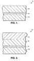
- FIG. 1 shows a schematic cross-section 10 of a multi-layer stack of II-VI epitaxial films designed to function as a conventional infrared photovoltaic detector.
- the crucial first step in the process is the deposition on a silicon substrate 12 of a single monolayer 14 of arsenic, such as by MBE or MOCVD or perhaps through appropriate ex situ wet chemical treatment, prior to the initiation of II-VI epitaxy.
- the arsenic deposition procedure must be designed to deposit only a single monolayer of arsenic on an atomically clean Si surface; deposition of quantities of arsenic in excess of this is unacceptable and will disrupt the subsequent epitaxial processes.
- the epitaxial growth sequence must furthermore be designed to allow a single, uncontaminated monolayer of arsenic to remain on the silicon surface during the time period between the completion of the actual arsenic deposition and the commencement of II-VI layer deposition.
- the arsenic monolayer 14 may be deposited by any of the conventional deposition processes known in the art, such as MBE, MOCVD, metal organic MBE (MOMBE), and gas source MBE (GSMBE), using elemental As or other As-containing precursors such as arsine or t -butyl arsine.
- MBE metal organic MBE
- GSMBE gas source MBE
- elemental As or other As-containing precursors such as arsine or t -butyl arsine.
- a wet chemical process executed immediately prior to loading the Si substrates into a II-VI epitaxial reactor, could be utilized to terminate the Si surface with As through chemical reactions in a liquid environment.
- the monolayer 14 may alternatively comprise other elements from Group V of the Periodic Table, specifically, phosphorus or antimony.
- II-VI epilayer After the monolayer passivation of the silicon surface, the growth of II-VI epilayer, such as by MBE or MOCVD, can be initiated with one or more II-VI epilayers 16 , as shown in FIG. 1.
- the sequence of II-VI epilayers 16 is typically grown to a total thickness ranging from about 10 to 15 ⁇ m for conventional IR detector structures. Devices are then formed in the top surface of the epilayer 16 .
- the II-VI epilayer 16 comprises any of the binary, ternary and quaternary II-VI semiconductor compounds, and preferably comprises binaries such as ZnTe, CdTe, CdSe, CdS, and ZnS, ternaries such as HgCdTe, HgZnTe, HgCdSe, HgZnSe, HgCdS, and HgZnS, and quaternaries such as ZnCdSeTe, ZnCdSSe, ZnCdSTe, HgCdZnTe, HgCdSeTe, and HgZnSeTe.
- binaries such as ZnTe, CdTe, CdSe, CdS, and ZnS
- ternaries such as HgCdTe, HgZnTe, HgCdSe, HgZnSe, HgCdS, and HgZnSeTe.
- any sequence of II-VI buffer layers 18 may be deposited on the passivating monolayer 14 , followed by growth of the II-VI epilayer 16 thereon, as shown in FIG. 2.
- the completed multilayer stack is denoted 10' in FIG. 2.
- the II-VI buffer layer 18 is grown to a thickness ranging from about 8 to 10 ⁇ m.
- the final device structure comprises one or more II-VI epilayer layers 16 , which can be grown by either LPE, MBE, or MOCVD.
- the II-VI buffer layer 18 may comprise any of sulfur-, selenium-, or tellurium-containing binary II-VI compounds such as BeS, MgS, ZnS, CdS, HgS, MnS, BeTe, MgTe, ZnTe, CdTe, HgTe, CdSe, and ZnSe, and any of the ternary II-VI compounds, such as ZnSSe, ZnSTe, ZnSeTe, CdSSe, CdSTe, CdZnSe, CdZnTe, HgCdTe, HgZnTe, HgCdSe, and HgZnSe. Further, any combination of the foregoing binary and ternary compounds may be used in a multilayer stack to form the buffer layer 18 .
- binary II-VI compounds such as BeS, MgS, ZnS, CdS, HgS, MnS, BeTe, MgTe, ZnTe, Cd
- preferred binaries include ZnTe, CdTe, CdSe, and CdS
- preferred ternaries include CdZnTe, CdSeTe, CdZnSe, and ZnTeSe.
- the buffer layer 18 comprises a II-VI material having as low a microhardness as possible (relative to the final ternary II-VI device structure), since this would ensure that dislocations generated either during growth due to the lattice mismatch or those introduced during post-growth thermal annealing (LPE growth of HgCdTe typically takes the wafer to about 500°C) would have the highest probability of confinement in the buffer layer.
- the As passivation 14 is crucial to facilitating the high quality deposition of the II-VI epilayer 16 or, if employed, the II-VI buffer layer 18 , whose chemical identity could be quite broad.
- the technique of As passivation may furthermore be extended to Si substrate orientations other than ⁇ 100 ⁇ , such as ⁇ 111 ⁇ and ⁇ 211 ⁇ , which are also of technological importance.
- arsenic serves two functions. First, it acts as a barrier to prevent spurious chemical reactions between Group VI species, such as Te, and the Si substrate that could potentially disrupt the epitaxial process. Second, a plane of Group VI atoms has the correct chemical valence for full chemical coordination between a plane of Group IV atoms and a plane of Group II atoms from a II-VI compound, which serves to ensure the chemical stability of the interface.
- the present invention has been reduced to practice using a composite buffer layer consisting of CdZnTe and ZnTe grown on As-passivated Si(100).
- a buffer layer 18 consisting of 1 ⁇ m of ZnTe followed by 9 ⁇ m of CdZnTe was deposited by MBE on a silicon substrate 12 passivated with an arsenic monolayer 14 .
- the thin ZnTe layer acts to ensure (100)-oriented growth of the CdZnTe layer.
- a HgCdTe epilayer 16 was deposited by LPE on this CdZnTe/ZnTe/As/Si structure.
- a rocking curve of the HgCdTe was obtained having a value of full-width at half-maximum (FWHM) of less than 60 arc seconds, which compares favorably with 70 to 110 arc seconds generally obtained for HgCdTe deposited on CdZnTe/ZnTe/GaAs/Si substrates.
- FWHM full-width at half-maximum
- the surface morphology of such buffer layers on As-passivated silicon was superior to that which is generally obtained on GaAs-on-Si.
- Preliminary etch pit density measurements indicated comparable threading dislocation densities of 2 to 3x105 cm ⁇ 2 in CdZnTe buffer layers grown on both As-passivated Si and GaAs-on-Si.
- the present invention is expected to have an economic impact on efforts to produce large area infrared focal-plane arrays (FPAs) on alternative substrates. It is desirable to use Si-based substrates rather than bulk CdZnTe substrates for large area FPA fabrication because of wafer material and processing cost savings and to improve the thermal cycle reliability of indium bump bonds used to hybridize FPAs to silicon readout chips.
- FPAs focal-plane arrays
- Si-based substrates cost can be reduced approximately one hundred-fold, from $2000/GaAs-on-Si wafer to $20/Si wafer for 4-inch substrates, and the cost of substrate quality screening can also be expected to drop substantially.
Landscapes
- Chemical & Material Sciences (AREA)
- Engineering & Computer Science (AREA)
- Crystallography & Structural Chemistry (AREA)
- Materials Engineering (AREA)
- Metallurgy (AREA)
- Organic Chemistry (AREA)
- Chemical Kinetics & Catalysis (AREA)
- General Chemical & Material Sciences (AREA)
- Inorganic Chemistry (AREA)
- Physical Deposition Of Substances That Are Components Of Semiconductor Devices (AREA)
- Recrystallisation Techniques (AREA)
Applications Claiming Priority (2)
| Application Number | Priority Date | Filing Date | Title |
|---|---|---|---|
| US08/043,644 US5306386A (en) | 1993-04-06 | 1993-04-06 | Arsenic passivation for epitaxial deposition of ternary chalcogenide semiconductor films onto silicon substrates |
| US43644 | 2002-01-10 |
Publications (2)
| Publication Number | Publication Date |
|---|---|
| EP0619615A2 true EP0619615A2 (de) | 1994-10-12 |
| EP0619615A3 EP0619615A3 (de) | 1995-03-15 |
Family
ID=21928166
Family Applications (1)
| Application Number | Title | Priority Date | Filing Date |
|---|---|---|---|
| EP94105102A Withdrawn EP0619615A3 (de) | 1993-04-06 | 1994-03-31 | Arsen-Passivierung für die epitaktische Ablagerung von ternären Chalcogenid-Halbleiterschichten auf Silizium Substraten. |
Country Status (4)
| Country | Link |
|---|---|
| US (2) | US5306386A (de) |
| EP (1) | EP0619615A3 (de) |
| JP (1) | JPH076951A (de) |
| IL (1) | IL109194A (de) |
Cited By (3)
| Publication number | Priority date | Publication date | Assignee | Title |
|---|---|---|---|---|
| WO1995031824A1 (en) * | 1994-05-16 | 1995-11-23 | Santa Barbara Research Center | Multilayer buffer structure including ii-vi compounds on a silicon substrate |
| WO2005098097A1 (en) * | 2004-04-06 | 2005-10-20 | Qinetiq Limited | Manufacture of cadmium mercury telluride |
| US7892879B2 (en) | 2004-08-02 | 2011-02-22 | Qinetiq Limited | Manufacture of cadmium mercury telluride on patterned silicon |
Families Citing this family (33)
| Publication number | Priority date | Publication date | Assignee | Title |
|---|---|---|---|---|
| US5477809A (en) * | 1993-06-23 | 1995-12-26 | Nec Corporation | Method of growth of CdTe on silicon by molecular beam epitaxy |
| JPH08107068A (ja) * | 1994-10-03 | 1996-04-23 | Nec Corp | MBE法によるSi基板上CdTe成長方法 |
| US6419742B1 (en) * | 1994-11-15 | 2002-07-16 | Texas Instruments Incorporated | method of forming lattice matched layer over a surface of a silicon substrate |
| US5742089A (en) * | 1995-06-07 | 1998-04-21 | Hughes Electronics | Growth of low dislocation density HGCDTE detector structures |
| US6010937A (en) * | 1995-09-05 | 2000-01-04 | Spire Corporation | Reduction of dislocations in a heteroepitaxial semiconductor structure |
| US5879962A (en) * | 1995-12-13 | 1999-03-09 | Minnesota Mining And Manufacturing Company | III-V/II-VI Semiconductor interface fabrication method |
| US5872016A (en) * | 1996-06-18 | 1999-02-16 | Lucent Technologies Inc. | Process of making an optoelectronic devices utilizing multiple quantum well pin structures |
| US6090637A (en) * | 1997-02-13 | 2000-07-18 | 3M Innovative Properties Company | Fabrication of II-VI semiconductor device with BeTe buffer layer |
| US5998235A (en) * | 1997-06-26 | 1999-12-07 | Lockheed Martin Corporation | Method of fabrication for mercury-based quaternary alloys of infrared sensitive materials |
| DE19729186A1 (de) * | 1997-07-08 | 1999-01-14 | Siemens Ag | Verfahren zum Herstellen eines II-VI-Halbleiter-Bauelements |
| US6064078A (en) * | 1998-05-22 | 2000-05-16 | Xerox Corporation | Formation of group III-V nitride films on sapphire substrates with reduced dislocation densities |
| US6833556B2 (en) * | 2002-08-12 | 2004-12-21 | Acorn Technologies, Inc. | Insulated gate field effect transistor having passivated schottky barriers to the channel |
| US7176483B2 (en) * | 2002-08-12 | 2007-02-13 | Acorn Technologies, Inc. | Method for depinning the Fermi level of a semiconductor at an electrical junction and devices incorporating such junctions |
| US7084423B2 (en) | 2002-08-12 | 2006-08-01 | Acorn Technologies, Inc. | Method for depinning the Fermi level of a semiconductor at an electrical junction and devices incorporating such junctions |
| US7902029B2 (en) * | 2002-08-12 | 2011-03-08 | Acorn Technologies, Inc. | Process for fabricating a self-aligned deposited source/drain insulated gate field-effect transistor |
| JP4131498B2 (ja) * | 2003-11-27 | 2008-08-13 | 財団法人名古屋産業科学研究所 | 半導体放射線検出器 |
| US7518207B1 (en) | 2004-03-19 | 2009-04-14 | The United States Of America As Represented By The Secretary Of The Navy | Molecular beam epitaxy growth of ternary and quaternary metal chalcogenide films |
| GB2433648A (en) * | 2005-12-21 | 2007-06-27 | Durham Scient Crystals Ltd | Radiation detector formed by deposition of bulk semiconductor crystal layers |
| JP5662001B2 (ja) * | 2005-12-21 | 2015-01-28 | クロメック リミテッド | 半導体デバイス及びその製造方法 |
| US7923688B2 (en) * | 2007-10-31 | 2011-04-12 | Raytheon Company | Multiple-band detector using frequency selective slots |
| US7972938B2 (en) * | 2008-06-05 | 2011-07-05 | Ues, Inc. | Methods of splitting CdZnTe layers from CdZnTe substrates for the growth of HgCdTe |
| US7923689B2 (en) * | 2009-04-30 | 2011-04-12 | Raytheon Company | Multi-band sub-wavelength IR detector having frequency selective slots and method of making the same |
| US8053734B2 (en) * | 2009-04-30 | 2011-11-08 | Raytehon Company | Nano-antenna for wideband coherent conformal IR detector arrays |
| US9837563B2 (en) * | 2009-12-17 | 2017-12-05 | Epir Technologies, Inc. | MBE growth technique for group II-VI inverted multijunction solar cells |
| CN103348488B (zh) * | 2010-09-22 | 2016-08-03 | 第一太阳能有限公司 | 具有金属硫氧化物窗口层的光伏装置 |
| US8993418B2 (en) | 2010-11-19 | 2015-03-31 | Commissariat A L'energie Atomique Et Aux Energies Alternatives | Shallow heavily doped semiconductor layer by cyclic selective epitaxial deposition process |
| US8772873B2 (en) | 2011-01-24 | 2014-07-08 | Tsinghua University | Ge-on-insulator structure and method for forming the same |
| CN102157432A (zh) * | 2011-01-24 | 2011-08-17 | 清华大学 | GeOI结构及其形成方法 |
| US9553116B2 (en) * | 2014-06-05 | 2017-01-24 | Teledyne Scientific & Imaging, Llc | Imaging detector having an integrated wide bandgap layer and method of manufacturing thereof |
| US9620611B1 (en) | 2016-06-17 | 2017-04-11 | Acorn Technology, Inc. | MIS contact structure with metal oxide conductor |
| DE112017005855T5 (de) | 2016-11-18 | 2019-08-01 | Acorn Technologies, Inc. | Nanodrahttransistor mit Source und Drain induziert durch elektrische Kontakte mit negativer Schottky-Barrierenhöhe |
| US20190229226A1 (en) * | 2018-01-22 | 2019-07-25 | Uriel Solar, Inc. | Wide Band-Gap II-VI Heterojunction Solar Cell for Use In Tandem Structure |
| US11121302B2 (en) | 2018-10-11 | 2021-09-14 | SeeQC, Inc. | System and method for superconducting multi-chip module |
Family Cites Families (10)
| Publication number | Priority date | Publication date | Assignee | Title |
|---|---|---|---|---|
| BE758613A (fr) * | 1969-11-06 | 1971-05-06 | Consortium Elektrochem Ind | Procede et dispositif de fabrication de couches semi-conductrices epitactiques |
| US4935385A (en) * | 1988-07-22 | 1990-06-19 | Xerox Corporation | Method of forming intermediate buffer films with low plastic deformation threshold using lattice mismatched heteroepitaxy |
| JPH0239441A (ja) * | 1988-07-28 | 1990-02-08 | Fujitsu Ltd | 化合物半導体結晶の製造方法 |
| JPH0244736A (ja) * | 1988-08-05 | 1990-02-14 | Fujitsu Ltd | 化合物半導体結晶の製造方法 |
| US4931132A (en) * | 1988-10-07 | 1990-06-05 | Bell Communications Research, Inc. | Optical control of deposition of crystal monolayers |
| US4910154A (en) * | 1988-12-23 | 1990-03-20 | Ford Aerospace Corporation | Manufacture of monolithic infrared focal plane arrays |
| US5028561A (en) * | 1989-06-15 | 1991-07-02 | Hughes Aircraft Company | Method of growing p-type group II-VI material |
| US5021360A (en) * | 1989-09-25 | 1991-06-04 | Gte Laboratories Incorporated | Method of farbicating highly lattice mismatched quantum well structures |
| US5013685A (en) * | 1989-11-02 | 1991-05-07 | At&T Bell Laboratories | Method of making a non-alloyed ohmic contact to III-V semiconductors-on-silicon |
| JP2557546B2 (ja) * | 1990-03-30 | 1996-11-27 | 三菱電機株式会社 | 半導体装置の製造方法 |
-
1993
- 1993-04-06 US US08/043,644 patent/US5306386A/en not_active Expired - Lifetime
- 1993-09-08 US US08/118,084 patent/US5399206A/en not_active Expired - Lifetime
-
1994
- 1994-03-31 EP EP94105102A patent/EP0619615A3/de not_active Withdrawn
- 1994-03-31 IL IL10919494A patent/IL109194A/en not_active IP Right Cessation
- 1994-04-05 JP JP6067402A patent/JPH076951A/ja active Pending
Cited By (4)
| Publication number | Priority date | Publication date | Assignee | Title |
|---|---|---|---|---|
| WO1995031824A1 (en) * | 1994-05-16 | 1995-11-23 | Santa Barbara Research Center | Multilayer buffer structure including ii-vi compounds on a silicon substrate |
| WO2005098097A1 (en) * | 2004-04-06 | 2005-10-20 | Qinetiq Limited | Manufacture of cadmium mercury telluride |
| US8021914B2 (en) | 2004-04-06 | 2011-09-20 | Qinetiq Limited | Manufacture of cadmium mercury telluride |
| US7892879B2 (en) | 2004-08-02 | 2011-02-22 | Qinetiq Limited | Manufacture of cadmium mercury telluride on patterned silicon |
Also Published As
| Publication number | Publication date |
|---|---|
| US5399206A (en) | 1995-03-21 |
| IL109194A0 (en) | 1994-06-24 |
| EP0619615A3 (de) | 1995-03-15 |
| IL109194A (en) | 1996-10-16 |
| US5306386A (en) | 1994-04-26 |
| JPH076951A (ja) | 1995-01-10 |
Similar Documents
| Publication | Publication Date | Title |
|---|---|---|
| US5306386A (en) | Arsenic passivation for epitaxial deposition of ternary chalcogenide semiconductor films onto silicon substrates | |
| US5019529A (en) | Heteroepitaxial growth method | |
| US5394826A (en) | Method of (111) group II-VI epitaxial layer grown on (111) silicon substrate | |
| US4960728A (en) | Homogenization anneal of II-VI compounds | |
| US6667252B2 (en) | Method of manufacturing compound semiconductor substrate | |
| US5107317A (en) | Semiconductor device with first and second buffer layers | |
| JP2570646B2 (ja) | Siベ−ス半導体結晶基板及びその製造方法 | |
| US5449927A (en) | Multilayer buffer structure including II-VI compounds on a silicon substrate | |
| US5016065A (en) | Compound semiconductor substrate with InGaP layer | |
| JP3007971B1 (ja) | 単結晶薄膜の形成方法 | |
| US5492860A (en) | Method for growing compound semiconductor layers | |
| Bachmann et al. | Heteroepitaxy of lattice‐matched compound semiconductors on silicon | |
| US6419742B1 (en) | method of forming lattice matched layer over a surface of a silicon substrate | |
| US5204283A (en) | Method of growth II-VI semiconducting compounds | |
| JP3333346B2 (ja) | 半導体装置 | |
| US7687798B2 (en) | Epitaxy with compliant layers of group-V species | |
| Grundmann et al. | Antiphase-domain-free InP on Si (001): Optimization of MOCVD process | |
| US5183778A (en) | Method of producing a semiconductor device | |
| de Lyon et al. | Direct MBE growth of HgCdTe (112) IR detector structures on Si (112) substrates | |
| Bringans et al. | initial Stages of Growth of ZnSe on Si | |
| WO2024132142A1 (en) | Method of fabricating a device, device, and deposition apparatus | |
| JPH0697401A (ja) | 半導体装置およびその製造方法 | |
| JP3052399B2 (ja) | 化合物半導体膜の製造方法 | |
| JP2503255B2 (ja) | 化合物半導体基板の製造方法 | |
| Nishinaga | Microchannel Epitaxy-Physics of Lateral and Vertical Growth and its Applications |
Legal Events
| Date | Code | Title | Description |
|---|---|---|---|
| PUAI | Public reference made under article 153(3) epc to a published international application that has entered the european phase |
Free format text: ORIGINAL CODE: 0009012 |
|
| AK | Designated contracting states |
Kind code of ref document: A2 Designated state(s): DE FR GB IT NL |
|
| PUAL | Search report despatched |
Free format text: ORIGINAL CODE: 0009013 |
|
| AK | Designated contracting states |
Kind code of ref document: A3 Designated state(s): DE FR GB IT NL |
|
| 17P | Request for examination filed |
Effective date: 19950906 |
|
| 17Q | First examination report despatched |
Effective date: 19951023 |
|
| RAP1 | Party data changed (applicant data changed or rights of an application transferred) |
Owner name: HE HOLDINGS, INC. |
|
| RAP1 | Party data changed (applicant data changed or rights of an application transferred) |
Owner name: HUGHES ELECTRONICS CORPORATION |
|
| STAA | Information on the status of an ep patent application or granted ep patent |
Free format text: STATUS: THE APPLICATION IS DEEMED TO BE WITHDRAWN |
|
| 18D | Application deemed to be withdrawn |
Effective date: 20031001 |