EP0620446A2 - Einrichtung zum Testen eines Verstärkers - Google Patents
Einrichtung zum Testen eines Verstärkers Download PDFInfo
- Publication number
- EP0620446A2 EP0620446A2 EP94105558A EP94105558A EP0620446A2 EP 0620446 A2 EP0620446 A2 EP 0620446A2 EP 94105558 A EP94105558 A EP 94105558A EP 94105558 A EP94105558 A EP 94105558A EP 0620446 A2 EP0620446 A2 EP 0620446A2
- Authority
- EP
- European Patent Office
- Prior art keywords
- amplifier
- fluctuation
- phase
- different
- test carriers
- Prior art date
- Legal status (The legal status is an assumption and is not a legal conclusion. Google has not performed a legal analysis and makes no representation as to the accuracy of the status listed.)
- Granted
Links
Images




Classifications
-
- G—PHYSICS
- G01—MEASURING; TESTING
- G01R—MEASURING ELECTRIC VARIABLES; MEASURING MAGNETIC VARIABLES
- G01R31/00—Arrangements for testing electric properties; Arrangements for locating electric faults; Arrangements for electrical testing characterised by what is being tested not provided for elsewhere
- G01R31/28—Testing of electronic circuits, e.g. by signal tracer
- G01R31/282—Testing of electronic circuits specially adapted for particular applications not provided for elsewhere
- G01R31/2825—Testing of electronic circuits specially adapted for particular applications not provided for elsewhere in household appliances or professional audio/video equipment
-
- H—ELECTRICITY
- H03—ELECTRONIC CIRCUITRY
- H03F—AMPLIFIERS
- H03F1/00—Details of amplifiers with only discharge tubes, only semiconductor devices or only unspecified devices as amplifying elements
- H03F1/32—Modifications of amplifiers to reduce non-linear distortion
- H03F1/3223—Modifications of amplifiers to reduce non-linear distortion using feed-forward
- H03F1/3229—Modifications of amplifiers to reduce non-linear distortion using feed-forward using a loop for error extraction and another loop for error subtraction
Definitions
- This invention relates to a device for testing or evaluating an amplifier which amplifies frequency components of n waves, n being an integer of 2 or greater, at the same time by supplying the frequency components to the amplifier.
- a method of simultaneously amplifying a plurality of carriers such as eight, 16, or 24 waves is used in a base station system for mobile communication.
- Figure 7 shows a schematic block diagram of a system using such a method.
- the system shown in Figure 7 comprises oscillators 10-1, 10-2, ..., 10-n, a combiner 12, an amplifier 14, and a communication antenna 16.
- the oscillators 10-1, 10-2, ..., 10-n oscillate at predetermined frequencies f1, f2, ..., f n respectively.
- the combiner 12 combines oscillation outputs of the oscillators 10-1, 10-2, ..., 10-n and feeds the combined result into the amplifier 14, which then amplifies it.
- the amplified result is transmitted through the communication antenna 16.
- a plurality of carriers having frequencies f1, f2, ..., f n are combined and then amplified.
- Performance evaluation of such a system particularly of the amplifier 114 requires a testing device which has a signal source for generating a large number of carriers at the same time. If a testing device appropriate for such an application is designed based on the practical sense of those skilled in the art, the schematic configuration of the testing device will be presented as shown in Figure 8.
- the testing device 18 shown in the figure comprises a reference oscillator 20, oscillators 22-1, 22-2, ..., 22-n, and a combiner 24.
- Each of the oscillators 22-1, 22-2, ..., 22-n is configured as a PLL (phase locked loop) circuit, for example.
- the reference oscillator 20 oscillates at a predetermined reference frequency and feeds its oscillation output into the oscillators 22-1, 22-2, ..., 22-n.
- the oscillators 22-1, 22-2, ..., 22-n use the oscillation output of the reference oscillator 20 as frequency and phase reference and oscillate at their respective predetermined frequencies f1, f2, ..., f n .
- Each division ratio of the reference frequency at the oscillators 22-1, 22-2, ..., 22-n is set to a predetermined value by a controller (not shown).
- the combiner 24 combines oscillation outputs of the oscillators 22-1, 22-2, ..., 22-n and supplies the result to the amplifier 14 to be tested.
- the testing device 18 is thus configured as a PLL synthesizer, only one reference oscillator 20 is sufficient to give the reference frequency, simplifying the configuration.
- the reference of the oscillation frequencies f1, f2, ..., f n and oscillation phases of the oscillators 22-1, 22-2, ..., 22-n is given by a single reference oscillator 20, the phase correlation among the oscillators 22-1, 22-2, ..., 22-n becomes strong.
- a testing device comprising:
- a testing device comprising:
- test carriers are generated with the reference signal as a phase reference.
- the test carriers are combined and the result is supplied to the amplifier to be tested.
- a different phase fluctuation is given to each of the test carriers.
- the phase correlation among them becomes weak; as a result, trouble such as an increase in the peak power because of overlapping of peaks or a decrease in the peak power because of addition of opposite phases is much less likely to occur, enabling accurate evaluation of the characteristics and performance such as attenuation of intermodulation distortion of amplifiers.
- the configuration of the testing device, particularly, the additional part for giving phase fluctuation may be simple.
- the phase fluctuation is given by applying random phase or frequency modulation to the test carriers, by applying random phase or frequency modulation to the reference signal before generation of the test carriers, or by giving fluctuation to the division ratios at generation of the test carriers. Therefore, no complicated configuration is required.
- the modulation can be executed as phase modulation by PN (pseudo noise) code.
- PN pseudo noise
- Figure 1 shows the configuration of a testing device according to a first embodiment of the invention.
- the testing device 26 shown in the figure comprises n PN modulators 28-1, 28-2, ..., 28-n added to the testing device 18 in the related art shown in Figure 8.
- the PN modulators 28-1, 28-2, ..., 28-n which are provided corresponding to the oscillators 22-1, 22-2, ..., 22-n respectively, phase-modulate oscillation outputs of the corresponding oscillators 22-1, 22-2, ..., 22-n according to PN code, then supply the results to a combiner 24.
- Series of PN codes used for PN modulation at the PN modulators 28-1, 28-2, ..., 28-n are set to different code series, and the degree of phase modulation applied by the PN code series is sufficiently small so that the frequencies f1, f2, ..., f n , do not vary significantly.
- Figures 2 to 4 show the effect of the first embodiment.
- Figure 2 shows a configuration example of the amplifier 14 to be tested.
- Figures 3 and 4 show output spectra of amplifiers 14 in the first embodiment and the related art respectively.
- the amplifier 14 shown in Figure 2 is a feed forward amplifier having a function of compensating for nonlinear distortion.
- the amplifier 14 comprises a distortion detection loop 30 and a distortion rejection loop 32 as feed forward loops.
- a distributor 34 distributes input signals to a main amplifier 36 and a directional coupler 38.
- the input signals amplified by the main amplifier 36 are supplied to the directional coupler 38.
- a controller 40 controls gain and phase of the main amplifier 36 so that output of the main amplifier 36 and output from the distributor 34 to the directional coupler 38 become opposite in phase and the same in amplitude.
- the signals supplied from the main amplifier 36 to the directional coupler 38 are signals containing distortion caused by the main amplifier 36; the signals supplied from the distributor 34 directly to the directional coupler 38 are signals not containing such distortion.
- the directional coupler 38 outputs the former signals containing distortion to a directional coupler 42 via the distortion rejection loop 32.
- the directional coupler 38 subtracts the latter signals containing no distortion from the former signals and supplies the resultant signals to an auxiliary amplifier 41 of the distortion rejection loop 32.
- output of the main amplifier 36 and output from the distributor 34 to the directional coupler 38 are opposite in phase and the same in amplitude, thus the signals supplied from the directional coupler 38 to the auxiliary amplifier 41 contain only distortion components caused by the main amplifier 36.
- the auxiliary amplifier 41 amplifies the distortion components under the gain and phase control by the controller 40 and supplies the results to a directional coupler 42.
- the directional coupler 42 subtracts the output signals of the auxiliary amplifier 41 from the signals directly supplied from the directional coupler 38 and outputs signals from which distortion has been removed.
- the peak power of the signals varies greatly and periodically, causing an unnecessary spectrum to appear in the output of the amplifier 14. For example, if overlapping of peaks as shown in Figure 9 occurs, the peak power of signals supplied to the amplifier 14 becomes larger and the amplifier 14 has a heavier load. At this time, a spectrum caused by intermodulation distortion appears in high and low frequency bands of the output signals of the amplifier 14 viewed from carriers, as shown in Figure 4. If the signals negate each other as shown in Figure 10 and the peak power becomes smaller, the amplifier 14 has a lighter load and spectra caused by intermodulation distortion do not appear in the output signals at all (not shown).
- oscillation outputs of the oscillators 22-1, 22-2, ..., 22-n are PN modulated as in the first embodiment, the spectra caused by intermodulation distortion can be suppressed as shown in Figure 3, enabling the original capability of the amplifier 14 to be determined accurately.
- the PN modulators 28-1, 28-2, ..., 28-n phase-modulate outputs of the oscillators 22-1, 22-2, ..., 22-n, the possibility that the peaks of a large number of carriers combined by the combiner 24 will overlap each other or that the carriers having opposite phases will negate each other becomes very low, enabling true-to-fact and accurate capability evaluation of the amplifier 14 and the base station system containing the same.
- the resultant data is provided constantly with an error of 1 dB or less.
- only a single reference oscillator 20 is sufficient to give a reference frequency as with the related art, therefore the configuration can be simplified, leading to low costs. Phase modulation with PN code series is of little account and scarcely affects evaluation.
- FIG. 5 shows the configuration of a testing device 44 according to a second embodiment of the invention, wherein a controller 46 not shown in Figure 8 is represented.
- the controller 46 is a circuit for setting a division ratios at oscillators 22-1, 22-2, ..., 22-n. Circuit parts identical with or similar to those previously described in the first embodiment are denoted by the same reference numerals in the second embodiment.
- the embodiment is characterized by the fact that phase fluctuation is given to oscillation output phases of the oscillators 22-1, 22-2, ..., 22-n by setting each division ratio by the controller 46. That is, the controller 46 gives fluctuation to division ratios of frequency dividers (not shown) contained in the oscillators 22-1, 22-2, ..., 22-n, thereby giving phase fluctuation to the oscillation outputs of the oscillators 22-1, 22-2, ..., 22-n.
- the fluctuation of the division ratio is given to each oscillator by supplying a PN code series from the controller 46. PN code series given to different oscillators are different each other.
- Such circuit configuration produces an effect similar to that in the first embodiment.
- the second embodiment requires only a modification in the software of the controller 46 used with the related art and eliminates the need for a hardware change.
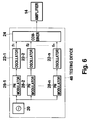
- FIG. 6 shows the configuration of a testing device 48 according to a third embodiment of the invention, wherein circuit parts identical with or similar to those previously described in the first embodiment are denoted by the same reference numerals.
- PN modulators 28-1, 28-2, ..., 28-n which are located preceding oscillators 22-1, 22-2, ..., 22-n, PN modulate oscillation output of the reference oscillator 20 with different PN code series and supply the PN modulated signals to their corresponding oscillators 22-1, 22-2, ..., 22-n.
- the third embodiment also produces an effect similar to that of the first embodiment.
- n of n waves of carriers may be any integer of 2 or greater, such as eight, 16, or 24.
- carrier frequencies are not limited; for example, frequencies in VHF and UHF bands can be used as carriers.
- means for giving phase fluctuation is not limited.
- Phase modulation mentioned in the specification shall contain frequency modulation.
- phase fluctuation is applied by frequency or phase modulation
- a modulation system other than the PN modulation can also be used.
- the method for giving fluctuations to the division ratios is not limited to the method using PN codes, i.e. other known methods are also applicable.
- the objects to the tested are not limited to the configuration shown in Figure 2.
- the testing device of the invention is adapted to give a different phase fluctuation to each of the oscillation outputs of the oscillators, can thus prevent peaks from overlapping each other and can evaluate or test the performance of an amplifier to be tested more accurately.
- the configuration of the testing device may be simplified.
- a plurality of PN modulators (28) are provided corresponding to a plurality of oscillators (22) at stages preceding or following them, or fluctuation is given to division ratios at the oscillators (22). Since each of n carriers combined by a combiner (24) contains phase fluctuation, the possibility that the peaks will overlap each other or that the carriers having opposite phases will negate each other is very low. The peak power in signals supplied to the amplifier (14) to be tested is unlikely to vary, enabling accurate evaluation or testing.
Landscapes
- Engineering & Computer Science (AREA)
- Physics & Mathematics (AREA)
- Nonlinear Science (AREA)
- Power Engineering (AREA)
- Multimedia (AREA)
- General Engineering & Computer Science (AREA)
- General Physics & Mathematics (AREA)
- Amplifiers (AREA)
- Testing Electric Properties And Detecting Electric Faults (AREA)
Applications Claiming Priority (3)
| Application Number | Priority Date | Filing Date | Title |
|---|---|---|---|
| JP8621693 | 1993-04-13 | ||
| JP8621693 | 1993-04-13 | ||
| JP86216/93 | 1993-04-13 |
Publications (3)
| Publication Number | Publication Date |
|---|---|
| EP0620446A2 true EP0620446A2 (de) | 1994-10-19 |
| EP0620446A3 EP0620446A3 (de) | 1995-08-02 |
| EP0620446B1 EP0620446B1 (de) | 2003-07-02 |
Family
ID=13880593
Family Applications (1)
| Application Number | Title | Priority Date | Filing Date |
|---|---|---|---|
| EP94105558A Expired - Lifetime EP0620446B1 (de) | 1993-04-13 | 1994-04-11 | Einrichtung zum Testen eines Verstärkers |
Country Status (4)
| Country | Link |
|---|---|
| US (1) | US5394120A (de) |
| EP (1) | EP0620446B1 (de) |
| CA (1) | CA2120174C (de) |
| DE (1) | DE69432879T2 (de) |
Cited By (3)
| Publication number | Priority date | Publication date | Assignee | Title |
|---|---|---|---|---|
| WO2000005591A1 (en) * | 1998-07-21 | 2000-02-03 | Ifr Limited | Method of and apparatus for generating a multitone test signal |
| WO2001086804A3 (en) * | 2000-05-12 | 2002-04-18 | Jhong S Lee | Ultra-linear feedforward rf power amplifier |
| EP0962783A3 (de) * | 1998-06-05 | 2003-04-23 | Murata Manufacturing Co., Ltd. | Gerät zur Messung der elektrischen Eigenschaften von Schaltungen |
Families Citing this family (3)
| Publication number | Priority date | Publication date | Assignee | Title |
|---|---|---|---|---|
| JPH0746648A (ja) * | 1993-08-02 | 1995-02-14 | Fujitsu Ltd | 移動体通信システム |
| US5789927A (en) * | 1996-06-28 | 1998-08-04 | Spectrian | Baseband measurement of RF power amplifier distortion |
| US7126421B2 (en) * | 2003-09-23 | 2006-10-24 | Powerwave Technologies, Inc. | Method for aligning feed forward loops |
Family Cites Families (12)
| Publication number | Priority date | Publication date | Assignee | Title |
|---|---|---|---|---|
| US3711620A (en) * | 1970-01-29 | 1973-01-16 | Tokyo Shibaura Electric Co | Musical tone signal generator |
| US4028622A (en) * | 1976-06-28 | 1977-06-07 | Bell Telephone Laboratories, Incorporated | Selective intermodulation distortion measurement |
| JPS5769946A (en) * | 1980-10-21 | 1982-04-30 | Fujitsu Ltd | Failure monitor system |
| US4494238A (en) * | 1982-06-30 | 1985-01-15 | Motorola, Inc. | Multiple channel data link system |
| US4556841A (en) * | 1983-11-25 | 1985-12-03 | At&T Bell Laboratories | Measurement system for characterizing power amplifier and other device performance |
| US4924744A (en) * | 1987-08-27 | 1990-05-15 | Hudson Soft Co., Ltd. | Apparatus for generating sound through low frequency and noise modulation |
| JPH07101819B2 (ja) * | 1988-05-31 | 1995-11-01 | 日本無線株式会社 | 多周波同時増幅器における歪補償回路 |
| US4885551A (en) * | 1988-10-31 | 1989-12-05 | American Telephone And Telegraph Company At&T Bell Laboratories | Feed forward linear amplifier |
| US5038341A (en) * | 1989-12-01 | 1991-08-06 | Hughes Aircraft Company | Relay communication system |
| GB9009295D0 (en) * | 1990-04-25 | 1990-06-20 | Kenington Peter B | Apparatus and method for reducing distortion in amplification |
| US5065110A (en) * | 1990-05-02 | 1991-11-12 | Teledyne Mec | Feed-forward amplifier including phase correction |
| JPH0590844A (ja) * | 1991-09-26 | 1993-04-09 | Toshiba Corp | 歪補償器 |
-
1994
- 1994-03-25 US US08/217,878 patent/US5394120A/en not_active Expired - Lifetime
- 1994-03-29 CA CA002120174A patent/CA2120174C/en not_active Expired - Fee Related
- 1994-04-11 EP EP94105558A patent/EP0620446B1/de not_active Expired - Lifetime
- 1994-04-11 DE DE69432879T patent/DE69432879T2/de not_active Expired - Lifetime
Cited By (3)
| Publication number | Priority date | Publication date | Assignee | Title |
|---|---|---|---|---|
| EP0962783A3 (de) * | 1998-06-05 | 2003-04-23 | Murata Manufacturing Co., Ltd. | Gerät zur Messung der elektrischen Eigenschaften von Schaltungen |
| WO2000005591A1 (en) * | 1998-07-21 | 2000-02-03 | Ifr Limited | Method of and apparatus for generating a multitone test signal |
| WO2001086804A3 (en) * | 2000-05-12 | 2002-04-18 | Jhong S Lee | Ultra-linear feedforward rf power amplifier |
Also Published As
| Publication number | Publication date |
|---|---|
| CA2120174C (en) | 1996-03-19 |
| EP0620446A3 (de) | 1995-08-02 |
| DE69432879T2 (de) | 2004-01-29 |
| EP0620446B1 (de) | 2003-07-02 |
| CA2120174A1 (en) | 1994-10-14 |
| DE69432879D1 (de) | 2003-08-07 |
| US5394120A (en) | 1995-02-28 |
Similar Documents
| Publication | Publication Date | Title |
|---|---|---|
| EP0541789B1 (de) | Vorwärtsgeregeltes verstärkernetzwerk mit gewobbeltem pilotton | |
| CA2157255C (en) | Feed-forward amplifier with expanded linearity | |
| RU2099881C1 (ru) | Система связи | |
| US4893300A (en) | Technique for reducing distortion characteristics in fiber-optic links | |
| EP0110368A2 (de) | Übertragungssystem für Signalpakete | |
| US6133791A (en) | Feedforward amplifier with improved characteristics without using pilot signal | |
| EP0585421A4 (en) | High dynamic range modulation independent feed forward amplifier network | |
| WO1991003108A1 (en) | Gain/phase compensation for linear amplifier feedback loop | |
| US5394120A (en) | Device for testing an amplifier | |
| US4161733A (en) | Null steering apparatus including weight oscillation eliminating means | |
| KR100325573B1 (ko) | 광학데이타신호를변조하기위해레이저에의해사용되는전기변조신호를발생하는방법및이에적합한이퀄라이저 | |
| KR100441183B1 (ko) | 튜너및스플리터-변조기를포함하는회로장치 | |
| JP2003198273A (ja) | 増幅回路 | |
| JP2940840B2 (ja) | フィードフォワード干渉回路 | |
| JP3367735B2 (ja) | 歪み特性測定用rf装置及び歪み特性測定方法 | |
| KR101077498B1 (ko) | 증폭기를 위한 선택적 주파수 위상/지연 제어 | |
| JP2954181B1 (ja) | 単一周波数放送波中継装置 | |
| JP3017012B2 (ja) | 増幅装置の試験装置 | |
| GB2259628A (en) | Transmitter power control unit | |
| US6734727B2 (en) | Feedforward amplifier, feedforward amplification method | |
| JP2679445B2 (ja) | 送信電力制御方式 | |
| JPH01302901A (ja) | 多周波同時増幅器における歪補償回路 | |
| JP2852294B2 (ja) | 送信機 | |
| EP0944175A1 (de) | Filter für einen Mobilfunktelefon | |
| JP4612136B2 (ja) | 増幅器 |
Legal Events
| Date | Code | Title | Description |
|---|---|---|---|
| PUAI | Public reference made under article 153(3) epc to a published international application that has entered the european phase |
Free format text: ORIGINAL CODE: 0009012 |
|
| AK | Designated contracting states |
Kind code of ref document: A2 Designated state(s): DE FR GB NL SE |
|
| PUAL | Search report despatched |
Free format text: ORIGINAL CODE: 0009013 |
|
| AK | Designated contracting states |
Kind code of ref document: A3 Designated state(s): DE FR GB NL SE |
|
| 17P | Request for examination filed |
Effective date: 19950817 |
|
| 17Q | First examination report despatched |
Effective date: 20000131 |
|
| GRAH | Despatch of communication of intention to grant a patent |
Free format text: ORIGINAL CODE: EPIDOS IGRA |
|
| GRAH | Despatch of communication of intention to grant a patent |
Free format text: ORIGINAL CODE: EPIDOS IGRA |
|
| GRAA | (expected) grant |
Free format text: ORIGINAL CODE: 0009210 |
|
| RAP1 | Party data changed (applicant data changed or rights of an application transferred) |
Owner name: NTT DOCOMO, INC. Owner name: JAPAN RADIO CO., LTD |
|
| AK | Designated contracting states |
Designated state(s): DE FR GB NL SE |
|
| REG | Reference to a national code |
Ref country code: GB Ref legal event code: FG4D |
|
| REG | Reference to a national code |
Ref country code: SE Ref legal event code: TRGR |
|
| REF | Corresponds to: |
Ref document number: 69432879 Country of ref document: DE Date of ref document: 20030807 Kind code of ref document: P |
|
| ET | Fr: translation filed | ||
| PLBE | No opposition filed within time limit |
Free format text: ORIGINAL CODE: 0009261 |
|
| STAA | Information on the status of an ep patent application or granted ep patent |
Free format text: STATUS: NO OPPOSITION FILED WITHIN TIME LIMIT |
|
| 26N | No opposition filed |
Effective date: 20040405 |
|
| PGFP | Annual fee paid to national office [announced via postgrant information from national office to epo] |
Ref country code: GB Payment date: 20100325 Year of fee payment: 17 |
|
| PGFP | Annual fee paid to national office [announced via postgrant information from national office to epo] |
Ref country code: FR Payment date: 20100521 Year of fee payment: 17 |
|
| PGFP | Annual fee paid to national office [announced via postgrant information from national office to epo] |
Ref country code: NL Payment date: 20100416 Year of fee payment: 17 Ref country code: DE Payment date: 20100430 Year of fee payment: 17 |
|
| PGFP | Annual fee paid to national office [announced via postgrant information from national office to epo] |
Ref country code: SE Payment date: 20100409 Year of fee payment: 17 |
|
| REG | Reference to a national code |
Ref country code: DE Ref legal event code: R119 Ref document number: 69432879 Country of ref document: DE |
|
| REG | Reference to a national code |
Ref country code: DE Ref legal event code: R119 Ref document number: 69432879 Country of ref document: DE |
|
| REG | Reference to a national code |
Ref country code: NL Ref legal event code: V1 Effective date: 20111101 |
|
| REG | Reference to a national code |
Ref country code: SE Ref legal event code: EUG |
|
| GBPC | Gb: european patent ceased through non-payment of renewal fee |
Effective date: 20110411 |
|
| REG | Reference to a national code |
Ref country code: FR Ref legal event code: ST Effective date: 20111230 |
|
| PG25 | Lapsed in a contracting state [announced via postgrant information from national office to epo] |
Ref country code: FR Free format text: LAPSE BECAUSE OF NON-PAYMENT OF DUE FEES Effective date: 20110502 Ref country code: NL Free format text: LAPSE BECAUSE OF NON-PAYMENT OF DUE FEES Effective date: 20111101 |
|
| PG25 | Lapsed in a contracting state [announced via postgrant information from national office to epo] |
Ref country code: GB Free format text: LAPSE BECAUSE OF NON-PAYMENT OF DUE FEES Effective date: 20110411 |
|
| PG25 | Lapsed in a contracting state [announced via postgrant information from national office to epo] |
Ref country code: SE Free format text: LAPSE BECAUSE OF NON-PAYMENT OF DUE FEES Effective date: 20110412 |
|
| PG25 | Lapsed in a contracting state [announced via postgrant information from national office to epo] |
Ref country code: DE Free format text: LAPSE BECAUSE OF NON-PAYMENT OF DUE FEES Effective date: 20111031 |