EP0620650A2 - Schnittstelleschaltung - Google Patents
Schnittstelleschaltung Download PDFInfo
- Publication number
- EP0620650A2 EP0620650A2 EP94105622A EP94105622A EP0620650A2 EP 0620650 A2 EP0620650 A2 EP 0620650A2 EP 94105622 A EP94105622 A EP 94105622A EP 94105622 A EP94105622 A EP 94105622A EP 0620650 A2 EP0620650 A2 EP 0620650A2
- Authority
- EP
- European Patent Office
- Prior art keywords
- mos transistor
- backgate
- circuit
- output
- current path
- Prior art date
- Legal status (The legal status is an assumption and is not a legal conclusion. Google has not performed a legal analysis and makes no representation as to the accuracy of the status listed.)
- Granted
Links
Images


Classifications
-
- H—ELECTRICITY
- H03—ELECTRONIC CIRCUITRY
- H03K—PULSE TECHNIQUE
- H03K19/00—Logic circuits, i.e. having at least two inputs acting on one output; Inverting circuits
-
- H—ELECTRICITY
- H03—ELECTRONIC CIRCUITRY
- H03K—PULSE TECHNIQUE
- H03K19/00—Logic circuits, i.e. having at least two inputs acting on one output; Inverting circuits
- H03K19/0175—Coupling arrangements; Interface arrangements
- H03K19/0185—Coupling arrangements; Interface arrangements using field effect transistors only
- H03K19/018507—Interface arrangements
-
- H—ELECTRICITY
- H03—ELECTRONIC CIRCUITRY
- H03K—PULSE TECHNIQUE
- H03K19/00—Logic circuits, i.e. having at least two inputs acting on one output; Inverting circuits
- H03K19/0175—Coupling arrangements; Interface arrangements
- H03K19/0185—Coupling arrangements; Interface arrangements using field effect transistors only
- H03K19/018507—Interface arrangements
- H03K19/018521—Interface arrangements of complementary type, e.g. CMOS
-
- H—ELECTRICITY
- H03—ELECTRONIC CIRCUITRY
- H03K—PULSE TECHNIQUE
- H03K2217/00—Indexing scheme related to electronic switching or gating, i.e. not by contact-making or -breaking covered by H03K17/00
- H03K2217/0018—Special modifications or use of the back gate voltage of a FET
Definitions
- This invention relates to an interface circuit in a semiconductor integrated circuit (IC), and more particularly to an interface circuit serving as an interface between a circuit of high power supply voltage system and a circuit of low power supply voltage system which commonly use a bus line.
- IC semiconductor integrated circuit
- semiconductor elements formed based on the 0.8 micron design rule are operated on a power supply voltage of 5V.
- semiconductor elements formed by the fine pattern technology based on the 0.5 micron design rule for example, are operated on a power supply voltage of 3.3V or 3.0V since the gate oxide film thereof is made thin and the withstanding voltage thereof is lowered (generally, it is estimated to be 3.6V).
- FIG. 1 schematically shows the construction of a circuit in which an IC of low power supply voltage (for example, 3.3V) system and an IC of high power supply voltage (for example, 5V) system commonly use a bus line.
- An IC 91 of 3.3V system and ICs 92-1, 92-2 of 5V system are connected together via a bus line 93.
- an output circuit 91a operated on a power supply voltage of 3.3V is provided
- an output circuit 92a operated on a power supply voltage of 5V is provided.
- the output circuits 91a, 92a are supplied with output enable signals OE ⁇ , OE respectively and the output states thereof are controlled.
- an input circuit 92b operated on a power supply voltage of 5V is provided.
- FIG. 2 shows an example of the construction of an output stage in the output circuit 91a of the IC 91 of 3.3V system in the circuit shown in FIG. 1.
- the circuit is constructed by a P-channel MOS transistor (which is hereinafter referred to as a PMOS transistor) P1, N-channel MOS transistor (which is hereinafter referred to as an NMOS transistor) N1, and depletion type NMOS transistor N2.
- the gate potentials of the MOS transistors P1, N1 are selectively controlled by an output signal from the internal circuit, the output node Na is selectively set to one of the "H" level, "L” level and high impedance state, and thus they function as a tri-state buffer.
- the NMOS transistor N2 whose source-drain path is connected between the output node Na and an output terminal Nb of the IC 91 functions to separate the output node Na of the tri-state buffer from the IC 92-1 of 5V system, the gate thereof is connected to the power supply Vcc and the backgate thereof is fixed at the ground potential Vss.
- the NMOS transistor N2 outputs a voltage near the power supply voltage Vcc to the output terminal Nb when the potential of the output node Na of the tri-state buffer is set at the "H" level. Therefore, if the threshold voltage of the NMOS transistor N2 is always kept at 0V, a voltage of 3.3V is output from the output node Nb of the IC 91.
- the threshold voltage of the depletion type NMOS transistor by taking the backgate bias effect into consideration so as to satisfy the above two limitations, that is, the limitation that the power supply voltage Vcc is output from the output terminal Nb of the IC 91 when the potential of the node Na is at the "H" level and the limitation that the potential of the node Na is suppressed within the permitted voltage range if 5V is applied to the output terminal Nb of the IC 91 via the bus line when the node Na is set at the high impedance state.
- the threshold voltage Vthn2 of the NMOS transistor N2 is considered.
- the potential of the node Na is pulled by the applied voltage and rises.
- the potential of the node Na must not be set equal to or higher than 3.6V.
- the threshold voltage Vthn2 of the NMOS transistor N2 must be set within a range between the one-dot-dash line Lc and the two-dot-dash line Ld in FIG. 3 and the margin of the threshold voltage Vthn2 set at this time is 0.48V.
- the output circuit of the conventional IC shown in FIG. 2 has a disadvantage that the operation margin for a variation in the threshold voltage Vthn2 of the depletion type NMOS transistor N2 inserted for separation of the output node Na of the tri-state buffer from the bus line 93 is small and the process control is difficult.
- a third object of this invention is to provide an interface circuit provided in the output stage of a circuit of low power supply voltage system formed in a semiconductor substrate and capable of enlarging the operation margin for a variation of the threshold voltage of a MOS transistor for separation from a circuit of high power supply voltage and simplifying the process control.
- a backgate bias can be selectively applied to the first MOS transistor by controlling the first and second switching elements according to the operation mode of the first MOS transistor. That is, if a signal of high power supply voltage system is supplied to the output terminal of the IC via the bus line of the exterior of the IC when the output node of the MOS circuit (for example, an output buffer circuit of the IC) is set in the high impedance state, the threshold voltage of the first MOS transistor is raised to a maximum by most effectively utilizing the backgate bias effect of the first MOS transistor in the operation mode in which a signal of high power supply voltage system is transmitted to the output node of the MOS circuit via the current path of the first MOS transistor so as to increase the transmitted signal voltage drop and suppress the potential of the output node of the MOS circuit to a preset value or less.
- the backgate bias effect of the first MOS transistor is suppressed to a minimum so as to lower the threshold voltage of the first MOS transistor and reduce the output signal voltage drop to be transmitted.
- a state in which the backgate bias effect of the first MOS transistor is suppressed to a minimum so as to set up the same state as the normal "L" level transmission state.
- the permissible range of the variations in the threshold voltages of the first and second MOS transistors can be enlarged and the operation margin for the variation in the threshold voltages can be significantly increased even if the process fluctuation and temperature dependency are taken into consideration.
- the process control can be simplified.
- the fourth object of this invention can be attained by an output circuit comprising a MOS circuit formed in a semiconductor substrate and including a first MOS transistor and a second MOS transistor whose current paths are series-connected between a first potential supplying source and a second potential supplying source; a third MOS transistor of a first conductivity type having a current path connected at one end to a connection node between the first and second MOS transistors and connected at the other end to an output terminal and a gate connected to the first potential supplying source; a first switching element connected between a backgate of the third MOS transistor and the second potential supplying source; a fourth MOS transistor of the first conductivity type having a current path connected at one end to the output terminal, a gate connected to the first potential supplying source and a backgate set at the same potential as that of the backgate of the third MOS transistor; and a second switching element connected between the other end of the current path of the fourth MOS transistor and the backgate of the third MOS transistor, the ON/OFF state thereof being controlled in
- FIG. 4 is a circuit diagram showing a basic construction of an interface circuit according to a first embodiment of this invention.
- This interface circuit is formed in a semiconductor substrate and includes a MOS circuit 11, first NMOS transistor T1 of depletion type, first switching element SW1, second switching element SW2, second NMOS transistor T2 of depletion type, and control circuit 12.
- An input node of the MOS circuit 11 is connected to an input terminal Ne.
- the source-drain path of the NMOS transistor T1 is connected between an output node Na of the MOS circuit 11 and an output terminal Nb and the gate thereof is connected to a first potential supplying source (for example, power supply Vcc).
- a first potential supplying source for example, power supply Vcc
- the switching element SW1 is inserted between the backgate (substrate region) of the NMOS transistor T1 and a second potential supplying source (for example, ground terminal Vss).
- a second potential supplying source for example, ground terminal Vss.
- One end of the current path of the NMOS transistor T2 is connected to the output terminal Nb, the gate thereof is connected to the power supply Vcc, and the backgate thereof is set at the same potential as that of the backgate of the NMOS transistor T1.
- the switching element SW2 is connected between the other end of the current path of the NMOS transistor T2 and the backgate of the NMOS transistor T1 and the ON/OFF state thereof is controlled in a complementary state with respect to that of the switching element SW1.
- the control circuit 12 generates a control signal in response to a signal input from the input terminal Ne to control the MOS circuit 11, first switching element SW1 and second switching element SW2. As shown by broken lines in FIG. 4, the control circuit 12 and MOS circuit 11 may be sometimes controlled by another control signal (for example, an output enable signal OE ⁇ ) supplied from the exterior.
- another control signal for example, an output enable signal OE ⁇
- a backgate bias is selectively applied to the NMOS transistor T1 by controlling the ON/OFF state of the first and second switching elements SW1 and SW2 by the control circuit 12 according to the the operation mode of the NMOS transistor T1. That is, when the output node Na of the MOS circuit 11 is set in the high impedance state, a signal is supplied from a circuit of high power supply voltage system to the output terminal Nb, and when the NMOS transistor T1 is set in the operation mode for transmitting the signal to the output node Na of the MOS circuit 11, the backgate bias effect of the NMOS transistor T1 is set to a maximum by turning ON the switching element SW1 and turning OFF the switching element SW2.
- a state in which substantially no backgate bias effect of the NMOS transistor T1 occurs (a state in which substantially no difference occurs between the substrate bias and the source potential occurs) is set up, and thus, substantially the same state as that set up at the time of normal transmission of "L" level is set up.
- the permissible range of variations in the threshold voltages of the first and second MOS transistors can be enlarged and the operation margin for the variation in the threshold voltage can be significantly increased.
- the process control can be simplified.
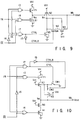
- FIG. 5 illustrates an interface circuit according to a second embodiment of this invention in which the interface circuit shown in FIG. 4 is provided in the output circuit of the IC.
- the IC having the interface circuit formed therein is operated on a low power supply voltage (for example, 3.3V or 3V) system.
- the IC is connected to an IC of high power supply voltage (for example, 5V) system via a bus line and the reference potentials (ground potential Vss) thereof are the same.
- the interface circuit is formed in an N-type semiconductor substrate.
- a P well region, the source and drain regions of a PMOS transistor are formed in the substrate, and the source and drain regions of an NMOS transistor are formed in the P well region. Assume that the substrate is biased to the power supply potential Vcc and the P well region is biased to the ground potential Vss if no special explanation is made.
- the output buffer circuit includes a PMOS transistor P1 and an NMOS transistor N1 serially connected between the power supply Vcc and the ground terminal Vss.
- the MOS transistors P1, N1 are controlled such that the output node Na will be set to the "H” level, "L” level or high impedance state by controlling the gate potentials thereof according to outputs of the NAND gate 13 and NOR gate 14 and thus construct a tri-state buffer circuit.
- the source-drain path of a first NMOS transistor N2 of depletion type is connected between the output node Na of the tri-state buffer circuit and the output terminal Nb of the IC and the gate thereof is connected to the power supply Vcc.
- a first switching element SW1 is inserted between the backgate (node Nc) of the first MOS transistor N2 and the ground terminal Vss.
- a second switching element SW2 and the source-drain path of a second NMOS transistor N3 of depletion type are series-connected between the backgate of the NMOS transistor N2 and the output terminal Nb of the IC.
- the ON/OFF state of the switching element SW2 is controlled in a complementary state with respect to that of the switching element SW1.
- the second NMOS transistor N3 has a gate connected to the power supply Vcc and the backgate thereof is connected with the backgate of the NMOS transistor N2, for example, so as to be set at the same potential as that of the backgate of the NMOS transistor N2.
- a control signal CTRL is a 3.3V system signal and the ON/OFF state of the switching element SW1 is controlled according to the "H"/"L" level of the signal. Further, the ON/OFF state of the switching element SW2 is controlled according to the "L"/"H" level of control signals CTRL CTRLB.
- NMOS transistor As the first switching element SW1, a normally-OFF type NMOS transistor is used, for example, and the backgate thereof is connected to the ground terminal Vss.
- the second switching element SW2 an analog switch constructed by a PMOS transistor P4 and an NMOS transistor N4 whose current paths are connected in parallel with each other is used.
- the gates of the MOS transistors P4, N4 are controlled by the control signals CTRL, CTRLB respectively.
- the backgate of the NMOS transistor N4 is connected to the ground terminal Vss.
- an output enable control signal OE ⁇ and an input signal from the internal circuit are used.
- the signals IN and OE ⁇ are supplied to a 2-input NOR gate 14 whose output is supplied to the gate of the NMOS transistor N1.
- the signal OE ⁇ is inverted by an inverter 16 and an inverted signal OE and the input signal IN are supplied to a 2-input NAND gate 13.
- An output of the NAND gate 13 is supplied to the gate of the PMOS transistor P1.
- the signals OE and IN are supplied to a 2-input NAND gate 17 whose output is supplied to the gates of the MOS transistors N5, P4 as the signal CTRL. Further, the signal CTRL is inverted by an inverter 15 and then supplied to the gate of the NMOS transistors N4 as the control signal CTRLB.
- the threshold voltage Vthn2 of the NMOS transistor N2 can be increased to the maximum possible value by most effectively using the backgate bias effect of the NMOS transistor N2 and the voltage drop of a signal to be transmitted is increased so that the potential of the output node Na of the tri-state buffer can be suppressed to a potential level equal to or lower than the breakdown voltage of the MOS transistor N1.
- the threshold voltage Vthn3 of the NMOS transistor N3 is set to be not higher than a preset value, the potential difference between Vd and the gate potential (in this example, ground potential Vss) of the NMOS transistor N4 constituting the switching element SW2 can be set equal to or less than 3.6V (maximum breakdown voltage).
- the threshold voltages Vthn2, Vthn3 of the NMOS transistor N2, N3 are considered.
- the potential of the node Na is raised by the applied voltage, but in this case, the potential of the node Na must be prevented from being set equal to or higher than 3.6V when taking the withstanding voltage between the gate and drain of the NMOS transistor N1 into consideration.
- the potential Va of the node Na is controlled by the gate potential V G2 of the NMOS transistor N2. That is, it is raised to a potential which satisfies the following relation.
- the margins for the threshold voltages Vthn2, Vthn3 of the NMOS transistors N2, N3 set when the IC having the output circuit of FIG. 5 is operated on the 3V system power supply voltage are considered.
- the range of the 3V system power supply voltage is 3.0V ⁇ 0.3V
- the maximum value of the gate withstanding voltage of the element is 3.6V
- the range of a 5V system signal supplied to the bus line is 5.0V ⁇ 0.5V.
- the switching elements SW1, SW2 are respectively set in the OFF and ON states.
- the backgate (node Nc) of the NMOS transistor N2 is separated from the ground terminal Vss.
- the potential of the node Nd of one end (which lies on the second switching element SW2 side) of the current path of the NMOS transistor N3 is set to the same potential of the node Nc.
- the potential Vc of the node Nc, the potential Vd of the node Nd and the output voltage Vout are raised to values as indicated by the following equations.
- the NMOS transistor N2 may reduce the voltage drop of a signal to be transmitted and the output voltage Vout can be set to a level higher than the conventional case since the backgate bias effect of the first NMOS transistor is smaller than the conventional case (the substrate bias potential
- the threshold voltages Vthn2, Vthn3 of the NMOS transistors N2, N3 in the second operation mode are considered.
- the range of the 3.3V system power supply voltage is 3.3V ⁇ 0.3V
- the maximum value of the gate withstanding voltage of the element is 3.6V
- the range of a 5V system signal supplied to the bus line is 5.0V ⁇ 0.5V.
- the output voltage Vout of the IC must be stably set to be 2.7V or more in this operation mode. This stable setting becomes severest in the case of minimum power supply voltage level (3V) of 3.3V system. Further, assume that the characteristics (threshold voltages, backgate bias effects) of the NMOS transistors N2, N3 are set equal to each other.
- Vout Vcc - Vthn0
- Vthn0 must be set within a range of 0.3 ⁇ Vthn0.
- the threshold voltages Vthn2, Vthn3 vary by 0.3V for a variation of -1V in the substrate bias voltage V BS as the backgate bias effect, it becomes necessary to set the threshold voltages Vthn2, Vthn3 of the NMOS transistors in a region lying below the solid line La indicated in FIG. 6. Therefore, in the 3.3V system, the threshold voltages Vthn2, Vthn3 must be set in a range between the solid lines La and Lb shown in FIG. 6, the margin is 1.38V and is thus increased by 0.81V in comparison with the margin of 0.57V of the conventional case shown in FIG. 3.
- the margins of the threshold voltages Vthn2, Vthn3 of the NMOS transistors N2, N3 set when the IC having the output circuit of FIG. 5 is operated on the 3V power supply voltage system are considered.
- the range of the 3V power supply voltage system is 3.0V ⁇ 0.3V
- the maximum value of the gate withstanding voltage of the element is 3.6V
- the range of a 5V system signal to be supplied to the bus line is 5.0V ⁇ 0.5V.
- the threshold voltages Vthn2, Vthn3 must lie in a region between the one-dot-dash line Lc and the two-dot-dash line Ld shown in FIG. 6, and the margin is set to 1.29V and increased by 0.81V in comparison with the margin of 0.48V of the conventional interface circuit shown in FIG. 3.
- the node Nc is connected to the ground terminal Vss and the node Nd is separated from the node Nc by controlling the first and second switching elements SW1, SW2 into the ON and OFF states, respectively.
- the switching elements SW1, SW2 are controlled according to the operation mode of the NMOS transistor N2 so as to control the bias of the backgate (P well region) of the NMOS transistor N2, it becomes possible to effectively apply a backgate bias to the NMOS transistor N2.
- the permissible range of variations in the threshold voltages Vthn2, Vthn3 of the NMOS transistors N2, N3 can be enlarged even when taking the process fluctuation and temperature dependency (-2 to 3 mV/°C) into consideration.
- the operation margin for the variation in the threshold voltage can be increased twice as large as that of the conventional case and the process control can be simplified.
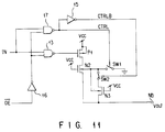
- An output circuit shown in FIG. 7 is different from the output circuit shown in FIG. 5 in that only a normally OFF type NMOS transistor N4 is used as the switching element SW2 and the backgate of the NMOS transistor N4 is connected to the ground terminal Vss.
- the other construction is the same and like portions are denoted by the same reference numerals as those shown in FIG. 5.
- the operation of the output circuit is basically the same as the operation of the output circuit of FIG. 5, but the potentials of the nodes Nc, Nd in the second operation mode in which the "H" level of the output node Na of the tri-state buffer is transmitted to the output terminal Nb of the IC are somewhat different.
- Vc Vcc - Vth4 (at the time of Vth4 > Vth3)
- Vc Vcc - Vth3 (at the time of Vth3 ⁇ Vth4)
- Vth3 ⁇ Vth4 the circuit condition is the same as that set in the case wherein no voltage drop occurs in the MOS transistors N4 and P4 of FIG. 5 and no voltage drop occurs in the switching element SW2.
- the circuit condition corresponds to that set in the case where a voltage drop occurs in the switching element SW2 of FIG. 5. If the threshold voltage Vth4 is adequately selected, a rise in the threshold voltage due to the backgate bias effect is made smaller than that in the conventional case in which the potential of the backgate (substrate region) of the first NMOS transistor N2 is fixed at the ground potential Vss so that the output voltage Vout will be set to a higher level than in the conventional case.
- the margins of the threshold voltages Vthn2, Vthn3, Vthn4 in the second operation mode are considered.
- the characteristics (threshold voltages, backgate bias effects) of the first NMOS transistor N2 and the second NMOS transistor N3 and third NMOS transistor N4 are set equal to each other.
- Vout, Vc, Vd can be raised until the following relations are satisfied.
- Vc (Vcc - Vthn0)/1.3
- Vd (Vcc - Vthn0) ⁇ 1.6/1.69
- Vcc (Vcc - Vthn0) ⁇ 1.6/1.69
- Vd ⁇ 2.7V the relation of Vd ⁇ 2.7V must be satisfied. At this time, it is necessary to set the threshold voltage Vthn0 within the range of -0.152 ⁇ Vthn0. In this case, Vc ⁇ 2.194V.
Landscapes
- Engineering & Computer Science (AREA)
- Computer Hardware Design (AREA)
- Physics & Mathematics (AREA)
- Computing Systems (AREA)
- General Engineering & Computer Science (AREA)
- Mathematical Physics (AREA)
- Logic Circuits (AREA)
- Dram (AREA)
Applications Claiming Priority (2)
| Application Number | Priority Date | Filing Date | Title |
|---|---|---|---|
| JP5084507A JP2888722B2 (ja) | 1993-04-12 | 1993-04-12 | インターフェース回路 |
| JP84507/93 | 1993-04-12 |
Publications (3)
| Publication Number | Publication Date |
|---|---|
| EP0620650A2 true EP0620650A2 (de) | 1994-10-19 |
| EP0620650A3 EP0620650A3 (de) | 1995-07-12 |
| EP0620650B1 EP0620650B1 (de) | 1997-08-06 |
Family
ID=13832564
Family Applications (1)
| Application Number | Title | Priority Date | Filing Date |
|---|---|---|---|
| EP94105622A Expired - Lifetime EP0620650B1 (de) | 1993-04-12 | 1994-04-12 | Schnittstellenschaltung |
Country Status (5)
| Country | Link |
|---|---|
| US (1) | US5442307A (de) |
| EP (1) | EP0620650B1 (de) |
| JP (1) | JP2888722B2 (de) |
| KR (1) | KR0136233B1 (de) |
| DE (1) | DE69404726T2 (de) |
Cited By (2)
| Publication number | Priority date | Publication date | Assignee | Title |
|---|---|---|---|---|
| EP0668658A3 (de) * | 1994-02-16 | 1997-04-09 | Toshiba Kk | Ausgangsschaltung zur Verwendung in einer integrierten Halbleiterschaltung. |
| US6084431A (en) * | 1995-12-26 | 2000-07-04 | Kabushiki Kaisha Toshiba | Output circuit providing protection against external voltages in excess of power-supply voltage |
Families Citing this family (22)
| Publication number | Priority date | Publication date | Assignee | Title |
|---|---|---|---|---|
| US5694075A (en) * | 1994-12-30 | 1997-12-02 | Maxim Integrated Products | Substrate clamp for non-isolated integrated circuits |
| US5675809A (en) * | 1995-02-10 | 1997-10-07 | Ncr Corporation | Voltage control circuit for a dual voltage bus computer system |
| JP3441238B2 (ja) | 1995-06-02 | 2003-08-25 | 株式会社東芝 | 出力回路 |
| JP2827963B2 (ja) * | 1995-06-02 | 1998-11-25 | 日本電気株式会社 | 半導体集積回路装置 |
| US5543733A (en) * | 1995-06-26 | 1996-08-06 | Vlsi Technology, Inc. | High voltage tolerant CMOS input/output circuit |
| FR2738424B1 (fr) * | 1995-09-05 | 1997-11-21 | Sgs Thomson Microelectronics | Interrupteur analogique basse tension |
| US5808956A (en) * | 1995-12-20 | 1998-09-15 | Seiko Epson Corporation | Bus-line drive circuit and semiconductor storage device comprising the same |
| JPH09293789A (ja) * | 1996-04-24 | 1997-11-11 | Mitsubishi Electric Corp | 半導体集積回路 |
| US5844425A (en) * | 1996-07-19 | 1998-12-01 | Quality Semiconductor, Inc. | CMOS tristate output buffer with having overvoltage protection and increased stability against bus voltage variations |
| JP3437719B2 (ja) * | 1996-07-24 | 2003-08-18 | 株式会社東芝 | アナログ・スイッチ回路 |
| US5818099A (en) * | 1996-10-03 | 1998-10-06 | International Business Machines Corporation | MOS high frequency switch circuit using a variable well bias |
| TW382670B (en) * | 1996-11-21 | 2000-02-21 | Hitachi Ltd | Low power processor |
| JP3746273B2 (ja) * | 2003-02-12 | 2006-02-15 | 株式会社東芝 | 信号レベル変換回路 |
| JP3984222B2 (ja) * | 2003-12-15 | 2007-10-03 | 株式会社東芝 | 信号レベル変換回路 |
| JP2006071763A (ja) * | 2004-08-31 | 2006-03-16 | Fuji Photo Film Co Ltd | 科学現象の評価装置、及びその装置を使用した科学現象の評価方法 |
| JP4188933B2 (ja) | 2005-03-29 | 2008-12-03 | 富士通マイクロエレクトロニクス株式会社 | トレラント入力回路 |
| JP2006301840A (ja) * | 2005-04-19 | 2006-11-02 | Toshiba Corp | 信号レベル変換バススイッチ |
| US7567094B2 (en) * | 2006-06-14 | 2009-07-28 | Lightwire Inc. | Tri-stated driver for bandwidth-limited load |
| US7826275B2 (en) * | 2007-12-10 | 2010-11-02 | Macronix International Co., Ltd. | Memory circuit with high reading speed and low switching noise |
| US10044354B2 (en) * | 2016-07-11 | 2018-08-07 | Ricoh Company, Ltd. | I/O cell |
| KR102037903B1 (ko) | 2019-08-01 | 2019-10-29 | 주식회사 블럭나인 | 트로이덜 코일 권선장치 |
| CN119788058B (zh) * | 2025-03-12 | 2025-06-24 | 上海芯炽集成电路技术有限公司 | 一种电平转换电路 |
Family Cites Families (6)
| Publication number | Priority date | Publication date | Assignee | Title |
|---|---|---|---|---|
| US3720848A (en) * | 1971-07-01 | 1973-03-13 | Motorola Inc | Solid-state relay |
| DE3226339C2 (de) * | 1981-07-17 | 1985-12-19 | Tokyo Shibaura Denki K.K., Kawasaki, Kanagawa | Analoge Schaltervorrichtung mit MOS-Transistoren |
| DE3729926A1 (de) * | 1987-09-07 | 1989-03-23 | Siemens Ag | Cmos-ausgangsstufe |
| JPH057149A (ja) * | 1991-06-27 | 1993-01-14 | Fujitsu Ltd | 出力回路 |
| JP3321188B2 (ja) * | 1991-07-26 | 2002-09-03 | 株式会社東芝 | 出力回路 |
| US5191244A (en) * | 1991-09-16 | 1993-03-02 | Advanced Micro Devices, Inc. | N-channel pull-up transistor with reduced body effect |
-
1993
- 1993-04-12 JP JP5084507A patent/JP2888722B2/ja not_active Expired - Fee Related
-
1994
- 1994-04-12 KR KR1019940007572A patent/KR0136233B1/ko not_active Expired - Fee Related
- 1994-04-12 DE DE69404726T patent/DE69404726T2/de not_active Expired - Fee Related
- 1994-04-12 US US08/226,683 patent/US5442307A/en not_active Expired - Fee Related
- 1994-04-12 EP EP94105622A patent/EP0620650B1/de not_active Expired - Lifetime
Cited By (3)
| Publication number | Priority date | Publication date | Assignee | Title |
|---|---|---|---|---|
| EP0668658A3 (de) * | 1994-02-16 | 1997-04-09 | Toshiba Kk | Ausgangsschaltung zur Verwendung in einer integrierten Halbleiterschaltung. |
| US5661414A (en) * | 1994-02-16 | 1997-08-26 | Kabushiki Kaisha Toshiba | Output circuit for use in a semiconductor integrated circuit |
| US6084431A (en) * | 1995-12-26 | 2000-07-04 | Kabushiki Kaisha Toshiba | Output circuit providing protection against external voltages in excess of power-supply voltage |
Also Published As
| Publication number | Publication date |
|---|---|
| JP2888722B2 (ja) | 1999-05-10 |
| KR0136233B1 (ko) | 1998-05-15 |
| JPH06303126A (ja) | 1994-10-28 |
| EP0620650B1 (de) | 1997-08-06 |
| EP0620650A3 (de) | 1995-07-12 |
| DE69404726D1 (de) | 1997-09-11 |
| DE69404726T2 (de) | 1998-03-19 |
| US5442307A (en) | 1995-08-15 |
| KR940025179A (ko) | 1994-11-19 |
Similar Documents
| Publication | Publication Date | Title |
|---|---|---|
| EP0620650B1 (de) | Schnittstellenschaltung | |
| US5880620A (en) | Pass gate circuit with body bias control | |
| US6169443B1 (en) | Transmission gate | |
| US5160855A (en) | Floating-well CMOS output driver | |
| US5926056A (en) | Voltage tolerant output buffer | |
| EP0614279A2 (de) | Überspannungstolerante Ausgangspufferschaltung | |
| US5764077A (en) | 5 volt tolerant I/O buffer circuit | |
| US5434526A (en) | Output circuit and semiconductor integrated circuit device | |
| EP0788684A1 (de) | Hochspannungspegelschieber zum schalten von hohen spannungen in integrierten nichtflüchtigen speicherschaltungen | |
| US5973544A (en) | Intermediate potential generation circuit | |
| US6046622A (en) | Electronic analogue switch | |
| US6441651B2 (en) | High voltage tolerable input buffer | |
| US5371419A (en) | CMOS well switching circuit | |
| KR100334365B1 (ko) | 시모스 입력 버퍼 보호 회로 | |
| US5963083A (en) | CMOS reference voltage generator | |
| KR100691349B1 (ko) | 멀티 파워 시스템에 사용되는 차동 회로, 출력 버퍼 회로및 반도체 집적 회로 | |
| JP4609884B2 (ja) | 半導体集積回路装置 | |
| EP0829966B1 (de) | Ausgangsschaltung | |
| US6329841B1 (en) | Level-shifter for extremely low power supply | |
| KR100300687B1 (ko) | 반도체집적회로 | |
| US5952866A (en) | CMOS output buffer protection circuit | |
| EP0365331A1 (de) | ECL/CMOS-Pegelwandler | |
| KR100240131B1 (ko) | 씨엠오에스(cmos)회로의 래치업 저감출력드라이버 및 래치 업 저감방법 | |
| CN118157656A (zh) | 具有gidl电流减小的电平移位器 | |
| US6545506B1 (en) | CMOS output driver that can tolerant a high input voltage |
Legal Events
| Date | Code | Title | Description |
|---|---|---|---|
| PUAI | Public reference made under article 153(3) epc to a published international application that has entered the european phase |
Free format text: ORIGINAL CODE: 0009012 |
|
| 17P | Request for examination filed |
Effective date: 19940412 |
|
| AK | Designated contracting states |
Kind code of ref document: A2 Designated state(s): DE FR GB |
|
| PUAL | Search report despatched |
Free format text: ORIGINAL CODE: 0009013 |
|
| AK | Designated contracting states |
Kind code of ref document: A3 Designated state(s): DE FR GB |
|
| GRAG | Despatch of communication of intention to grant |
Free format text: ORIGINAL CODE: EPIDOS AGRA |
|
| 17Q | First examination report despatched |
Effective date: 19961217 |
|
| GRAH | Despatch of communication of intention to grant a patent |
Free format text: ORIGINAL CODE: EPIDOS IGRA |
|
| GRAH | Despatch of communication of intention to grant a patent |
Free format text: ORIGINAL CODE: EPIDOS IGRA |
|
| GRAA | (expected) grant |
Free format text: ORIGINAL CODE: 0009210 |
|
| AK | Designated contracting states |
Kind code of ref document: B1 Designated state(s): DE FR GB |
|
| PG25 | Lapsed in a contracting state [announced via postgrant information from national office to epo] |
Ref country code: FR Free format text: THE PATENT HAS BEEN ANNULLED BY A DECISION OF A NATIONAL AUTHORITY Effective date: 19970806 |
|
| REF | Corresponds to: |
Ref document number: 69404726 Country of ref document: DE Date of ref document: 19970911 |
|
| ET | Fr: translation filed | ||
| PG25 | Lapsed in a contracting state [announced via postgrant information from national office to epo] |
Ref country code: GB Free format text: LAPSE BECAUSE OF NON-PAYMENT OF DUE FEES Effective date: 19980412 |
|
| PLBE | No opposition filed within time limit |
Free format text: ORIGINAL CODE: 0009261 |
|
| STAA | Information on the status of an ep patent application or granted ep patent |
Free format text: STATUS: NO OPPOSITION FILED WITHIN TIME LIMIT |
|
| 26N | No opposition filed | ||
| GBPC | Gb: european patent ceased through non-payment of renewal fee |
Effective date: 19980412 |
|
| REG | Reference to a national code |
Ref country code: FR Ref legal event code: ST |
|
| PGFP | Annual fee paid to national office [announced via postgrant information from national office to epo] |
Ref country code: DE Payment date: 20060406 Year of fee payment: 13 |
|
| PG25 | Lapsed in a contracting state [announced via postgrant information from national office to epo] |
Ref country code: DE Free format text: LAPSE BECAUSE OF NON-PAYMENT OF DUE FEES Effective date: 20071101 |