EP0620703A1 - Harzzusammensetzungen und diese verwendende Leiterplatten - Google Patents
Harzzusammensetzungen und diese verwendende Leiterplatten Download PDFInfo
- Publication number
- EP0620703A1 EP0620703A1 EP94105576A EP94105576A EP0620703A1 EP 0620703 A1 EP0620703 A1 EP 0620703A1 EP 94105576 A EP94105576 A EP 94105576A EP 94105576 A EP94105576 A EP 94105576A EP 0620703 A1 EP0620703 A1 EP 0620703A1
- Authority
- EP
- European Patent Office
- Prior art keywords
- resin
- printed circuit
- heat
- powder
- substrate
- Prior art date
- Legal status (The legal status is an assumption and is not a legal conclusion. Google has not performed a legal analysis and makes no representation as to the accuracy of the status listed.)
- Granted
Links
Images

Classifications
-
- H—ELECTRICITY
- H05—ELECTRIC TECHNIQUES NOT OTHERWISE PROVIDED FOR
- H05K—PRINTED CIRCUITS; CASINGS OR CONSTRUCTIONAL DETAILS OF ELECTRIC APPARATUS; MANUFACTURE OF ASSEMBLAGES OF ELECTRICAL COMPONENTS
- H05K1/00—Printed circuits
- H05K1/02—Details
- H05K1/0266—Marks, test patterns or identification means
- H05K1/0269—Marks, test patterns or identification means for visual or optical inspection
-
- G—PHYSICS
- G03—PHOTOGRAPHY; CINEMATOGRAPHY; ANALOGOUS TECHNIQUES USING WAVES OTHER THAN OPTICAL WAVES; ELECTROGRAPHY; HOLOGRAPHY
- G03F—PHOTOMECHANICAL PRODUCTION OF TEXTURED OR PATTERNED SURFACES, e.g. FOR PRINTING, FOR PROCESSING OF SEMICONDUCTOR DEVICES; MATERIALS THEREFOR; ORIGINALS THEREFOR; APPARATUS SPECIALLY ADAPTED THEREFOR
- G03F7/00—Photomechanical, e.g. photolithographic, production of textured or patterned surfaces, e.g. printing surfaces; Materials therefor, e.g. comprising photoresists; Apparatus specially adapted therefor
- G03F7/004—Photosensitive materials
- G03F7/09—Photosensitive materials characterised by structural details, e.g. supports, auxiliary layers
- G03F7/11—Photosensitive materials characterised by structural details, e.g. supports, auxiliary layers having cover layers or intermediate layers, e.g. subbing layers
-
- H—ELECTRICITY
- H05—ELECTRIC TECHNIQUES NOT OTHERWISE PROVIDED FOR
- H05K—PRINTED CIRCUITS; CASINGS OR CONSTRUCTIONAL DETAILS OF ELECTRIC APPARATUS; MANUFACTURE OF ASSEMBLAGES OF ELECTRICAL COMPONENTS
- H05K3/00—Apparatus or processes for manufacturing printed circuits
- H05K3/46—Manufacturing multilayer circuits
- H05K3/4644—Manufacturing multilayer circuits by building the multilayer layer by layer, i.e. build-up multilayer circuits
- H05K3/4661—Adding a circuit layer by direct wet plating, e.g. electroless plating; insulating materials adapted therefor
-
- H—ELECTRICITY
- H05—ELECTRIC TECHNIQUES NOT OTHERWISE PROVIDED FOR
- H05K—PRINTED CIRCUITS; CASINGS OR CONSTRUCTIONAL DETAILS OF ELECTRIC APPARATUS; MANUFACTURE OF ASSEMBLAGES OF ELECTRICAL COMPONENTS
- H05K2201/00—Indexing scheme relating to printed circuits covered by H05K1/00
- H05K2201/02—Fillers; Particles; Fibers; Reinforcement materials
- H05K2201/0203—Fillers and particles
- H05K2201/0206—Materials
- H05K2201/0212—Resin particles
-
- H—ELECTRICITY
- H05—ELECTRIC TECHNIQUES NOT OTHERWISE PROVIDED FOR
- H05K—PRINTED CIRCUITS; CASINGS OR CONSTRUCTIONAL DETAILS OF ELECTRIC APPARATUS; MANUFACTURE OF ASSEMBLAGES OF ELECTRICAL COMPONENTS
- H05K2203/00—Indexing scheme relating to apparatus or processes for manufacturing printed circuits covered by H05K3/00
- H05K2203/07—Treatments involving liquids, e.g. plating, rinsing
- H05K2203/0703—Plating
- H05K2203/072—Electroless plating, e.g. finish plating or initial plating
-
- H—ELECTRICITY
- H05—ELECTRIC TECHNIQUES NOT OTHERWISE PROVIDED FOR
- H05K—PRINTED CIRCUITS; CASINGS OR CONSTRUCTIONAL DETAILS OF ELECTRIC APPARATUS; MANUFACTURE OF ASSEMBLAGES OF ELECTRICAL COMPONENTS
- H05K2203/00—Indexing scheme relating to apparatus or processes for manufacturing printed circuits covered by H05K3/00
- H05K2203/07—Treatments involving liquids, e.g. plating, rinsing
- H05K2203/0756—Uses of liquids, e.g. rinsing, coating, dissolving
- H05K2203/0773—Dissolving the filler without dissolving the matrix material; Dissolving the matrix material without dissolving the filler
-
- H—ELECTRICITY
- H05—ELECTRIC TECHNIQUES NOT OTHERWISE PROVIDED FOR
- H05K—PRINTED CIRCUITS; CASINGS OR CONSTRUCTIONAL DETAILS OF ELECTRIC APPARATUS; MANUFACTURE OF ASSEMBLAGES OF ELECTRICAL COMPONENTS
- H05K2203/00—Indexing scheme relating to apparatus or processes for manufacturing printed circuits covered by H05K3/00
- H05K2203/07—Treatments involving liquids, e.g. plating, rinsing
- H05K2203/0779—Treatments involving liquids, e.g. plating, rinsing characterised by the specific liquids involved
- H05K2203/0786—Using an aqueous solution, e.g. for cleaning or during drilling of holes
- H05K2203/0789—Aqueous acid solution, e.g. for cleaning or etching
-
- H—ELECTRICITY
- H05—ELECTRIC TECHNIQUES NOT OTHERWISE PROVIDED FOR
- H05K—PRINTED CIRCUITS; CASINGS OR CONSTRUCTIONAL DETAILS OF ELECTRIC APPARATUS; MANUFACTURE OF ASSEMBLAGES OF ELECTRICAL COMPONENTS
- H05K2203/00—Indexing scheme relating to apparatus or processes for manufacturing printed circuits covered by H05K3/00
- H05K2203/07—Treatments involving liquids, e.g. plating, rinsing
- H05K2203/0779—Treatments involving liquids, e.g. plating, rinsing characterised by the specific liquids involved
- H05K2203/0786—Using an aqueous solution, e.g. for cleaning or during drilling of holes
- H05K2203/0796—Oxidant in aqueous solution, e.g. permanganate
-
- H—ELECTRICITY
- H05—ELECTRIC TECHNIQUES NOT OTHERWISE PROVIDED FOR
- H05K—PRINTED CIRCUITS; CASINGS OR CONSTRUCTIONAL DETAILS OF ELECTRIC APPARATUS; MANUFACTURE OF ASSEMBLAGES OF ELECTRICAL COMPONENTS
- H05K2203/00—Indexing scheme relating to apparatus or processes for manufacturing printed circuits covered by H05K3/00
- H05K2203/16—Inspection; Monitoring; Aligning
- H05K2203/161—Using chemical substances, e.g. colored or fluorescent, for facilitating optical or visual inspection
-
- H—ELECTRICITY
- H05—ELECTRIC TECHNIQUES NOT OTHERWISE PROVIDED FOR
- H05K—PRINTED CIRCUITS; CASINGS OR CONSTRUCTIONAL DETAILS OF ELECTRIC APPARATUS; MANUFACTURE OF ASSEMBLAGES OF ELECTRICAL COMPONENTS
- H05K3/00—Apparatus or processes for manufacturing printed circuits
- H05K3/0011—Working of insulating substrates or insulating layers
- H05K3/0017—Etching of the substrate by chemical or physical means
- H05K3/0023—Etching of the substrate by chemical or physical means by exposure and development of a photosensitive insulating layer
-
- H—ELECTRICITY
- H05—ELECTRIC TECHNIQUES NOT OTHERWISE PROVIDED FOR
- H05K—PRINTED CIRCUITS; CASINGS OR CONSTRUCTIONAL DETAILS OF ELECTRIC APPARATUS; MANUFACTURE OF ASSEMBLAGES OF ELECTRICAL COMPONENTS
- H05K3/00—Apparatus or processes for manufacturing printed circuits
- H05K3/10—Apparatus or processes for manufacturing printed circuits in which conductive material is applied to the insulating support in such a manner as to form the desired conductive pattern
- H05K3/18—Apparatus or processes for manufacturing printed circuits in which conductive material is applied to the insulating support in such a manner as to form the desired conductive pattern using precipitation techniques to apply the conductive material
- H05K3/181—Apparatus or processes for manufacturing printed circuits in which conductive material is applied to the insulating support in such a manner as to form the desired conductive pattern using precipitation techniques to apply the conductive material by electroless plating
-
- H—ELECTRICITY
- H05—ELECTRIC TECHNIQUES NOT OTHERWISE PROVIDED FOR
- H05K—PRINTED CIRCUITS; CASINGS OR CONSTRUCTIONAL DETAILS OF ELECTRIC APPARATUS; MANUFACTURE OF ASSEMBLAGES OF ELECTRICAL COMPONENTS
- H05K3/00—Apparatus or processes for manufacturing printed circuits
- H05K3/10—Apparatus or processes for manufacturing printed circuits in which conductive material is applied to the insulating support in such a manner as to form the desired conductive pattern
- H05K3/18—Apparatus or processes for manufacturing printed circuits in which conductive material is applied to the insulating support in such a manner as to form the desired conductive pattern using precipitation techniques to apply the conductive material
- H05K3/181—Apparatus or processes for manufacturing printed circuits in which conductive material is applied to the insulating support in such a manner as to form the desired conductive pattern using precipitation techniques to apply the conductive material by electroless plating
- H05K3/182—Apparatus or processes for manufacturing printed circuits in which conductive material is applied to the insulating support in such a manner as to form the desired conductive pattern using precipitation techniques to apply the conductive material by electroless plating characterised by the patterning method
- H05K3/184—Apparatus or processes for manufacturing printed circuits in which conductive material is applied to the insulating support in such a manner as to form the desired conductive pattern using precipitation techniques to apply the conductive material by electroless plating characterised by the patterning method using masks
-
- H—ELECTRICITY
- H05—ELECTRIC TECHNIQUES NOT OTHERWISE PROVIDED FOR
- H05K—PRINTED CIRCUITS; CASINGS OR CONSTRUCTIONAL DETAILS OF ELECTRIC APPARATUS; MANUFACTURE OF ASSEMBLAGES OF ELECTRICAL COMPONENTS
- H05K3/00—Apparatus or processes for manufacturing printed circuits
- H05K3/30—Assembling printed circuits with electric components, e.g. with resistors
- H05K3/32—Assembling printed circuits with electric components, e.g. with resistors electrically connecting electric components or wires to printed circuits
- H05K3/34—Assembling printed circuits with electric components, e.g. with resistors electrically connecting electric components or wires to printed circuits by soldering
- H05K3/3452—Solder masks
-
- H—ELECTRICITY
- H05—ELECTRIC TECHNIQUES NOT OTHERWISE PROVIDED FOR
- H05K—PRINTED CIRCUITS; CASINGS OR CONSTRUCTIONAL DETAILS OF ELECTRIC APPARATUS; MANUFACTURE OF ASSEMBLAGES OF ELECTRICAL COMPONENTS
- H05K3/00—Apparatus or processes for manufacturing printed circuits
- H05K3/38—Improvement of the adhesion between the insulating substrate and the metal
- H05K3/381—Improvement of the adhesion between the insulating substrate and the metal by special treatment of the substrate
-
- H—ELECTRICITY
- H05—ELECTRIC TECHNIQUES NOT OTHERWISE PROVIDED FOR
- H05K—PRINTED CIRCUITS; CASINGS OR CONSTRUCTIONAL DETAILS OF ELECTRIC APPARATUS; MANUFACTURE OF ASSEMBLAGES OF ELECTRICAL COMPONENTS
- H05K3/00—Apparatus or processes for manufacturing printed circuits
- H05K3/38—Improvement of the adhesion between the insulating substrate and the metal
- H05K3/382—Improvement of the adhesion between the insulating substrate and the metal by special treatment of the metal
-
- H—ELECTRICITY
- H05—ELECTRIC TECHNIQUES NOT OTHERWISE PROVIDED FOR
- H05K—PRINTED CIRCUITS; CASINGS OR CONSTRUCTIONAL DETAILS OF ELECTRIC APPARATUS; MANUFACTURE OF ASSEMBLAGES OF ELECTRICAL COMPONENTS
- H05K3/00—Apparatus or processes for manufacturing printed circuits
- H05K3/38—Improvement of the adhesion between the insulating substrate and the metal
- H05K3/382—Improvement of the adhesion between the insulating substrate and the metal by special treatment of the metal
- H05K3/384—Improvement of the adhesion between the insulating substrate and the metal by special treatment of the metal by plating
-
- H—ELECTRICITY
- H05—ELECTRIC TECHNIQUES NOT OTHERWISE PROVIDED FOR
- H05K—PRINTED CIRCUITS; CASINGS OR CONSTRUCTIONAL DETAILS OF ELECTRIC APPARATUS; MANUFACTURE OF ASSEMBLAGES OF ELECTRICAL COMPONENTS
- H05K3/00—Apparatus or processes for manufacturing printed circuits
- H05K3/46—Manufacturing multilayer circuits
- H05K3/4644—Manufacturing multilayer circuits by building the multilayer layer by layer, i.e. build-up multilayer circuits
-
- Y—GENERAL TAGGING OF NEW TECHNOLOGICAL DEVELOPMENTS; GENERAL TAGGING OF CROSS-SECTIONAL TECHNOLOGIES SPANNING OVER SEVERAL SECTIONS OF THE IPC; TECHNICAL SUBJECTS COVERED BY FORMER USPC CROSS-REFERENCE ART COLLECTIONS [XRACs] AND DIGESTS
- Y10—TECHNICAL SUBJECTS COVERED BY FORMER USPC
- Y10T—TECHNICAL SUBJECTS COVERED BY FORMER US CLASSIFICATION
- Y10T428/00—Stock material or miscellaneous articles
- Y10T428/24—Structurally defined web or sheet [e.g., overall dimension, etc.]
- Y10T428/24802—Discontinuous or differential coating, impregnation or bond [e.g., artwork, printing, retouched photograph, etc.]
- Y10T428/24917—Discontinuous or differential coating, impregnation or bond [e.g., artwork, printing, retouched photograph, etc.] including metal layer
Definitions
- This invention relates to a resin composition and a printed circuit board using the same, and more particularly to a resin composition capable of providing a printed circuit board having improved appearance and color tone.
- This additive method is a method wherein an adhesive for electroless plating is applied onto an insulating substrate of glass-epoxy resin or the like to form an adhesive layer, and the surface of the adhesive layer is roughened, and a plated resist is formed on the roughened surface, and then a metal for conductor circuit is adhered thereto through electroless plating.
- the conductor circuit is adhered to the roughened adhesive layer through plating or the like, so that an excellent joining property can be ensured therebetween to prepare a printed circuit board having an excellent reliability.
- the adhesive for electroless plating used in the above method is necessary to have a function that the surface after the curing can be roughened.
- an adhesive formed by adding a soluble filler to an epoxy resin as a resin matrix is adopted.
- Such an adhesive made from the epoxy resin is excellent in the heat resistance as compared with an adhesive made from rubber or the like and can improve the heat resistance of a printed circuit board.
- the aforementioned epoxy resin or photosensitive resin composition has a light permeability, so that when it is used as a resin matrix of an adhesive for electroless plating, an internal circuit can be seen from exterior and hence an appearance and a color tone of the printed circuit board are undesirably degraded.
- the adjustment of color tone in the printed circuit board has hitherto been carried out by a so-called solder resist process in which a colored solder resist is printed on the printed wiring substrate.
- solder resist process the resin material constituting the printed wiring substrate is discolored through oxidation by a heating treatment applied in the part mounting or the like.
- Such a discoloration is usually dark brown and forms a stripe pattern without showing constant coloration, so that the appearance of the printed circuit board is not yet improved even if the solder resist is printed.
- the resin layers are successively piled one upon the other and cured in the multi-layer printed circuit board of build-up structure, the degree of discoloration is remarkable and even when the colored solder resist is formed as the outermost layer, the discolored portion of the under layer is not sufficiently covered with the presence of the outermost layer and hence the ununiform discoloration of the underground layer is undesirably permeated.
- an object of the invention to solve the above problems of the conventional techniques and to provide a resin composition capable of advantageously providing a printed circuit board having excellent appearance and color tone without damaging the reliability.
- the inventors have made various studies in order to realize the above object and found that the object can be realized by using a resin composition containing a coloring matter as an adhesive layer and also the deterioration of the adhesive layer through ultraviolet ray can be suppressed, and as a result the invention has been accomplished.
- a resin composition formed by dispersing powder of a cured heat-resistant resin powder soluble in acid or oxidizing agent into a matrix of an uncured photosensitive resin hardly soluble in acid or oxidizing agent, in which a coloring matter is added to the resin matrix and/or the heat-resistant resin powder.
- the coloring matter is selected from phthalocyanine and derivatives thereof and cyanine color, and the amount of the coloring matter is 0.10-1.50% by weight based on total weight of solid content in the resin composition.
- a printed circuit board comprising a substrate, an adhesive layer formed on the substrate by dispersing powder of a cured heat-resistant resin powder soluble in acid or oxidizing agent into a matrix of an uncured photosensitive resin hardly soluble in acid or oxidizing agent, and a conductor circuit formed on the adhesive layer, in which a coloring matter is added to the resin matrix and/or the heat-resistant resin powder.
- a printed circuit board comprising a substrate, a conductor circuit formed on the substrate, an adhesive layer formed as an interlaminar insulation layer on the conductor circuit by dispersing powder of a cured heat-resistant resin powder soluble in acid or oxidizing agent into a matrix of an uncured photosensitive resin hardly soluble in acid or oxidizing agent, and another conductor circuit formed on the adhesive layer, in which a coloring matter is added to the resin matrix and/or the heat-resistant resin powder.
- the resin composition according to the invention lies in a resin composition formed by dispersing powder of a cured heat-resistant resin powder soluble in acid or oxidizing agent into a matrix of an uncured photosensitive resin hardly soluble in acid or oxidizing agent, characterized in that a coloring matter is added to the resin matrix and/or the heat-resistant resin powder.
- this composition is used as an adhesive layer for the printed circuit board, the interlaminary insulation layer is colored to provide a printed circuit board having excellent color tone and appearance.
- all of the insulation layers can be particularly colored to decrease the content of the coloring matter per unit volume of the adhesive layer and hence the board having an excellent color tone can be provided without standing out the discoloration through the oxidation.
- the conventional resin composition for use in the printed circuit board is deteriorated through ultra-violet ray or the like. This is guessed based on the fact that the resin chain is cut by the ultra-violet ray or the like to produce radicals and the radical reacts with oxygen or the like to form peroxy radicals, which react with other resin chain or water to newly cut the resin chain.
- the resin composition according to the invention contains the phthalocyanine or its derivative, or cyanine color as a coloring matter, so that the deterioration of the cured resin (i.e. adhesive layer) in air can be controlled by the presence of the coloring matter.
- phthalocyanine or its derivative represented by the following general formula (I), or cyanine color represented by the following general formula (II) or (III) has a conjugated unsaturated bond, which reacts with an active radical in the resin to stabilize the radical, so that it is guessed that such a radical can control the reaction with resin, oxygen, water and the like to control the deterioration of the cured resin (adhesive layer).
- the coloring matter included in the resin composition is desirable to be phthalocyanine and its derivative or cyanine color. Because, such a coloring matter can control the deterioration of the cured resin in the aforementioned resin composition and is stable against light without decomposition even in the exposure as well as organic solvent or strong acid, so that it does not deteriorate the properties required as the printed circuit board. Particularly, phthalocyanine is good in chromophoric property at a small amount in view of its structure and stable and does not largely deteriorate the insulating property.
- phthalocyanine blue in which the metal ion is copper and X is a hydrogen atom
- phthalocyanine green in which the metal ion is copper and X is a chlorine atom is favorable.
- NK 1160 made by Nippon Kanko Shikiso Laboratory and represented by the following formula (IV) in which Y' is S, R' is -CH2CH2COOH and n is 2 in the formula (II), or NK 3682 made by Nippon Kanko Shikiso Laboratory and represented by the following formula (V) in which X is C(CH3)2, R is a hydrogen atom, n is 3, m is 2 and k is 4 in the formula (III) is favorable.
- the content of the coloring matter included in the resin composition is desirable to be 0.10-1.50% by weight per total weight of the solid content in the resin composition.
- the content of the coloring matter is less than 0.10% by weight, the inner layer of conductor circuit can not be covered and there is no effect of suppressing the deterioration of the resin, while when it exceeds 1.50% by weight, the electrical insulative property lowers due to the hygroscopicity inherent to the coloring matter (water is coordinated in the central metal ion in case of the complex).
- the coloring matter used in the invention is included in the resin matrix and/or the cured heat-resistant resin powder, but it is favorable to include the coloring matter in the resin matrix in view of the mixing easiness.
- the heat-resistant resin powder used in the resin composition is desirable to be selected from the group consisting of (1) heat-resistant resin powder having an average particle size of not more than 10 ⁇ m, (2) aggregated particles having an average particle size of 2-10 ⁇ m formed from heat-resistant resin powder having an average particle size of not more than 2 ⁇ m, (3) a mixture of heat-resistant resin powder having an average particle size of 2-10 ⁇ m and heat-resistant resin powder having an average particle size of not more than 2 ⁇ m, and (4) false-particle formed by adhering at least one of heat-resistant resin powder having an average particle size of not more than 2 ⁇ m and inorganic powder having an average particle size of not more than 2 ⁇ m to surfaces of heat-resistant resin powder having an average particle size of 2-10 ⁇ m.
- the surface roughness is within a range of 1-20 ⁇ m in accordance with the filler having different particle size. In this case, sufficient adhesion strength of conductor is obtained.
- the heat-resistant resin powder is constructed by the heat-resistant resin subjected to a curing treatment. Because, when using the uncured resin, if the resin composition is diluted with an organic solvent or the like, it is impossible to develop the performance (anchor performance) as the heat-resistant resin powder.
- the heat-resistant resin constituting the heat-resistant resin powder is preferably selected from at least one of epoxy resin, polyester resin, bismaleimide-triazine resin and amine resin such as melamine or the like.
- epoxy resins an epoxy resin cured by an amine type curing agent, or an epoxy resin having a hydroxyether structure is favorable.
- the resin constituting such a heat-resistant resin powder is desirable to have a light transmission property because when the light transmissible filler is used in the photosensitive resin composition, light scattering can effectively be prevented in the curing by the exposure to light.
- the heat-resistant resin powder can be obtained, for example, by pulverizing the heat-resistant resin after the thermosetting through jet mill, freeze-grinding machine or the like, by spray-drying the heat-resistant resin solution to directly form fine powder before the curing treatment, and the like.
- a multi-layer printed circuit board is produced according to a build-up process by using a resin composition containing coloring matter according to the invention as a varnish for an adhesive at production steps (1) - (10) as mentioned below.
- a resin composition containing coloring matter according to the invention as a varnish for an adhesive at production steps (1) - (10) as mentioned below.
- the substrate 1 is acidically degreased and soft-etched, and Cu is replaced with Pd catalyst and activated by reduction, which is subjected to a plating in an electroless plating bath having a composition shown in Table 1, whereby a roughened layer 9 of Ni-P-Cu eutectic crystal having a thickness of 1 ⁇ m is obtained (Fig. 1a).
- the thus treated printed board is exposed to a super-high pressure mercury lamp at about 300 mj/cm2 and subjected to a heat treatment at 100°C for 1 hour and further at 150°C for 3 hours.
- a super-high pressure mercury lamp at about 300 mj/cm2
- a heat treatment at 100°C for 1 hour and further at 150°C for 3 hours.
- an adhesive layer 3 having the openings 4 with an excellent size accuracy corresponding to the photomask film (Fig. 1c).
- the printed board is immersed in chromic acid for 10 minutes to roughen the surface of the adhesive layer 3. Further, it is neutralized, washed with water and further with hot water to remove chromic acid from the printed board.
- a liquid composition for photosensitive solder resist is applied onto the above multi-layer printed circuit board in the usual manner and then subjected to exposure and development to form a solder resist 10 containing 1.2 wt% of phthalocyanine green and having a thickness of 30 ⁇ m at positions other than a pad portion 11. Moreover, the solder resist 10 is a protection film required for covering the pad with a solder.
- Example 2 The same procedure as in Example 1 is repeated except that 0.75 part by weight of phthalocyanine blue and 30 parts by weight of an amine curing agent are added to 100 parts by weight of the epoxy resin prepolymer, cured at 150°C and pulverized to form a heat-resistant resin powder.
- NK 3682 made by Nippon Kanko Shikiso Kenkyusho, green
- NK 1160 is used instead of NK 1160 as a coloring matter.
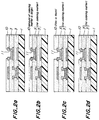
- Example 2 The same procedure as in Example 1 is repeated except that the varnish containing no coloring matter is used, whereby a multi-layer printed circuit board having a three-layer structure is produced. Then, a liquid composition for a photosensitive solder resist is applied to the multi-layer printed circuit board in the usual manner and subjected to exposure and development to form a solder resist 10 containing 2.0 wt% of phthalocyanine green and having a thickness of 30 ⁇ m at positions other than a pad portion 11 (Fig. 2b). Comparative Example 2
- Example 2c The same procedure as in Example 1 is repeated except that the varnish containing no coloring matter is used, whereby a multi-layer printed circuit board having a three-layer structure is produced. Then, a liquid composition for a photosensitive solder resist is applied to the multi-layer printed circuit board in the usual manner and subjected to exposure and development to form a solder resist 10 containing 1.0 wt% of phthalocyanine green and having a thickness of 70 ⁇ m at positions other than a pad portion 11 (Fig. 2c).
- Example 2d The same procedure as in Example 1 is repeated except that the varnish containing no coloring matter is used, whereby a multi-layer printed circuit board having a three-layer structure is produced. Then, a liquid composition for a photosensitive solder resist is applied to the multi-layer printed circuit board in the usual manner and subjected to exposure and development to form a solder resist 10 containing 1.0 wt% of phthalocyanine green and having a thickness of 30 ⁇ m at positions other than a pad portion 11 (Fig. 2d).
- the invention satisfy all of the above conditions and can advantageously provide printed circuit boards having excellent appearance and color tone without damaging the reliability and the like.
- the printed circuit boards of Example 1 and Comparative Example 3 are stored in an atmosphere having a humidity of 85%, an oxygen concentration of 100% and a temperature of 85°C, which is exposed to an ultraviolet ray at 1 J/cm2 ⁇ min to conduct deterioration test.
- the coloring matter such as phthalocyanine can control the deterioration of the photosensitive resin.
Landscapes
- Engineering & Computer Science (AREA)
- Microelectronics & Electronic Packaging (AREA)
- Manufacturing & Machinery (AREA)
- Architecture (AREA)
- Structural Engineering (AREA)
- Physics & Mathematics (AREA)
- General Physics & Mathematics (AREA)
- Compositions Of Macromolecular Compounds (AREA)
- Production Of Multi-Layered Print Wiring Board (AREA)
- Manufacturing Of Printed Wiring (AREA)
Applications Claiming Priority (2)
| Application Number | Priority Date | Filing Date | Title |
|---|---|---|---|
| JP10996193 | 1993-04-12 | ||
| JP109961/93 | 1993-04-12 |
Publications (2)
| Publication Number | Publication Date |
|---|---|
| EP0620703A1 true EP0620703A1 (de) | 1994-10-19 |
| EP0620703B1 EP0620703B1 (de) | 1997-12-29 |
Family
ID=14523536
Family Applications (1)
| Application Number | Title | Priority Date | Filing Date |
|---|---|---|---|
| EP94105576A Expired - Lifetime EP0620703B1 (de) | 1993-04-12 | 1994-04-11 | Harzzusammensetzungen und diese verwendende Leiterplatten |
Country Status (3)
| Country | Link |
|---|---|
| US (1) | US5589250A (de) |
| EP (1) | EP0620703B1 (de) |
| DE (1) | DE69407467T2 (de) |
Cited By (3)
| Publication number | Priority date | Publication date | Assignee | Title |
|---|---|---|---|---|
| CN1092918C (zh) * | 1995-04-28 | 2002-10-16 | 日本胜利株式会社 | 多层印刷电路板及其制造方法 |
| EP0952762A4 (de) * | 1996-12-19 | 2005-08-31 | Ibiden Co Ltd | Leiterplatte und verfahren zur herstellung |
| EP1699278A3 (de) * | 1998-09-28 | 2007-04-18 | Ibiden Co., Ltd. | Mehrlagen Schaltungsplatte und Verfahren zur Herstellung |
Families Citing this family (23)
| Publication number | Priority date | Publication date | Assignee | Title |
|---|---|---|---|---|
| US6205657B1 (en) | 1996-11-08 | 2001-03-27 | Matsushita Electric Industrial Co., Ltd. | Printed circuit board and method for producing the same |
| US6105243A (en) * | 1996-12-05 | 2000-08-22 | International Business Machines, Corp. | Method of fabricating multilayer printed circuit board |
| US6027709A (en) * | 1997-01-10 | 2000-02-22 | Li-Cor Inc. | Fluorescent cyanine dyes |
| JP3346263B2 (ja) * | 1997-04-11 | 2002-11-18 | イビデン株式会社 | プリント配線板及びその製造方法 |
| US6141870A (en) | 1997-08-04 | 2000-11-07 | Peter K. Trzyna | Method for making electrical device |
| WO1999034654A1 (en) * | 1997-12-29 | 1999-07-08 | Ibiden Co., Ltd. | Multilayer printed wiring board |
| MY120077A (en) * | 1998-06-26 | 2005-08-30 | Ibiden Co Ltd | Multilayer printed wiring board having a roughened inner conductor layer and production method thereof |
| JP2000294922A (ja) | 1999-04-01 | 2000-10-20 | Victor Co Of Japan Ltd | 多層プリント配線板用の絶縁樹脂組成物 |
| JP2000294921A (ja) * | 1999-04-01 | 2000-10-20 | Victor Co Of Japan Ltd | プリンス基板及びその製造方法 |
| KR100717909B1 (ko) * | 2006-02-24 | 2007-05-14 | 삼성전기주식회사 | 니켈층을 포함하는 기판 및 이의 제조방법 |
| US8344158B2 (en) * | 2007-08-15 | 2013-01-01 | Washington University | Fluorescent polymethine cyanine dyes |
| US20090214436A1 (en) | 2008-02-18 | 2009-08-27 | Washington University | Dichromic fluorescent compounds |
| JPWO2010087336A1 (ja) * | 2009-01-27 | 2012-08-02 | パナソニック株式会社 | 半導体チップの実装方法、該方法を用いて得られた半導体装置及び半導体チップの接続方法、並びに、表面に配線が設けられた立体構造物及びその製法 |
| EP3553075B1 (de) | 2012-01-23 | 2025-01-08 | Washington University | Brillenbildgebungssysteme und -verfahren |
| US20130284500A1 (en) * | 2012-04-25 | 2013-10-31 | Jun-Chung Hsu | Laminate circuit board structure |
| JP6057641B2 (ja) * | 2012-09-20 | 2017-01-11 | 新光電気工業株式会社 | 配線基板及びその製造方法 |
| KR101432446B1 (ko) * | 2013-06-13 | 2014-08-20 | 삼성전기주식회사 | 포토레지스트 현상용 조성물 및 이를 이용한 포토레지스트의 현상방법 |
| US10806804B2 (en) | 2015-05-06 | 2020-10-20 | Washington University | Compounds having RD targeting motifs and methods of use thereof |
| CN107851501B (zh) * | 2015-08-05 | 2020-01-07 | 株式会社村田制作所 | 电感元件及其制造方法 |
| CN108751125A (zh) * | 2018-06-07 | 2018-11-06 | 皖西学院 | 一种提高光刻胶胶层与电铸金属层界面结合力的方法 |
| CN112334267B (zh) * | 2019-01-28 | 2022-04-26 | 富士电机株式会社 | 钎焊接合部 |
| WO2021119423A1 (en) | 2019-12-13 | 2021-06-17 | Washington University | Near infrared fluorescent dyes, formulations and related methods |
| JP7518395B2 (ja) * | 2021-12-20 | 2024-07-18 | 日亜化学工業株式会社 | 回路基板、発光装置及びそれらの製造方法 |
Citations (5)
| Publication number | Priority date | Publication date | Assignee | Title |
|---|---|---|---|---|
| JPS5432769A (en) * | 1977-08-17 | 1979-03-10 | Hitachi Chemical Co Ltd | Method of making print wire board |
| US4752499A (en) * | 1985-05-16 | 1988-06-21 | Ibiden Co. Ltd. | Adhesive for electroless plating and method of preparation of circuit board using this adhesive |
| JPS648476B2 (de) * | 1979-10-31 | 1989-02-14 | Kureha Chemical Ind Co Ltd | |
| DE3913966A1 (de) * | 1988-04-28 | 1989-11-09 | Ibiden Co Ltd | Klebstoff zum stromlosen plattieren und gedruckte schaltung unter verwendung dieses klebstoffs |
| JPH04164392A (ja) * | 1990-10-29 | 1992-06-10 | Matsushita Electric Ind Co Ltd | 多層プリント配線板 |
Family Cites Families (6)
| Publication number | Priority date | Publication date | Assignee | Title |
|---|---|---|---|---|
| US3873309A (en) * | 1970-06-18 | 1975-03-25 | Xerox Corp | Imaging method using migration material |
| US3962520A (en) * | 1973-06-20 | 1976-06-08 | Sumitomo Bakelite Company, Limited | Adhesive composition for flexible printed circuit and method for using the same |
| US5135717A (en) * | 1986-12-24 | 1992-08-04 | British Technology Group Usa Inc. | Tetrabenztriazaporphyrin reagents and kits containing the same |
| JPH0455555A (ja) * | 1990-06-25 | 1992-02-24 | Misawa Homes Co Ltd | 建物の手摺支柱の設置構造 |
| JPH0518476A (ja) * | 1991-07-09 | 1993-01-26 | Sanmei Denki Kk | 電磁弁用端子箱 |
| US5344893A (en) * | 1991-07-23 | 1994-09-06 | Ibiden Co., Ltd. | Epoxy/amino powder resin adhesive for printed circuit board |
-
1994
- 1994-04-11 DE DE69407467T patent/DE69407467T2/de not_active Expired - Lifetime
- 1994-04-11 EP EP94105576A patent/EP0620703B1/de not_active Expired - Lifetime
-
1995
- 1995-08-23 US US08/518,358 patent/US5589250A/en not_active Expired - Lifetime
Patent Citations (5)
| Publication number | Priority date | Publication date | Assignee | Title |
|---|---|---|---|---|
| JPS5432769A (en) * | 1977-08-17 | 1979-03-10 | Hitachi Chemical Co Ltd | Method of making print wire board |
| JPS648476B2 (de) * | 1979-10-31 | 1989-02-14 | Kureha Chemical Ind Co Ltd | |
| US4752499A (en) * | 1985-05-16 | 1988-06-21 | Ibiden Co. Ltd. | Adhesive for electroless plating and method of preparation of circuit board using this adhesive |
| DE3913966A1 (de) * | 1988-04-28 | 1989-11-09 | Ibiden Co Ltd | Klebstoff zum stromlosen plattieren und gedruckte schaltung unter verwendung dieses klebstoffs |
| JPH04164392A (ja) * | 1990-10-29 | 1992-06-10 | Matsushita Electric Ind Co Ltd | 多層プリント配線板 |
Non-Patent Citations (2)
| Title |
|---|
| DATABASE WPI Week 7916, Derwent World Patents Index; AN 79-30724B * |
| PATENT ABSTRACTS OF JAPAN vol. 16, no. 465 (E - 1270) 28 September 1992 (1992-09-28) * |
Cited By (26)
| Publication number | Priority date | Publication date | Assignee | Title |
|---|---|---|---|---|
| CN1092918C (zh) * | 1995-04-28 | 2002-10-16 | 日本胜利株式会社 | 多层印刷电路板及其制造方法 |
| CN100435605C (zh) * | 1996-12-19 | 2008-11-19 | 揖斐电株式会社 | 印刷布线板 |
| US7585541B2 (en) | 1996-12-19 | 2009-09-08 | Ibiden Co., Ltd. | Printed wiring board and method for manufacturing the same |
| USRE43509E1 (en) | 1996-12-19 | 2012-07-17 | Ibiden Co., Ltd. | Printed wiring board and method for manufacturing the same |
| EP1921902A3 (de) * | 1996-12-19 | 2009-03-25 | Ibiden Co., Ltd. | Leiterplatte und Herstellungsverfahren dafür |
| US7361849B2 (en) | 1996-12-19 | 2008-04-22 | Ibiden Co., Ltd. | Printed wiring board and method for manufacturing the same |
| US7371976B2 (en) | 1996-12-19 | 2008-05-13 | Ibiden Co., Ltd. | Printed wiring board and method for manufacturing the same |
| US7385146B2 (en) | 1996-12-19 | 2008-06-10 | Ibiden Co., Ltd. | Printed wiring board and method for manufacturing the same |
| US7388159B2 (en) | 1996-12-19 | 2008-06-17 | Ibiden Co., Ltd. | Printed wiring board and method for manufacturing the same |
| US7712212B2 (en) | 1996-12-19 | 2010-05-11 | Ibiden Co., Ltd. | Method for manufacturing printed wiring board |
| US7615162B2 (en) | 1996-12-19 | 2009-11-10 | Ibiden Co., Ltd. | Printed wiring board and method for manufacturing the same |
| US7449791B2 (en) | 1996-12-19 | 2008-11-11 | Ibiden Co., Ltd. | Printed circuit boards and method of producing the same |
| EP0952762A4 (de) * | 1996-12-19 | 2005-08-31 | Ibiden Co Ltd | Leiterplatte und verfahren zur herstellung |
| US8030577B2 (en) | 1998-09-28 | 2011-10-04 | Ibiden Co., Ltd. | Printed wiring board and method for producing the same |
| US7535095B1 (en) | 1998-09-28 | 2009-05-19 | Ibiden Co., Ltd. | Printed wiring board and method for producing the same |
| US7504719B2 (en) | 1998-09-28 | 2009-03-17 | Ibiden Co., Ltd. | Printed wiring board having a roughened surface formed on a metal layer, and method for producing the same |
| EP1699278A3 (de) * | 1998-09-28 | 2007-04-18 | Ibiden Co., Ltd. | Mehrlagen Schaltungsplatte und Verfahren zur Herstellung |
| EP1978797A3 (de) * | 1998-09-28 | 2008-10-22 | Ibiden Co., Ltd. | Mehrschichtige Leiterplatte und Herstellungsverfahren dafür |
| EP1978796A3 (de) * | 1998-09-28 | 2008-10-22 | Ibiden Co., Ltd. | Leiterplatte und Herstellungsverfahren dafür |
| US7994433B2 (en) | 1998-09-28 | 2011-08-09 | Ibiden Co., Ltd. | Printed wiring board and method for producing the same |
| US8018045B2 (en) | 1998-09-28 | 2011-09-13 | Ibiden Co., Ltd. | Printed circuit board |
| US8020291B2 (en) | 1998-09-28 | 2011-09-20 | Ibiden Co., Ltd. | Method of manufacturing a printed wiring board |
| EP1830617A3 (de) * | 1998-09-28 | 2007-12-19 | Ibiden Co., Ltd. | Mehrschichtleiterplatte und Herstellungsverfahren dafür |
| US8093507B2 (en) | 1998-09-28 | 2012-01-10 | Ibiden Co., Ltd. | Printed wiring board and method for producing the same |
| EP1830617A2 (de) | 1998-09-28 | 2007-09-05 | Ibiden Co., Ltd. | Mehrschichtleiterplatte und Herstellungsverfahren dafür |
| US8533943B2 (en) | 1998-09-28 | 2013-09-17 | Ibiden Co., Ltd. | Printed wiring board and method for producing the same |
Also Published As
| Publication number | Publication date |
|---|---|
| DE69407467T2 (de) | 1998-04-16 |
| EP0620703B1 (de) | 1997-12-29 |
| US5589250A (en) | 1996-12-31 |
| DE69407467D1 (de) | 1998-02-05 |
Similar Documents
| Publication | Publication Date | Title |
|---|---|---|
| EP0620703B1 (de) | Harzzusammensetzungen und diese verwendende Leiterplatten | |
| KR100330277B1 (ko) | 솔더레지스트 조성물 및 프린트배선판 | |
| DE69938182T2 (de) | Mehrschichtige leiterplatte und verfahren zu deren herstellung | |
| US6376049B1 (en) | Multilayer printed wiring board and its manufacturing method, and resin composition for filling through-hole | |
| US5589255A (en) | Adhesive for electroless plating, printed circuit boards and method of producing the same | |
| DE112005002748B4 (de) | Mit Adhäsionshilfsmittel ausgestattete Metallfolie,Leiterplatte, bei der diese verwendet wird, und Verfahren zurHerstellung einer Leiterplatte | |
| WO1999003316A1 (en) | Printed wiring board and method for manufacturing the same | |
| US4305975A (en) | Method of forming printed circuit | |
| KR20010006375A (ko) | 무전해 도금용 접착제, 무전해 도금용 접착제 조제용의 원료조성물 및 프린트 배선판 | |
| JPH06275959A (ja) | 多層配線基板とその製造方法および両面プリント配線板の製造方法 | |
| CN101478861B (zh) | 多层印刷电路板 | |
| KR100417544B1 (ko) | 인쇄 회로 보드, 인쇄 회로 보드 제조 방법, 및 유전 중합체 합성물 | |
| JP3311977B2 (ja) | 無電解めっき用接着剤および多層プリント配線板 | |
| JPH06260756A (ja) | プリント配線板の製造方法 | |
| JPH11126974A (ja) | 多層配線板の製造方法 | |
| JPH06260763A (ja) | 多層配線基板の製造方法 | |
| JP3142423B2 (ja) | プリント配線板 | |
| JP3297006B2 (ja) | 多層プリント配線板 | |
| JP3300653B2 (ja) | 無電解めっき用接着剤および多層プリント配線板 | |
| JP2000077851A (ja) | 多層プリント配線板の製造方法 | |
| JP3469214B2 (ja) | ビルドアップ多層プリント配線板 | |
| JP3469146B2 (ja) | ビルドアップ多層プリント配線板 | |
| JP4126735B2 (ja) | 特定の酸化防止剤を含む絶縁樹脂を用いた多層配線板の製造方法 | |
| JPH077266A (ja) | 多層プリント配線板の製造方法 | |
| JP2000124607A (ja) | 多層プリント配線板及びその製造方法 |
Legal Events
| Date | Code | Title | Description |
|---|---|---|---|
| PUAI | Public reference made under article 153(3) epc to a published international application that has entered the european phase |
Free format text: ORIGINAL CODE: 0009012 |
|
| AK | Designated contracting states |
Kind code of ref document: A1 Designated state(s): DE GB NL |
|
| 17P | Request for examination filed |
Effective date: 19950413 |
|
| 17Q | First examination report despatched |
Effective date: 19960123 |
|
| GRAG | Despatch of communication of intention to grant |
Free format text: ORIGINAL CODE: EPIDOS AGRA |
|
| GRAG | Despatch of communication of intention to grant |
Free format text: ORIGINAL CODE: EPIDOS AGRA |
|
| GRAH | Despatch of communication of intention to grant a patent |
Free format text: ORIGINAL CODE: EPIDOS IGRA |
|
| GRAH | Despatch of communication of intention to grant a patent |
Free format text: ORIGINAL CODE: EPIDOS IGRA |
|
| GRAA | (expected) grant |
Free format text: ORIGINAL CODE: 0009210 |
|
| AK | Designated contracting states |
Kind code of ref document: B1 Designated state(s): DE GB NL |
|
| REF | Corresponds to: |
Ref document number: 69407467 Country of ref document: DE Date of ref document: 19980205 |
|
| PLBE | No opposition filed within time limit |
Free format text: ORIGINAL CODE: 0009261 |
|
| STAA | Information on the status of an ep patent application or granted ep patent |
Free format text: STATUS: NO OPPOSITION FILED WITHIN TIME LIMIT |
|
| 26N | No opposition filed | ||
| REG | Reference to a national code |
Ref country code: GB Ref legal event code: IF02 |
|
| PGFP | Annual fee paid to national office [announced via postgrant information from national office to epo] |
Ref country code: NL Payment date: 20120425 Year of fee payment: 19 Ref country code: DE Payment date: 20120425 Year of fee payment: 19 |
|
| PGFP | Annual fee paid to national office [announced via postgrant information from national office to epo] |
Ref country code: GB Payment date: 20120411 Year of fee payment: 19 |
|
| REG | Reference to a national code |
Ref country code: NL Ref legal event code: V1 Effective date: 20131101 |
|
| GBPC | Gb: european patent ceased through non-payment of renewal fee |
Effective date: 20130411 |
|
| PG25 | Lapsed in a contracting state [announced via postgrant information from national office to epo] |
Ref country code: DE Free format text: LAPSE BECAUSE OF NON-PAYMENT OF DUE FEES Effective date: 20131101 Ref country code: GB Free format text: LAPSE BECAUSE OF NON-PAYMENT OF DUE FEES Effective date: 20130411 |
|
| REG | Reference to a national code |
Ref country code: DE Ref legal event code: R119 Ref document number: 69407467 Country of ref document: DE Effective date: 20131101 |
|
| PG25 | Lapsed in a contracting state [announced via postgrant information from national office to epo] |
Ref country code: NL Free format text: LAPSE BECAUSE OF NON-PAYMENT OF DUE FEES Effective date: 20131101 |