EP0621729A1 - Dispositif de visualisation sur écran d'une première image dans une seconde image - Google Patents
Dispositif de visualisation sur écran d'une première image dans une seconde image Download PDFInfo
- Publication number
- EP0621729A1 EP0621729A1 EP94104892A EP94104892A EP0621729A1 EP 0621729 A1 EP0621729 A1 EP 0621729A1 EP 94104892 A EP94104892 A EP 94104892A EP 94104892 A EP94104892 A EP 94104892A EP 0621729 A1 EP0621729 A1 EP 0621729A1
- Authority
- EP
- European Patent Office
- Prior art keywords
- image
- signals
- signal
- digital
- output current
- Prior art date
- Legal status (The legal status is an assumption and is not a legal conclusion. Google has not performed a legal analysis and makes no representation as to the accuracy of the status listed.)
- Granted
Links
- 238000006243 chemical reaction Methods 0.000 claims description 25
- 238000001514 detection method Methods 0.000 claims 1
- 238000010586 diagram Methods 0.000 description 5
- 238000004519 manufacturing process Methods 0.000 description 3
- 239000004065 semiconductor Substances 0.000 description 3
- 238000012432 intermediate storage Methods 0.000 description 2
- 208000032041 Hearing impaired Diseases 0.000 description 1
- 230000001419 dependent effect Effects 0.000 description 1
- 238000011161 development Methods 0.000 description 1
- 230000018109 developmental process Effects 0.000 description 1
- 238000010894 electron beam technology Methods 0.000 description 1
- 230000009191 jumping Effects 0.000 description 1
Images


Classifications
-
- H—ELECTRICITY
- H04—ELECTRIC COMMUNICATION TECHNIQUE
- H04N—PICTORIAL COMMUNICATION, e.g. TELEVISION
- H04N5/00—Details of television systems
- H04N5/44—Receiver circuitry for the reception of television signals according to analogue transmission standards
- H04N5/445—Receiver circuitry for the reception of television signals according to analogue transmission standards for displaying additional information
- H04N5/45—Picture in picture, e.g. displaying simultaneously another television channel in a region of the screen
-
- H—ELECTRICITY
- H04—ELECTRIC COMMUNICATION TECHNIQUE
- H04N—PICTORIAL COMMUNICATION, e.g. TELEVISION
- H04N5/00—Details of television systems
- H04N5/44—Receiver circuitry for the reception of television signals according to analogue transmission standards
- H04N5/57—Control of contrast or brightness
Definitions
- the invention relates to a device for displaying a first image and a second image on a screen according to the preamble of claim 1.
- Such a device is known for example from Siemens Components, Issue 1, 1990.
- this arrangement has a picture-in-picture processor (SDA 9088) from Siemens, which enables a reduced picture to be superimposed on a larger main picture.
- SDA 9088 picture-in-picture processor
- Both image sources can be chosen completely independently with regard to the television standard and synchronization.
- the picture-in-picture processor takes over the image reduction, the intermediate storage of this reduced image in an integrated image memory and the output of the image data of this reduced image via a digital-to-analog conversion stage, so that the image signal for the reduced image at the output of the image in the image processor in analog form.
- the second image processing stage which provides image signals for the second image from a second video signal source, can in principle have an analog or digital structure.
- the structure and mode of operation of such a second image signal processing stage in digital form is described for example in Siemens Components, Issue 6, 1988 on pages 240 to 245.
- analog image signals can be tapped at the output of this second image processing stage.
- a switching device on Output of the first and second image processing stage ensures a timely switching between the image signals for the reduced first image and the second main image, so that a small image shown in a large image becomes visible on the screen of the television set.
- Another possibility for adjusting the contrast would be to provide an amplitude control for both the first and the second image signal in the switching device.
- this would inevitably lead to a switching device which is complex in terms of its circuitry structure and which is therefore expensive.
- This device has a first image processing stage for generating first image signals and a second image processing stage for generating second image signals and a switching device for switching between these first and second image signals.
- at least one variable reference signal can be fed to a D / A stage connected on the output side to the first image processing stage, which can be set by a control device in accordance with digital control signals.
- the invention is therefore based on the object of developing this known device in such a way that such tolerances when adjusting the contrast of an image to be faded in do not lead to an unwanted change in contrast of the image to be faded in.
- image sources of the most varied types can be used for the first and second images, for example television programs, video cameras or video recorders.
- subtitles e.g. B. for hearing impaired in a main picture, as is currently possible in connection with the teletext or teletext signals broadcast by the television stations.
- the contrast of the first image can be adapted to the contrast of the second image or can be adjusted individually. Contrast deviations that occur due to manufacturing tolerances in the chip production of the D / A stage can be effectively compensated for. Such compensation can be carried out, for example, during an arbitrarily selectable time window. This window can be placed in an area in which no image is displayed on the screen. B. in the line return or image return of the electron beam.
- the device In order to be able to receive such teletext signals, the device must be suitable for receiving information in the form of coded characters which can be converted into image signals via a character generator.
- Integrated circuits for receiving such teletext signals are known, for example, from Siemens as SDA 5243 or SDA 5273.
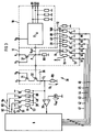
- first image processing stage 1 shows the basic circuit diagram for picture-in-picture overlay with a first image processing stage 1 and a second image processing stage 2.
- the first image processing stage 1 has input terminals 3, 4 for applying first video signals Video 1 and associated sync signals Sync 1.
- the second image processing stage 2 is provided with input terminals 5, 6 for second video signals video 2 and second synchronization signals sync 2.
- First analog image signals R1, G1, B1 can be tapped at output terminals of first image processing stage 1 and second analog image signals R2, G2, B2 at output terminals of second image processing stage 2.
- the first and second image signals R1, G1, B1; R2, G2, B2 arrive at a switching device 7, which switches between the first image signals R1, G1, B1 and second image signals R2, G2, B2 at the correct time.
- a control device 8 is connected via multicore connecting lines a, b, c to the first image processing stage 1, second image processing stage 2 and switching device 7 and provides suitable control signals for the correct control of the individual components.
- the first image processing stage 1 has a picture-in-picture processor, e.g. B. the integrated circuit SDA 9088 from Siemens, which is used via a signal processing stage 9, the image reduction, the intermediate storage of the digital image data in an integrated image memory and the output of the digital image data of the reduced image to digital-to-analog conversion stage 10.
- the digital-to-analog conversion stage 10 can be supplied with a variable reference signal Vref from a reference signal stage 11, this reference signal from the control device 8 Provided digital control signals b is adjustable.
- the digital-to-analog conversion stage 10 is a D / A converter with switchable current sources, as is described as such from Tietze-Schenk, Semiconductor Circuit Technology, 5th edition, 1980, under point 24.2.2.
- FIG. 2 shows the reference signal stage 11 and a device 30 according to the invention for detecting an amplitude deviation of output current signals IR1, IG1, IB1 of the digital-to-analog conversion stage 10 from a predetermined reference amplitude and for readjusting the output current signals IR1, IG1, IB1 of the digital-to-analog conversion stage 10 shown on the predetermined reference amplitude.
- a reference voltage Vref which is fed to the digital-to-analog conversion stage 10, serves as the reference signal.
- This reference voltage Vref is tapped at the output of a reference voltage generator device 40.
- the reference voltage stage 40 lies, for example, between a positive pole V +, a supply voltage source and a reference voltage V-.
- the reference voltage stage 40 can be connected in series to a resistor R8, in such a way that the reference voltage stage 40 and the resistor R8 are connected between the terminals V +, V-.
- the resistor R8 has one connection to the reference voltage V- and the other connection to the reference voltage stage 40.
- the connection point between the reference voltage stage 40 and the resistor R8 is denoted by P in FIG.
- the device 30 has a comparator 35 which is connected on the output side to the control device 8 and at which one input terminal, ie in this exemplary embodiment the inverting input terminal -, a predetermined reference signal Uref can be connected and to the latter another input terminal, ie in this case the non-inverting connection of the comparator 35, a signal can be applied which represents a measure of the output current signal IR1, IG1, IB1 of the digital-to-analog conversion stage 10.
- FIG. 3 it is explained in detail how, for example, the signal to be connected to the input terminal + of the comparator 35 can be obtained.
- the output terminal of the comparator 35 is connected to the control device 8, which, depending on the deviation between the signals at the input terminals -, + of the comparator 35, generates control signals in order to vary or readjust the above-mentioned voltage signal Vref of the reference voltage stage 40 that the output current signals IR1, IG1, IB1 of the digital-to-analog conversion stage 10 are set to a predetermined reference amplitude.
- a switchable voltage divider arrangement is provided in the illustration in FIG. 2, which is connected to the connection point P.
- the number of switchable resistors essentially determines the control accuracy and can be different from the number of 4 shown here. Specifically, the illustration in FIG.
- connection point P is additionally at an output terminal 12 of the first image processing stage. At this output terminal 12, a resistor connected to reference potential V- can be connected externally, as a result of which the reference voltage Vref is initially roughly defined.
- the control device 8 can switch the resistors 15 on and off. This changes the reference current of the current mirror shown in FIG. 2, which generates the reference voltage Vref for the digital-to-analog conversion stage 10.
- FIG. 3 shows a detailed circuit diagram of FIG. 2 of a device according to the invention.
- FIG. 2 shows a detailed circuit diagram of FIG. 2 of a device according to the invention.
- the reference voltage Vref which is supplied to the digital-analog conversion stage 10, is now tapped at the connection point P of a voltage divider which is connected between the positive pole V + of the supply voltage source and the reference voltage V-, here ground.
- the voltage divider consists of a MOS transistor 37 connected to the positive pole V + of the supply voltage source, the control connection of which is connected to a voltage VS, with a resistor R8 connected in series.
- the connection point P is also again at the output terminal 12 of the first image processing stage 1. At this output terminal 12, the reference voltage Vref can initially be roughly determined via a resistor to be connected.
- a total of six resistors 15 which can be connected in parallel are now connected to the connection point P, and their respective other connections are each connected to reference potential V- via a semiconductor switch 13, the control connections of the semiconductor switches 13 having terminals b1, b2, b3, b4, b5 and b6 are connected to which control signals 41, 42, 43, 44, 45 and 46 of control device 8 can be applied.
- These resistors can be switched on and off by means of these control signals b1 to b6. Switching these resistors 15 on and off directly influences the reference voltage Vref of the voltage divider shown in FIG.
- the resistors 15 have the values 2 / R, R, 2R, 4R, 8R and 16R.
- the reference voltage Vref for the digital-to-analog conversion stage 10 can be changed, which results in a change in the output current of the digital-to-analog conversion stage 10 without the properties thereof changing significantly.
- FIG. 3 shows a current source circuit 36 which contains a current source which is identical to the current sources of the digital-to-analog conversion stage 10. This current source circuit 36 is supplied with the variable voltage signal Vref as a control signal for generating an output current Is.
- the current source circuit 36 consists of the 3 of two MOS transistors 31, 32 connected in series, the first output terminal of the MOS transistor being connected to the positive pole V + of the supply voltage source and the second output terminal of this MOS transistor 31 being connected to a first output terminal of the MOS transistor 32.
- a second output terminal of this MOS transistor 32 is connected to reference voltage V- via a resistor R9.
- a control terminal of the MOS transistor 31 is connected to a terminal for a voltage VB and a control terminal of the MOS transistor 32 is connected to the connection point P.
- the reference voltage Vref is therefore also present at the control connection of the MOS transistor 32. Depending on the amplitude of this reference voltage Vref, a current IS is generated in the current source circuit 36.
- This current IS generates a voltage drop across the resistor R9, which is present as a signal at the non-inverting input terminal + of the comparator 35.
- the voltage Ur represents a measure of the output current signal IR1, IG1, IB1 of the digital-to-analog conversion stage 10 because of the identical current source design.
- the output of the comparator 35 is connected to the control device 8 in the manner already described in connection with FIG drives until the reference voltage Vref is as large as the voltage Uref.
- a digital counter can be provided in the control device 8, for example, which switches the MOS transistors 13 on or off via the control lines 41 to 46, until the voltage Ur across the resistor R9 is equal to the voltage Uref.
- a comparison can, for example, be carried out automatically with a delay after the device according to the invention has been switched on and can be started at any time by a suitable control command.
- the control device 8 connects resistors 53 in parallel to the resistor R9.
- the device has four resistors 53 which can be connected in parallel and which have one connection to the non-inverting input terminal + of the comparator 35 and the other connections are each connected via a MOS transistor 55 to reference potential V- are.
- the control connections of these MOS transistors 55 are connected to the control device 8 via control lines 61, 62, 63, 64.
- An advantage of the device according to the invention in comparison with a previously conventional manual control is that the adjustment can only be carried out during an arbitrarily selectable time window.
- This window can be in a time range in which no image is displayed on the screen. This reduces disturbances to the control to a minimum.
Landscapes
- Engineering & Computer Science (AREA)
- Multimedia (AREA)
- Signal Processing (AREA)
- Television Receiver Circuits (AREA)
Applications Claiming Priority (2)
| Application Number | Priority Date | Filing Date | Title |
|---|---|---|---|
| DE4313228 | 1993-04-22 | ||
| DE4313228 | 1993-04-22 |
Publications (2)
| Publication Number | Publication Date |
|---|---|
| EP0621729A1 true EP0621729A1 (fr) | 1994-10-26 |
| EP0621729B1 EP0621729B1 (fr) | 1998-02-25 |
Family
ID=6486131
Family Applications (1)
| Application Number | Title | Priority Date | Filing Date |
|---|---|---|---|
| EP94104892A Expired - Lifetime EP0621729B1 (fr) | 1993-04-22 | 1994-03-28 | Dispositif de visualisation sur écran d'une première image dans une seconde image |
Country Status (3)
| Country | Link |
|---|---|
| EP (1) | EP0621729B1 (fr) |
| DE (1) | DE59405283D1 (fr) |
| ES (1) | ES2113006T3 (fr) |
Cited By (3)
| Publication number | Priority date | Publication date | Assignee | Title |
|---|---|---|---|---|
| EP0675644A3 (fr) * | 1994-03-23 | 1995-11-15 | Toshiba Kk | |
| EP0713334A3 (fr) * | 1994-11-17 | 1997-12-17 | Matsushita Electric Industrial Co., Ltd. | Procédé et appareil d'enregistrement/de reproduction d'image en temps réel, et système de bibliothèque vidéo |
| EP1096794A3 (fr) * | 1999-10-26 | 2004-10-20 | Thomson Licensing S.A. | Dispositif d'ajustage d'une image multi-fenêtres pour un dispositif d'affichage vidéo |
Citations (5)
| Publication number | Priority date | Publication date | Assignee | Title |
|---|---|---|---|---|
| JPS60257682A (ja) * | 1984-06-04 | 1985-12-19 | Matsushita Electric Ind Co Ltd | 映像制御装置 |
| JPS6180977A (ja) * | 1984-09-28 | 1986-04-24 | Toshiba Corp | テレビジヨン受像機 |
| US4721943A (en) * | 1985-10-11 | 1988-01-26 | Tektronix, Inc. | Digital-to-analog converter for video application |
| EP0281116A2 (fr) * | 1987-03-04 | 1988-09-07 | Kabushiki Kaisha Toshiba | Convertisseur numérique-analogique |
| EP0443064A1 (fr) * | 1990-02-19 | 1991-08-28 | Siemens Aktiengesellschaft | Dispositif d'insertion d'une première image dans une deuxième image sur un écran |
-
1994
- 1994-03-28 ES ES94104892T patent/ES2113006T3/es not_active Expired - Lifetime
- 1994-03-28 DE DE59405283T patent/DE59405283D1/de not_active Expired - Fee Related
- 1994-03-28 EP EP94104892A patent/EP0621729B1/fr not_active Expired - Lifetime
Patent Citations (5)
| Publication number | Priority date | Publication date | Assignee | Title |
|---|---|---|---|---|
| JPS60257682A (ja) * | 1984-06-04 | 1985-12-19 | Matsushita Electric Ind Co Ltd | 映像制御装置 |
| JPS6180977A (ja) * | 1984-09-28 | 1986-04-24 | Toshiba Corp | テレビジヨン受像機 |
| US4721943A (en) * | 1985-10-11 | 1988-01-26 | Tektronix, Inc. | Digital-to-analog converter for video application |
| EP0281116A2 (fr) * | 1987-03-04 | 1988-09-07 | Kabushiki Kaisha Toshiba | Convertisseur numérique-analogique |
| EP0443064A1 (fr) * | 1990-02-19 | 1991-08-28 | Siemens Aktiengesellschaft | Dispositif d'insertion d'une première image dans une deuxième image sur un écran |
Non-Patent Citations (2)
| Title |
|---|
| PATENT ABSTRACTS OF JAPAN vol. 10, no. 125 (E - 402) 10 May 1986 (1986-05-10) * |
| PATENT ABSTRACTS OF JAPAN vol. 10, no. 251 (E - 432) 28 August 1986 (1986-08-28) * |
Cited By (5)
| Publication number | Priority date | Publication date | Assignee | Title |
|---|---|---|---|---|
| EP0675644A3 (fr) * | 1994-03-23 | 1995-11-15 | Toshiba Kk | |
| US5675391A (en) * | 1994-03-23 | 1997-10-07 | Kabushiki Kaisha Toshiba | Contrast/brightness control circuit for television receiver |
| EP0713334A3 (fr) * | 1994-11-17 | 1997-12-17 | Matsushita Electric Industrial Co., Ltd. | Procédé et appareil d'enregistrement/de reproduction d'image en temps réel, et système de bibliothèque vidéo |
| US5822493A (en) * | 1994-11-17 | 1998-10-13 | Matsushita Electric Industrial Co., Ltd. | Real-time image recording/producing method and apparatus and video library system |
| EP1096794A3 (fr) * | 1999-10-26 | 2004-10-20 | Thomson Licensing S.A. | Dispositif d'ajustage d'une image multi-fenêtres pour un dispositif d'affichage vidéo |
Also Published As
| Publication number | Publication date |
|---|---|
| EP0621729B1 (fr) | 1998-02-25 |
| DE59405283D1 (de) | 1998-04-02 |
| ES2113006T3 (es) | 1998-04-16 |
Similar Documents
| Publication | Publication Date | Title |
|---|---|---|
| DE3782013T2 (de) | Analog-digital-umwandler mit automatischer verstaerkungsregelung. | |
| DE2252181C3 (de) | Videoverstärker für ein Farbfernsehbildüberwachungsgerät | |
| DE2516899C2 (de) | Signal-Klemmschaltung | |
| DE3838000C2 (de) | Videoproduktionseinrichtung | |
| EP0939494B1 (fr) | Montage de convertisseurs numériques-analogiques du type à courant | |
| DE3440705A1 (de) | Schaltungsanordnung zur wiedereinfuehrung der gleichstromkomponente in einem videosignal | |
| AT390859B (de) | Schaltungsanordnung zur automatischen regelung des schwarzstrompegels einer bildroehre | |
| DE1462893B2 (de) | Verfahren und vorrichtung zur steuerung der helligkeit und des kontrastes einer bildroehre | |
| DE2121333A1 (de) | Fernsehkamera mit elektronischer Bildausschnittsänderung durch Steuerung des Ablenksystems | |
| EP0443064B1 (fr) | Dispositif d'insertion d'une première image dans une deuxième image sur un écran | |
| DE3632484C2 (fr) | ||
| DE3024267C2 (de) | Schaltanordnung für Fernsehsignale | |
| EP0621729B1 (fr) | Dispositif de visualisation sur écran d'une première image dans une seconde image | |
| DE4203092A1 (de) | Verfahren zur kontrastkorrektur | |
| DD237563A5 (de) | Digitales bildsignalverarbeitungs- und wiedergabesystem | |
| DE4006416A1 (de) | Polygonschaltung | |
| DE3632864C2 (fr) | ||
| DE3337299C3 (fr) | ||
| DE3419645C2 (de) | Transversalfilter mit MOS-Transistor-Verstärkern | |
| EP0230924A2 (fr) | Arrangement de circuit pour la commande du point de fonctionnement dynamique des étages finals de vidéo à large bande | |
| DE2748532A1 (de) | Geregelter farbverstaerker | |
| AT392713B (de) | Schaltungsanordnung zur zufuhr von ablenksteuersignalen zu den horizontal- bzw. vertikalablenkeinrichtungen in einer mehrroehren-fernsehkamera | |
| EP0568982B2 (fr) | Méthode et dispositif de correction d'image numérique | |
| DE2325028A1 (de) | Schaltung zur speisung einer ablenkspule fuer eine kathodenstrahlroehre, insbesondere fuer die vertikalablenkung | |
| DE2804120B2 (de) | Schaltungsanordnung zum Einjustieren der Betriebsparameter einer Farbbildwiedergaberöhre |
Legal Events
| Date | Code | Title | Description |
|---|---|---|---|
| PUAI | Public reference made under article 153(3) epc to a published international application that has entered the european phase |
Free format text: ORIGINAL CODE: 0009012 |
|
| AK | Designated contracting states |
Kind code of ref document: A1 Designated state(s): DE ES FR GB IT |
|
| 17P | Request for examination filed |
Effective date: 19950321 |
|
| GRAG | Despatch of communication of intention to grant |
Free format text: ORIGINAL CODE: EPIDOS AGRA |
|
| GRAG | Despatch of communication of intention to grant |
Free format text: ORIGINAL CODE: EPIDOS AGRA |
|
| GRAH | Despatch of communication of intention to grant a patent |
Free format text: ORIGINAL CODE: EPIDOS IGRA |
|
| 17Q | First examination report despatched |
Effective date: 19970725 |
|
| GRAH | Despatch of communication of intention to grant a patent |
Free format text: ORIGINAL CODE: EPIDOS IGRA |
|
| GRAA | (expected) grant |
Free format text: ORIGINAL CODE: 0009210 |
|
| AK | Designated contracting states |
Kind code of ref document: B1 Designated state(s): DE ES FR GB IT |
|
| REF | Corresponds to: |
Ref document number: 59405283 Country of ref document: DE Date of ref document: 19980402 |
|
| REG | Reference to a national code |
Ref country code: ES Ref legal event code: FG2A Ref document number: 2113006 Country of ref document: ES Kind code of ref document: T3 |
|
| ET | Fr: translation filed | ||
| ITF | It: translation for a ep patent filed | ||
| GBT | Gb: translation of ep patent filed (gb section 77(6)(a)/1977) |
Effective date: 19980429 |
|
| PLBE | No opposition filed within time limit |
Free format text: ORIGINAL CODE: 0009261 |
|
| STAA | Information on the status of an ep patent application or granted ep patent |
Free format text: STATUS: NO OPPOSITION FILED WITHIN TIME LIMIT |
|
| 26N | No opposition filed | ||
| PGFP | Annual fee paid to national office [announced via postgrant information from national office to epo] |
Ref country code: DE Payment date: 20000523 Year of fee payment: 7 |
|
| REG | Reference to a national code |
Ref country code: GB Ref legal event code: 732E |
|
| PG25 | Lapsed in a contracting state [announced via postgrant information from national office to epo] |
Ref country code: DE Free format text: LAPSE BECAUSE OF NON-PAYMENT OF DUE FEES Effective date: 20020101 |
|
| REG | Reference to a national code |
Ref country code: GB Ref legal event code: IF02 |
|
| PGFP | Annual fee paid to national office [announced via postgrant information from national office to epo] |
Ref country code: ES Payment date: 20020409 Year of fee payment: 9 |
|
| PG25 | Lapsed in a contracting state [announced via postgrant information from national office to epo] |
Ref country code: ES Free format text: LAPSE BECAUSE OF NON-PAYMENT OF DUE FEES Effective date: 20030329 |
|
| REG | Reference to a national code |
Ref country code: ES Ref legal event code: FD2A Effective date: 20030329 |
|
| PGFP | Annual fee paid to national office [announced via postgrant information from national office to epo] |
Ref country code: GB Payment date: 20070327 Year of fee payment: 14 |
|
| PGFP | Annual fee paid to national office [announced via postgrant information from national office to epo] |
Ref country code: IT Payment date: 20070523 Year of fee payment: 14 |
|
| PGFP | Annual fee paid to national office [announced via postgrant information from national office to epo] |
Ref country code: FR Payment date: 20070319 Year of fee payment: 14 |
|
| GBPC | Gb: european patent ceased through non-payment of renewal fee |
Effective date: 20080328 |
|
| REG | Reference to a national code |
Ref country code: FR Ref legal event code: ST Effective date: 20081125 |
|
| PG25 | Lapsed in a contracting state [announced via postgrant information from national office to epo] |
Ref country code: FR Free format text: LAPSE BECAUSE OF NON-PAYMENT OF DUE FEES Effective date: 20080331 |
|
| PG25 | Lapsed in a contracting state [announced via postgrant information from national office to epo] |
Ref country code: GB Free format text: LAPSE BECAUSE OF NON-PAYMENT OF DUE FEES Effective date: 20080328 |
|
| PG25 | Lapsed in a contracting state [announced via postgrant information from national office to epo] |
Ref country code: IT Free format text: LAPSE BECAUSE OF NON-PAYMENT OF DUE FEES Effective date: 20080328 |