EP0568982B2 - Méthode et dispositif de correction d'image numérique - Google Patents
Méthode et dispositif de correction d'image numérique Download PDFInfo
- Publication number
- EP0568982B2 EP0568982B2 EP93107232A EP93107232A EP0568982B2 EP 0568982 B2 EP0568982 B2 EP 0568982B2 EP 93107232 A EP93107232 A EP 93107232A EP 93107232 A EP93107232 A EP 93107232A EP 0568982 B2 EP0568982 B2 EP 0568982B2
- Authority
- EP
- European Patent Office
- Prior art keywords
- signal
- signals
- regulating
- actuating
- correction
- Prior art date
- Legal status (The legal status is an assumption and is not a legal conclusion. Google has not performed a legal analysis and makes no representation as to the accuracy of the status listed.)
- Expired - Lifetime
Links
Images


Classifications
-
- H—ELECTRICITY
- H04—ELECTRIC COMMUNICATION TECHNIQUE
- H04N—PICTORIAL COMMUNICATION, e.g. TELEVISION
- H04N9/00—Details of colour television systems
- H04N9/12—Picture reproducers
- H04N9/16—Picture reproducers using cathode ray tubes
- H04N9/28—Arrangements for convergence or focusing
-
- H—ELECTRICITY
- H04—ELECTRIC COMMUNICATION TECHNIQUE
- H04N—PICTORIAL COMMUNICATION, e.g. TELEVISION
- H04N3/00—Scanning details of television systems; Combination thereof with generation of supply voltages
- H04N3/10—Scanning details of television systems; Combination thereof with generation of supply voltages by means not exclusively optical-mechanical
- H04N3/16—Scanning details of television systems; Combination thereof with generation of supply voltages by means not exclusively optical-mechanical by deflecting electron beam in cathode-ray tube, e.g. scanning corrections
- H04N3/22—Circuits for controlling dimensions, shape or centering of picture on screen
- H04N3/23—Distortion correction, e.g. for pincushion distortion correction, S-correction
- H04N3/233—Distortion correction, e.g. for pincushion distortion correction, S-correction using active elements
- H04N3/2335—Distortion correction, e.g. for pincushion distortion correction, S-correction using active elements with calculating means
Definitions
- the present invention relates to a method according to claim 1 and one for performing the Device suitable method according to the invention according to the first property claim.
- Control systems based on measured actual values and specified target values Determining manipulated variables are generally known Such control systems can also be found in the digital deflection processor SDA 9064 from Siemens application. With this Processor are data to modulate the East / West grid correction and the vertical deflection in a non-volatile memory stored. When commissioning the data from the non-volatile memory in a volatile cache copied.
- the SDA 9064 deflection processor is also available with a control loop Keeping shape and amplitude constant of the vertical deflection current.
- control systems for example for a so-called convergence correction known.
- DE-OS 39 36 789 presented a projection television set in which a resistor connected in series with deflection coils is provided, at which a voltage Ua drops, the value of which depends on a deflection current ia.
- the Voltage Ua is compared with a predetermined value and depending on this comparison Determines manipulated variables that the deflection current ia influence.
- DE-OS 39 34 421 is known in which a circuit for raster correction in one TV is presented. This circuit causes that a tension that can be tapped at one with a deflection coil connected in series, is compared with a reference voltage and then Control signals for the deflection coil if necessary Getting corrected. A distinction is made here between dynamic correction for a variety of dots on a television picture and a static one Correction to stabilize an offset position.
- EP 0 280 302 describes a system for automatic convergence correction for a color television set known. With this system, the actual Actual position of a certain marking pattern with respect to a reference position by photosensitive Elements detected. Deviations of the actual Position from the reference position corrected by means of a regulation. With this system predetermined image corrections are always common with electrical disturbances, e.g. B. offset voltages, processed.
- electrical disturbances e.g. B. offset voltages
- an actual value is first which is a measure of the effect of an actuator (actuator), recorded and then by comparison with a specified target value in a rule phase Control signal determined.
- correction signals the one for correcting not through the control process detected faults serve, the control signal superimposed.
- These correction signals can when applying the control according to the invention a convergence correction, for example, influences of mechanical misalignments or optical Record deviations in individual picture tubes.
- Farther image distortion, such as pillow distortion, through those previously determined Correction signals are corrected. Not for everyone save individual pixel correction values interpolation methods can also be used become.
- control control signal becomes a control signal generated, which in an operating mode Control of the actuating means is used.
- the invention is essentially is described using the convergence correction noted that it is not so limited.
- it is possible to receive signals from a CD player or signals generated for Control of a reception level, such as a high-frequency tuner, according to the present Correct invention.
- a first type of correction values is used in In this case, for example, for the correction of im substantially constant electrical offset values Components and a second group of correction values is taken for the correction of sizes, which can change during operation of the reception level.
- a second group of correction values for example, include those caused by thermal Effects are caused. These are preferred at specified times in a correction mode corrected, for which influencing a User or downstream means is low.
- control signal further Signals overlaid. Have these additional signals a value that is formed depending on the Total range of the correction signals and the control actuating signal.
- Control device in particular for correction of convergence, contains a (standard) microprocessor that generates the control signal, and a second (specific) Module that, for example, correction values caches the switchover between control mode and operating mode causes the control signals to Control of the actuator prepared, etc.
- a control device in particular for correction of convergence, contains a (standard) microprocessor that generates the control signal, and a second (specific) Module that, for example, correction values caches the switchover between control mode and operating mode causes the control signals to Control of the actuator prepared, etc.
- Both modules are usually with a data line associated with limited capacity, for example can be designed as a serial data line.
- Correction data includes, via a data line to the second building block. Via this data line can also be the dynamic manipulated variable, which is quite a includes a large number of correction data, but constant Has values to the second building block be sent. This will make the total less Data flow between those required for the building blocks if the control signal is already within the Microprocessor superimposed on the static manipulated variable becomes.
- control chains each for example Digital / analog converter, amplifier, etc. include so with each of these chains with an individual Drift, for example due to temperature changes or aging, and count for each of these chains is the determination of control signals and therefore also necessary for control signals.
- Blocks only for a better understanding of the invention serve. Usually one or more of these blocks combined into units. This can be integrated or hybrid technology or as program-controlled Microcomputer, or as part of one too program suitable for its control his.
- the elements contained in the individual stages can also be run separately.
- a first block 10 represents a memory chip, a first static memory (MS 1) 11 and has a first dynamic memory (MD 1) 12 which designed, for example, as a so-called EEPROM could be.
- Another block 13 is intended to be a microprocessor module symbolize.
- This contains one second static memory (MS 2) 14 and a second Dynamic memory (MD 2) 15, each on the input side with the corresponding first memories 11 or 12 are connected and their output signals Ks or Kd to a first superposition stage 16.
- MO 1 first Offset memory
- This comparison stage 18 receives its input signal l 'of a flip-flop 19 which is part of a Block 20 is referred to as a specific stage becomes.
- This also contains a second offset memory (MO 2) 21, who provided his data, also the Control signal Rs correspond, from the comparison stage 18 by means of a connecting the blocks 13 and 20 receives serial data line and a signal Rs " passes on to a first switching connection of a switch 22.
- This and the flip-flop 19 are driven through an electronic control unit (ECU) 23.
- the second switching input of the switch 22 is connected with the output of a correction memory (MK) 24, whose input signal from the first superposition stage 16 is coming.
- MK correction memory
- the switching output of the switch 22 leads to a digital-to-analog converter 25, whose output signal is passed on to an amplifier 26, which is part of a block 27, here as the outer Wiring of the specific level can be considered can.
- the output of amplifier 26 is connected with a deflection coil 28, which in this embodiment serves as a positioning device and in series with one Resistor 29 is connected, which leads to ground. Both Connections of this resistor 29 lead to a Threshold level 30 that is part of the specific level 20 is.
- correction values are stored, the previously, for example in the context of a Manufacturing and matching process were determined and forwarded as correction signals Ks or Kd become.
- the sizes Ks take into account Memory 11 essentially optical and mechanical Deviations of a picture tube, not shown, which is assigned to the deflection coil 28.
- the correction values, which the first dynamic memory 12 contains, essentially take into account image distortion like for example the so-called pillow distortion different for each point of an image to be displayed can be.
- the switch 22 is controlled such that the Output of the second offset memory 21 with the input of the digital-to-analog converter 25 is connected. To these times only the correction values of the second offset memory 21 effective.
- the output signal l 'of the flip-flop 19, either the state "zero” or the state "One” can be accepted by the comparison level 18 evaluated. Is in this embodiment State of this output signal is zero, is on counter integrated in stage 18 incremented by one, otherwise decremented. The corresponding output signal (Control signal) Rs is sent to both first offset memory 17 as well as to the second offset memory 21 transferred. This result then goes both in operating mode and in control mode.
- FIG. 2 shows a first exemplary embodiment, where the voltage swing at the output of the amplifier 26 accept positive and negative values can.
- Means and waveforms that have the same function exercise as in the circuit of FIG. 1 are as described there and only in this respect received as it is for understanding the invention necessary is.
- the output of the memory 31 is via a second superposition stage 31a with the first switching input of the switch 22 connected.
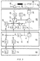
- FIG. 3 A second example is shown in FIG. 3. Here, too, is meant to be on means already described and signals are only received as far as it seems necessary.
- the output of the second dynamic memory 15 directly with the input of the correction memory 24 connected is.
- the output of an overlay 16 ' is connected to a third static memory (MS 3) 32, its exit to a third layer of superposition 33 leads. This is with another one Input with the output of the correction memory 24 connected and gives its output signal to the second Switching input of the switch 22.
- the function of the embodiment according to Figure 3 causes the offset correction values and the static correction values within the microprocessor 13 linked together and the specific Level 20 are supplied.
- the dynamic correction values of the memory 15 become the correction memory 24 fed. So when a drift appears, overall, a significantly reduced data flow was achieved become.
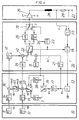
- FIG 4 is another embodiment shown, in which the deflection coil 28 is driven is controlled by two different control chains, the are formed by the digital-to-analog converter already mentioned 25 (drive chain A) and another Digital-to-analog converter 34 (drive chain B).
- a chain switch 35 selected which also by the electronic control unit 23 is controlled. through of the same signal will also be two more Switch 36, 37 driven, thereby saving or reading out those belonging to the individual chains Offset values is effected.
- Chain A is to be adjusted in the control mode switches 35, 36, 37 take the one Position shown in Figure 4.
- the offset values determined in this way are in the second Offset memory 21 and in an A offset memory (MO A) 39a read.
- the switches 35, 36, 37 assume an opposite position to that shown in FIG. 4 and the corresponding offset values are stored in the second offset memory 21 and the B offset memory (MO B) 39b stored.
- the mean value of the offset values of chain A and chain B is stored in an AB memory (M AB) 40, which is arranged between link 16 and link 16 ', ie 1/2 (offset (A) + offset (B)).
- Offset (A) and offset (B) are determined in Dependence on that stored in memory 31 Value as already described above.
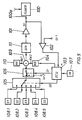
- Fig. 5 shows a circuit in which the correction of control variables at a receiver is used.
- a block called Tuner 100 contains in addition to the known levels of a receiver, for example for wireless or wired transmitted radio frequency or optical signals, also stages for the preparation of corresponding information such that they are a user or downstream Funds are made available can.
- a control input 100a of the tuner is both with the output of an amplifier 101 as well connected to a first input of a comparator 102.
- the comparator 102 is connected via a second input and a first reference signal Ur1 is supplied
- Output is with a control device (electronic control unit, ECU) 103.
- the control unit 103 outputs Signals to an operational correction value memory (MB) 104, a channel switch 105 and a test mode switch 106 onwards.
- Channel switching signals Sk and test mode switching signals St are formed by the ECU 103 depending on input signals that a User or means not shown via an input level 107 can specify.
- Inputs of the channel switch 105 are connected with station memories 108, each in digitally values for a frequency to be received are saved.
- the output of the channel switch 105 is connected to a switch input of the test mode switch 106, whose second switching input a second reference signal Ur2 is supplied.
- the Output of switch 106 leads to an addition stage 109, the additional first correction values Kw1 a fixed correction value memory 110 and second Correction values Kw2 are supplied from the memory 104 become.
- the output of addition stage 109 is connected with a digital / analog (D / A) converter 111, whose output signal is the input of the amplifier 101 is supplied.
- D / A digital / analog
- the control signal St is additionally in predetermined periods of time by means of the comparator 102 and the ECU 103 corrected. This is done by instead of of the output signals of the station memory 108 second reference signal Ur2 supplied to the addition stage 109 and the corresponding value of the control signal St is compared with the first reference signal Ur1.
Landscapes
- Engineering & Computer Science (AREA)
- Multimedia (AREA)
- Signal Processing (AREA)
- Video Image Reproduction Devices For Color Tv Systems (AREA)
- Analogue/Digital Conversion (AREA)
Claims (8)
- Méthode de correction d'image présentant deux phases distinctes, consécutives dans le temps, où
la première phase est une phase de réglage, qui comprend les étapes suivantes :où parmi les signaux de correction définis auparavant, un premier groupe (Ks) produit des corrections statiques et un second groupe (Kd) des corrections dynamiques, etpendant l'intervalle de suppression vertical, une valeur réelle (I) est déterminée, représentant une mesure pour le courant électrique passant dans un module de réglage (28),par suite, par une comparaison entre la valeur réelle (I) et une valeur de consigne donnée, un signal régulateur (Rs) est détecté, et ensuitepar une superposition du signal régulateur (Rs) avec des signaux de correction prédéfinis mémorisés (Ks, Kd), un signal de réglage (S) est produit,où la deuxième phase est une phase de fonctionnement pendant laquelle le signal de réglage (S) ou un signal dérivé (S") est mené au module de réglage (28),
où dans la phase de fonctionnement, le signal régulateur (Rs) est d'abord superposé aux signaux de correction définis pour les corrections statiques (Ks), ce par quoi un signal de décalage statique (Kso) est obtenu, et
où le signal de décalage statique (Kso) est ensuite superposé aux signaux de correction définis pour les corrections dynamiques (Kd), ce par quoi on obtient le signal de réglage (S). - Méthode selon la revendication 1, caractérisée en ce que d'autres signaux (M) sont superposés au signal régulateur (Rs) ou à un signal dérivé (Rs"), de sorte que la plage de valeurs du signal régulateur (Rs) soit réduite.
- Méthode selon la revendication 1 ou 2, caractérisée en ce que plus d'une chaíne de commande est affectée au module de réglage et pour chacune de ces chaínes de commande des signaux de réglage sont déterminés.
- Méthode selon la revendication 3, caractérisée en ce que les signaux suivants sont formés :que le signal de valeur moyenne (MAB) est superposé à la variable réglante statique etun signal de valeur moyenne (MAB) à partir des signaux régulateurs pour les chaínes de commande,des signaux différentiels à partir des signaux régulateurs et du signal de valeur moyenne (MAB),
que les signaux différentiels sont superposés au signal de réglage dynamique. - Dispositif de correctionavec un module de commutation (22, 23), au moyen duquel le dispositif est commutable soit sur un mode réglage, soit sur un mode fonctionnement,avec une chaíne de commande, au moyen de laquelle dans le mode fonctionnement, des signaux de correction prédéfinis mémorisés dans des premiers modules mémoire (11, 12) peuvent être amenés à des éléments de circuit électriques (22, 24, 25, 26) en tant que signaux d'entrée, qui délivrent un courant correspondant à chaque signal d'entrée à une bobine (28) en tant que composant de réglage,avec un module de mesure (29), qui détecte une valeur réelle,avec des modules de comparaison (18, 19, 30) qui comparent la valeur réelle mesurée avec une valeur de consigne et produisent un signal régulateur (Rs),et avec une mémoire (17), dans laquelle le signal régulateur (Rs) peut être enregistré pendant le mode réglage et de laquelle le signal régulateur (Rs) est extractible pendant le mode fonctionnement et peut être amené à la chaíne de commande, où le module de commutation (22, 23) est monté de telle sorte dans le circuit, que pendant le mode réglage, les valeurs de correction mémorisées dans les premiers modules mémoire (11, 12), n'influencent pas le composant de réglage (28), et où entre le composant de réglage et le module de mesure (29) un système réglé est formé comme une liaison conductrice électrique caractérisé en ce que
une troisième mémoire (31) est prévue, dans laquelle d'autres signaux sont enregistrés, signaux qui sont superposés au signal régulateur (Rs) ou à un signal dérivé (Rs"). - Dispositif selon la revendication 5, caractérisé en ce que plus d'une chaíne de commande (A, B) est affectée au module de réglage (28) et que les modules de commande (23) ont pour effet que pour chacune de ces chaínes de commande (A, B) des signaux de réglage sont déterminés.
- Dispositif selon la revendication 6, caractérisé en ce queun étage de valeur moyenne (40) est prévu, qui forme une valeur moyenne (MAB) à partir des signaux régulateurs des chaínes de commande et forme des signaux différentiels à partir des signaux régulateurs et du signal de valeur moyenne (MAB),un premier étage de superposition (16) est prévu, qui superpose le signal de valeur moyenne (MAB) à la variable réglante statique,un second étage de superposition (16') est prévu, qui superpose les signaux différentiels au signal de réglage dynamique.
- Téléviseur caractérisé en ce qu'il présente un dispositif selon une des revendications 5 à 7.
Applications Claiming Priority (2)
| Application Number | Priority Date | Filing Date | Title |
|---|---|---|---|
| DE4214317 | 1992-05-04 | ||
| DE4214317A DE4214317A1 (de) | 1992-05-04 | 1992-05-04 | Verfahren und Vorrichtung zur Regelung |
Publications (3)
| Publication Number | Publication Date |
|---|---|
| EP0568982A1 EP0568982A1 (fr) | 1993-11-10 |
| EP0568982B1 EP0568982B1 (fr) | 2000-06-07 |
| EP0568982B2 true EP0568982B2 (fr) | 2004-01-14 |
Family
ID=6457879
Family Applications (1)
| Application Number | Title | Priority Date | Filing Date |
|---|---|---|---|
| EP93107232A Expired - Lifetime EP0568982B2 (fr) | 1992-05-04 | 1993-05-04 | Méthode et dispositif de correction d'image numérique |
Country Status (5)
| Country | Link |
|---|---|
| US (1) | US5488271A (fr) |
| EP (1) | EP0568982B2 (fr) |
| DE (2) | DE4214317A1 (fr) |
| ES (1) | ES2148194T5 (fr) |
| SG (1) | SG45448A1 (fr) |
Families Citing this family (5)
| Publication number | Priority date | Publication date | Assignee | Title |
|---|---|---|---|---|
| DE19801968A1 (de) * | 1998-01-21 | 1999-07-22 | Thomson Brandt Gmbh | Verfahren und Vorrichtung zur Konvergenzkorrektur in einem Fernsehgerät |
| DE19801966A1 (de) * | 1998-01-21 | 1999-07-22 | Thomson Brandt Gmbh | Einrichtung zur Konvergenzkorrektur in einem Fernsehgerät |
| DE19927782A1 (de) | 1999-06-18 | 2000-12-21 | Thomson Brandt Gmbh | Schaltung zur Korrektur von Ablenkfehlern in einem Fernsehgerät |
| US6473139B1 (en) | 1999-09-30 | 2002-10-29 | Thomson Licensing S.A. | Data error recovery for digital beam landing error correction arrangement |
| US6369780B2 (en) | 1999-09-30 | 2002-04-09 | Thomson Licensing S.A. | Auxiliary deflection winding driver disabling arrangement |
Family Cites Families (18)
| Publication number | Priority date | Publication date | Assignee | Title |
|---|---|---|---|---|
| US3996611A (en) * | 1974-09-25 | 1976-12-07 | Aeronutronic Ford Corporation | Cathode ray tube deflection circuit |
| SU930743A1 (ru) * | 1976-12-29 | 1982-05-23 | Предприятие П/Я В-2645 | Корректор растровых искажений видеосигнала |
| US4422019A (en) * | 1982-07-12 | 1983-12-20 | Tektronix, Inc. | Apparatus for providing vertical as well as horizontal smoothing of convergence correction signals in a digital convergence system |
| DE3439927A1 (de) * | 1984-06-30 | 1986-01-09 | Bosch Gmbh Robert | Verfahren und vorrichtung zur adaptiven stoergroessenaufschaltung bei reglern |
| JPS6178294A (ja) * | 1984-09-25 | 1986-04-21 | Sony Corp | デイジタルコンバ−ジエンス補正装置 |
| JPS61281791A (ja) * | 1985-06-07 | 1986-12-12 | Sony Corp | デイジタルコンバ−ジエンス装置 |
| CA1294702C (fr) * | 1987-02-26 | 1992-01-21 | Teruo Kataoka | Dispositif automatique d'alignement de la convergence des couleurs primaires pour televiseur a projection |
| US4870329A (en) * | 1987-02-27 | 1989-09-26 | Nippon Gijutsu Boeki Co., Ltd. | Digital convergence circuit storing coefficients of fundamental waves of correction data |
| DE3716259A1 (de) * | 1987-05-15 | 1988-11-24 | Eckardt Ag | Verfahren zur regelung einer wenigstens zwei zu- und/oder abschaltbare verbraucher beaufschlagenden prozessgroesse eines verfahrenstechnischen prozesses, insbesondere fuer eine druckregelung eines brenner- oder heizsystems |
| DE3804480A1 (de) * | 1988-02-12 | 1989-08-24 | Siemens Ag | Ablenkschaltung |
| JP3035912B2 (ja) * | 1988-10-14 | 2000-04-24 | ソニー株式会社 | 画像表示の補正波形データ生成装置 |
| US4990834A (en) * | 1988-12-23 | 1991-02-05 | U.S. Philips Corporation | Line deflection circuit arrangement for a picture display device |
| US4935674A (en) * | 1988-12-27 | 1990-06-19 | Rca Licensing Corporation | Digitally controlled convergence system |
| US4956586A (en) * | 1989-03-03 | 1990-09-11 | Hewlett-Packard Company | Frequency independent CRT horizontal sweep generator having current feedback and improved pincushion correction circuitry |
| JPH02311889A (ja) * | 1989-05-29 | 1990-12-27 | Hitachi Ltd | 高安定垂直偏向回路 |
| DE3933950A1 (de) * | 1989-10-11 | 1991-04-18 | Thomson Brandt Gmbh | Einrichtung zur rasterkorrektur in einem fernsehgeraet |
| DE3943421A1 (de) * | 1989-12-30 | 1991-07-04 | Thomson Brandt Gmbh | Schaltung zur rasterkorrektur in einem fernsehgeraet |
| US5107190A (en) * | 1990-06-22 | 1992-04-21 | Motorola, Inc. | Means and method for optimizing the switching performance of power amplifiers |
-
1992
- 1992-05-04 DE DE4214317A patent/DE4214317A1/de not_active Withdrawn
-
1993
- 1993-05-04 DE DE59310054T patent/DE59310054D1/de not_active Expired - Fee Related
- 1993-05-04 EP EP93107232A patent/EP0568982B2/fr not_active Expired - Lifetime
- 1993-05-04 SG SG1996008945A patent/SG45448A1/en unknown
- 1993-05-04 ES ES93107232T patent/ES2148194T5/es not_active Expired - Lifetime
-
1995
- 1995-04-14 US US08/422,741 patent/US5488271A/en not_active Expired - Fee Related
Non-Patent Citations (4)
| Title |
|---|
| Datenblatt "Ablenkprozessor SDA 9064" der Firma Siemens, Ausgabe 9.87 † |
| Fernsehgeräte der Firma Metz mit den Chassis 689 G-..., Mallorca 84-100 VT 7994, Tahiti 70-100 VT 7999 und zugehörige Broschüre "Technik und Service", Seiten 35-40 und Tafel 2 † |
| Tagungsvorlage "Digitalchassis DIV A3B", Dokumentation der Siemens AG, BV AT UE S2, vom 23.02.1988, präsentiert und übergeben Herrn Ing. Heinz Kraus 1988 anlässlich einer Präsentation des Systems bei Siemens. "ICs for Entertainment Electronics", Edition 8.87, Seiten 3-10, sowie die Figuren 1-4 † |
| Valvo Druckschrift "Die Videokombination TDA 4580, TI 850719", Seiten 14/15 † |
Also Published As
| Publication number | Publication date |
|---|---|
| DE4214317A1 (de) | 1993-11-11 |
| SG45448A1 (en) | 1998-01-16 |
| US5488271A (en) | 1996-01-30 |
| EP0568982B1 (fr) | 2000-06-07 |
| DE59310054D1 (de) | 2000-07-13 |
| ES2148194T3 (es) | 2000-10-16 |
| EP0568982A1 (fr) | 1993-11-10 |
| ES2148194T5 (es) | 2004-07-16 |
Similar Documents
| Publication | Publication Date | Title |
|---|---|---|
| DE10101065B4 (de) | Elektronisches Endoskopsystem und Selektor hierfür | |
| AT398506B (de) | Signalverarbeitungsschaltung | |
| DE3942736B4 (de) | Signalformgenerator zur Erzeugung mehrerer Ablenksignalformen | |
| DE69513716T2 (de) | Fernsehempfänger mit Bild-in-Bild | |
| DE3045541C2 (fr) | ||
| EP0568982B2 (fr) | Méthode et dispositif de correction d'image numérique | |
| DE3744110C2 (fr) | ||
| EP1125428B1 (fr) | Circuit permettant de transformer un debit binaire | |
| DE19611059A1 (de) | Verfahren zur Signalgewinnung in elektronischen Geräten mittels Interpolation zwischen Stützstellenwerten | |
| DE1293822B (de) | System zur Wiedergabe aufgezeichneter Farbfernsehsignale mit genauer Zeitbasisstabilitaet | |
| DE2623745A1 (de) | Schaltungsanordnung mit einem ladungsgekoppelten element | |
| EP0443064B1 (fr) | Dispositif d'insertion d'une première image dans une deuxième image sur un écran | |
| DE3722092C2 (de) | Video-Wiedergabegerät | |
| EP0596561B1 (fr) | Dispositif de doublement de la fréquence de trame d'un signal d'image | |
| DE19801968A1 (de) | Verfahren und Vorrichtung zur Konvergenzkorrektur in einem Fernsehgerät | |
| DE69930559T2 (de) | Schaltung zur Konvergenzkorrektur in einem Fernsehempfänger | |
| DE19650524A1 (de) | Doppelabstimmschaltung für TV-Tuner | |
| AT392713B (de) | Schaltungsanordnung zur zufuhr von ablenksteuersignalen zu den horizontal- bzw. vertikalablenkeinrichtungen in einer mehrroehren-fernsehkamera | |
| EP0135035B1 (fr) | Procédé et circuit pour le perfectionnement de la qualité d'une image de télévision | |
| DE836045C (de) | System zur UEbertragung elektrischer Signale mit wiederkehrenden Festpegel- oder Bezugswerten | |
| DE3419645A1 (de) | Transversalfilter mit mos-transistor-verstaerkern | |
| EP0621729B1 (fr) | Dispositif de visualisation sur écran d'une première image dans une seconde image | |
| DE19754905C2 (de) | Verfahren und Vorrichtung zur Kathodenstrahlröhren-Fokussierungskorrektur, und zugehörige Anzeigeeinheit | |
| DE3429264C2 (de) | Fernsehkameraschaltung zur Korrektur einer Farb-, bzw. Helligkeitsverschiebung | |
| EP0697790A2 (fr) | Procédé et circuit d'insertion d'image dans l'image |
Legal Events
| Date | Code | Title | Description |
|---|---|---|---|
| PUAI | Public reference made under article 153(3) epc to a published international application that has entered the european phase |
Free format text: ORIGINAL CODE: 0009012 |
|
| AK | Designated contracting states |
Kind code of ref document: A1 Designated state(s): DE ES FR GB IT |
|
| 17P | Request for examination filed |
Effective date: 19940509 |
|
| 17Q | First examination report despatched |
Effective date: 19960726 |
|
| GRAG | Despatch of communication of intention to grant |
Free format text: ORIGINAL CODE: EPIDOS AGRA |
|
| GRAG | Despatch of communication of intention to grant |
Free format text: ORIGINAL CODE: EPIDOS AGRA |
|
| GRAG | Despatch of communication of intention to grant |
Free format text: ORIGINAL CODE: EPIDOS AGRA |
|
| GRAH | Despatch of communication of intention to grant a patent |
Free format text: ORIGINAL CODE: EPIDOS IGRA |
|
| GRAH | Despatch of communication of intention to grant a patent |
Free format text: ORIGINAL CODE: EPIDOS IGRA |
|
| GRAA | (expected) grant |
Free format text: ORIGINAL CODE: 0009210 |
|
| AK | Designated contracting states |
Kind code of ref document: B1 Designated state(s): DE ES FR GB IT |
|
| GBT | Gb: translation of ep patent filed (gb section 77(6)(a)/1977) |
Effective date: 20000608 |
|
| REF | Corresponds to: |
Ref document number: 59310054 Country of ref document: DE Date of ref document: 20000713 |
|
| ET | Fr: translation filed | ||
| ITF | It: translation for a ep patent filed | ||
| REG | Reference to a national code |
Ref country code: ES Ref legal event code: FG2A Ref document number: 2148194 Country of ref document: ES Kind code of ref document: T3 |
|
| PLBQ | Unpublished change to opponent data |
Free format text: ORIGINAL CODE: EPIDOS OPPO |
|
| PLBI | Opposition filed |
Free format text: ORIGINAL CODE: 0009260 |
|
| PLBF | Reply of patent proprietor to notice(s) of opposition |
Free format text: ORIGINAL CODE: EPIDOS OBSO |
|
| 26 | Opposition filed |
Opponent name: INTERESSENGEMEINSCHAFT FUER RUNDFUNKSCHUTZRECHTE G Effective date: 20010307 |
|
| PLBF | Reply of patent proprietor to notice(s) of opposition |
Free format text: ORIGINAL CODE: EPIDOS OBSO |
|
| REG | Reference to a national code |
Ref country code: GB Ref legal event code: 746 Effective date: 20010803 |
|
| PLBF | Reply of patent proprietor to notice(s) of opposition |
Free format text: ORIGINAL CODE: EPIDOS OBSO |
|
| REG | Reference to a national code |
Ref country code: FR Ref legal event code: D6 |
|
| REG | Reference to a national code |
Ref country code: GB Ref legal event code: IF02 |
|
| PLBF | Reply of patent proprietor to notice(s) of opposition |
Free format text: ORIGINAL CODE: EPIDOS OBSO |
|
| PLAW | Interlocutory decision in opposition |
Free format text: ORIGINAL CODE: EPIDOS IDOP |
|
| PUAH | Patent maintained in amended form |
Free format text: ORIGINAL CODE: 0009272 |
|
| 27A | Patent maintained in amended form |
Effective date: 20040114 |
|
| AK | Designated contracting states |
Kind code of ref document: B2 Designated state(s): DE ES FR GB IT |
|
| REG | Reference to a national code |
Ref country code: ES Ref legal event code: DC2A Date of ref document: 20040220 Kind code of ref document: T5 |
|
| ET3 | Fr: translation filed ** decision concerning opposition | ||
| PGFP | Annual fee paid to national office [announced via postgrant information from national office to epo] |
Ref country code: GB Payment date: 20050412 Year of fee payment: 13 |
|
| PGFP | Annual fee paid to national office [announced via postgrant information from national office to epo] |
Ref country code: DE Payment date: 20050517 Year of fee payment: 13 |
|
| PGFP | Annual fee paid to national office [announced via postgrant information from national office to epo] |
Ref country code: FR Payment date: 20050524 Year of fee payment: 13 |
|
| PGFP | Annual fee paid to national office [announced via postgrant information from national office to epo] |
Ref country code: ES Payment date: 20050531 Year of fee payment: 13 |
|
| PG25 | Lapsed in a contracting state [announced via postgrant information from national office to epo] |
Ref country code: GB Free format text: LAPSE BECAUSE OF NON-PAYMENT OF DUE FEES Effective date: 20060504 |
|
| PG25 | Lapsed in a contracting state [announced via postgrant information from national office to epo] |
Ref country code: ES Free format text: LAPSE BECAUSE OF NON-PAYMENT OF DUE FEES Effective date: 20060505 |
|
| PGFP | Annual fee paid to national office [announced via postgrant information from national office to epo] |
Ref country code: IT Payment date: 20060531 Year of fee payment: 14 |
|
| PG25 | Lapsed in a contracting state [announced via postgrant information from national office to epo] |
Ref country code: DE Free format text: LAPSE BECAUSE OF NON-PAYMENT OF DUE FEES Effective date: 20061201 |
|
| GBPC | Gb: european patent ceased through non-payment of renewal fee |
Effective date: 20060504 |
|
| REG | Reference to a national code |
Ref country code: FR Ref legal event code: ST Effective date: 20070131 |
|
| REG | Reference to a national code |
Ref country code: ES Ref legal event code: FD2A Effective date: 20060505 |
|
| PG25 | Lapsed in a contracting state [announced via postgrant information from national office to epo] |
Ref country code: FR Free format text: LAPSE BECAUSE OF NON-PAYMENT OF DUE FEES Effective date: 20060531 |
|
| PG25 | Lapsed in a contracting state [announced via postgrant information from national office to epo] |
Ref country code: IT Free format text: LAPSE BECAUSE OF NON-PAYMENT OF DUE FEES Effective date: 20070504 |