EP0621985B1 - Montage d'un systeme de connexion miniature - Google Patents
Montage d'un systeme de connexion miniature Download PDFInfo
- Publication number
- EP0621985B1 EP0621985B1 EP92905232A EP92905232A EP0621985B1 EP 0621985 B1 EP0621985 B1 EP 0621985B1 EP 92905232 A EP92905232 A EP 92905232A EP 92905232 A EP92905232 A EP 92905232A EP 0621985 B1 EP0621985 B1 EP 0621985B1
- Authority
- EP
- European Patent Office
- Prior art keywords
- contacts
- housing
- circuit board
- contact
- holes
- Prior art date
- Legal status (The legal status is an assumption and is not a legal conclusion. Google has not performed a legal analysis and makes no representation as to the accuracy of the status listed.)
- Expired - Lifetime
Links
- 238000000034 method Methods 0.000 claims abstract description 14
- 238000009434 installation Methods 0.000 claims abstract description 12
- 125000006850 spacer group Chemical group 0.000 claims description 6
- 239000000463 material Substances 0.000 claims description 4
- 239000002184 metal Substances 0.000 description 5
- 229910052751 metal Inorganic materials 0.000 description 5
- 229920001169 thermoplastic Polymers 0.000 description 5
- 239000004416 thermosoftening plastic Substances 0.000 description 5
- 230000000712 assembly Effects 0.000 description 4
- 238000000429 assembly Methods 0.000 description 4
- 229920001875 Ebonite Polymers 0.000 description 2
- 229910000831 Steel Inorganic materials 0.000 description 2
- 238000003780 insertion Methods 0.000 description 2
- 230000037431 insertion Effects 0.000 description 2
- 239000010959 steel Substances 0.000 description 2
- 229910000906 Bronze Inorganic materials 0.000 description 1
- 239000010974 bronze Substances 0.000 description 1
- KUNSUQLRTQLHQQ-UHFFFAOYSA-N copper tin Chemical compound [Cu].[Sn] KUNSUQLRTQLHQQ-UHFFFAOYSA-N 0.000 description 1
- 230000005484 gravity Effects 0.000 description 1
- 230000013011 mating Effects 0.000 description 1
- 150000002739 metals Chemical class 0.000 description 1
- 238000012986 modification Methods 0.000 description 1
- 230000004048 modification Effects 0.000 description 1
- 239000012815 thermoplastic material Substances 0.000 description 1
Images


Classifications
-
- H—ELECTRICITY
- H01—ELECTRIC ELEMENTS
- H01R—ELECTRICALLY-CONDUCTIVE CONNECTIONS; STRUCTURAL ASSOCIATIONS OF A PLURALITY OF MUTUALLY-INSULATED ELECTRICAL CONNECTING ELEMENTS; COUPLING DEVICES; CURRENT COLLECTORS
- H01R12/00—Structural associations of a plurality of mutually-insulated electrical connecting elements, specially adapted for printed circuits, e.g. printed circuit boards [PCB], flat or ribbon cables, or like generally planar structures, e.g. terminal strips, terminal blocks; Coupling devices specially adapted for printed circuits, flat or ribbon cables, or like generally planar structures; Terminals specially adapted for contact with, or insertion into, printed circuits, flat or ribbon cables, or like generally planar structures
- H01R12/50—Fixed connections
- H01R12/51—Fixed connections for rigid printed circuits or like structures
- H01R12/55—Fixed connections for rigid printed circuits or like structures characterised by the terminals
- H01R12/58—Fixed connections for rigid printed circuits or like structures characterised by the terminals terminals for insertion into holes
-
- H—ELECTRICITY
- H01—ELECTRIC ELEMENTS
- H01R—ELECTRICALLY-CONDUCTIVE CONNECTIONS; STRUCTURAL ASSOCIATIONS OF A PLURALITY OF MUTUALLY-INSULATED ELECTRICAL CONNECTING ELEMENTS; COUPLING DEVICES; CURRENT COLLECTORS
- H01R43/00—Apparatus or processes specially adapted for manufacturing, assembling, maintaining, or repairing of line connectors or current collectors or for joining electric conductors
- H01R43/20—Apparatus or processes specially adapted for manufacturing, assembling, maintaining, or repairing of line connectors or current collectors or for joining electric conductors for assembling or disassembling contact members with insulating base, case or sleeve
- H01R43/205—Apparatus or processes specially adapted for manufacturing, assembling, maintaining, or repairing of line connectors or current collectors or for joining electric conductors for assembling or disassembling contact members with insulating base, case or sleeve with a panel or printed circuit board
-
- H—ELECTRICITY
- H01—ELECTRIC ELEMENTS
- H01R—ELECTRICALLY-CONDUCTIVE CONNECTIONS; STRUCTURAL ASSOCIATIONS OF A PLURALITY OF MUTUALLY-INSULATED ELECTRICAL CONNECTING ELEMENTS; COUPLING DEVICES; CURRENT COLLECTORS
- H01R13/00—Details of coupling devices of the kinds covered by groups H01R12/70 or H01R24/00 - H01R33/00
- H01R13/40—Securing contact members in or to a base or case; Insulating of contact members
- H01R13/405—Securing in non-demountable manner, e.g. moulding, riveting
- H01R13/41—Securing in non-demountable manner, e.g. moulding, riveting by frictional grip in grommet, panel or base
Definitions
- SCEM small computer expendability module
- SCEM small computer expendability module
- SCEM small computer expendability module
- a connector must lie within a circuit board area of about 76.2 mm by 8.5 mm (three inches by one third inch).
- the connector has 400 contacts arranged in six rows in a small area. As a result, the contact centers must be spaced apart along each row by about one millimeter, necessitating the use of very small contacts. A method for installing such large number of miniature contacts reliably and at low cost, would be of considerable value.
- a method for installing large numbers of contacts of a connector in holes of a circuit board, and a combination of a connector assembly and a circuit board according to claim 7, constructed to facilitate such installation, are provided, enabling installation accurately and at low cost.
- the method applies to a connector assembly on a circuit board, wherein said circuit board has a plurality of rows of holes and said connector assembly includes an upper housing with a base that has a plurality of rows of holes and a plurality of contacts with upper end portions for lying in said plurality of rows in said housing and a mount portion, with each mount portion constructed for interference fit into one of said circuit board holes, using contacts with said contact mount portions formed with a largely upward-facing shoulder, futher using an upper housing with a base formed with largely downwardly-facing lower surface regions around each of said contact receiving holes.
- the method includes first, installing each said contact upper end portion into one of said housing holes so said upward-facing shoulder of said contact mount portion is spaced below the level of a corresponding one of said downwardly-facing lower surface regions to leave a space between them as seen in a side view, temporarily installing at least one push bar between a plurality of said upward-facing shoulders and said housing surface regions, so said push bar can engage both said upward-facing shoulders and said downward-facing surface regions; with said mount portions lying above and aligned with said circuit board holes, pressing down against said upper housing and transmitting force via said upper housing from said lower surface regions through said push bar to said upward-facing shoulders, to simultaneously press down said mount portions into said circuit board holes, finaly removing said push bar from between said contact shoulders and said housing lower surface regions.
- an aligner is pressed sidewardly against each contact lower portion to deflect it into alignment with a corresponding circuit board hole.
- Each aligner is preferably in the form of a bar having a greater width than thickness.
- the aligner bar is initially installed with its width vertical, and thereafter the aligner bar is turned so its width is horizontal to deflect apart adjacent contact lower ends.
- the lower end portions of the contact once projecting from the lower surface of the circuit board, can be installed in a lower housing which has a tapered deflector projecting from its upper surface to deflect the tips of the contact slightly sidewardly into holes of the lower housing.
- Fig. 1 is an exploded isometric view of a connector system for connecting modules of an expandable module system.
- Fig. 2 is a partial isometric view of the system of Fig. 1, showing three circuit boards and associated connectors.
- Fig. 3 is a sectional view of two connectors and two associated circuit boards of the system of Fig. 2, shown in a fully mated position.
- Fig. 4 is a partial isometric view of one of the connector assemblies of Fig. 3, with modified end portions.
- Fig. 5 is a partial sectional view of one of the connector systems of Fig. 3.
- Fig. 6 is a view taken on the line 6 - 6 of Fig. 5.
- Fig. 7 is a view taken on the line 7 - 7 of Fig. 5.
- Fig. 8 is a partial plan view of one of the circuit boards of Fig. 3, shown prior to installation of connector housings and contacts therein.
- Figs. 9A - 9H are sectional views of one of the connector assemblies of Fig. 3, showing various stages in the installation of the contacts in the circuit board and in the lower connector housing.
- Fig. 10 is a sectional view of the lower housing of one of the connector assemblies of Fig. 3, shown prior to installation of contacts therein.
- Fig. 11 is a view taken on the line 11 - 11 of Fig. 10.
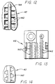
- Fig. 12 is an enlarged view of a portion of Fig. 11.
- Fig. 13 is a view taken on the line 13 - 13 of Fig. 10.
- Fig. 14 is an enlarged view of a portion of Fig. 13.
- Fig. 15 is a simplified isometric view of apparatus used in the installation steps of Figs 9A - 9H.
- Fig. 16 is a side elevation view of additional apparatus used in the installation steps shown in Fig. 9F.
- Fig. 1 illustrates a connector system 10 for connecting various modules 12, 14, 16 to each other and to a module in the form of a mother board 18.
- This type of architecture has been designed for use with small computers to allow modules to expand the capability of the computer.
- Each module 12 - 16 includes a module connector assembly 22 - 26 for interconnecting the modules to each other and to a connector 20 on the mother board.
- Each of the middle module connectors 22, 24 includes upper and lower housings 30, 32 at opposite faces of the circuit board 34, and multiple contacts extending through the circuit board and into each of the housings 30, 32.
- Each of the end module connectors 20, 26 has a connector housing on only one side of the corresponding circuit board.
- terms such as “upper”, “lower”, “vertical”, etc. are used only to aid in the description of the invention, and the system can be used in any orientation with respect to gravity.
- Fig. 2 shows an arrangement which includes only the mother board 18 and two of the modules 12, 16.
- Fig. 3 illustrates an arrangement that includes only the two uppermost modules 14, 16 and their corresponding connector assemblies 24, 26. Any of the above arrangements and more complex ones can be used.
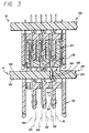
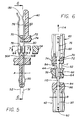
- the connector assembly 24 includes upper and lower connector housings 40, 42 lying respectively against upper and lower surfaces 44, 46 of the circuit board 34.
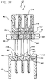
- a large number of contacts 50 are arranged in six rows 51 - 56.
- Each contact has an upper end portion 60 that lies primarily within the upper housing 40, a lower end portion 62 lying primarily within the lower housing 42 and a mount portion 64 lying within a hole 66 of the circuit board in interference fit, or press fit therein.
- the mount portion forms an upwardly-facing shoulder 78 which is used in installing the contact in the circuit board hole.
- the holes 66 of the circuit board which lie in the six rows 51 - 56, are staggered, in that one column 70 of holes includes holes in only three of the rows (rows 51, 53, and 55) while the next adjacent column of holes 72 includes holes only in each of the other three rows (rows 52, 54, and 56).
- a sectional view of the connector assembly may show only portions of contacts in only three rows, with corresponding portions of contacts in the other three rows being hidden.
- Fig. 5 which shows two contacts 50A, 50B
- a simple sectional view that would show all of contact 50B would show only part of the other contact 50A.
- the upper end portion 60 includes a base-received part 70 that lies in interference fit with the walls of a hole 72 in the base 74 of the upper housing 40.
- the upper end portion 60 also includes a beam 76 which can engage a contact of another connector assembly.
- the upper end portion 60 also includes an unenclosed or bare part 80 which lies in the space 82 between the upper surface 44 of the circuit board and the lower surface portion 84 of the upper housing that lies immediately around the contact.
- the space 82 has a thickness Y which is much more than the average thickness A of each contact end portion.
- the contact also has a lower end portion 90 with a lower tip 92 lying within the lower housing 42 and a base-received portion 94 lying in interference fit with the walls of a hole 96 in the lower housing.
- the interference fit between a contact mount portion 64 and a corresponding circuit board hole 66 is a high interference fit, in that this interference fit is the primary means for holding the contact in position, such as against upward and downward forces applied during mating and unmating from contacts of other connectors.
- the center-to-center spacing of contacts along each row was one millimeter.
- Each contact was constructed of sheet metal having a thickness of 0.15 mm (six thousandths inch) and a width B of 0.38 mm (fourteen thousandths inch). Yet, the insertion force required to push the mount portion 64 into the circuit board hole 66, (which was metal plated) was between 2.72 to 5.44 kg (six to twelve pounds).
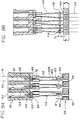
- a large number of contacts to be installed in a single row are formed simultaneously from a sheet of metal, with the mount portions 64 of all contacts bent to a "C" shape as shown in Fig. 7, and with the upper and lower end portions bent as shown.
- Different positions of the contact end portions such as 60 with respect to the "C" shaped mount portion 64 can be utilized.
- Figs. 5 - 7 show a latest and preferred position. As shown in Fig. 7, the contact upper end portion 60 extends from one side 67 of the upwardly-facing shoulder 78, while the space immediately above the other side 68 of the shoulder is unobstructed.
- a bar portion of the width X lying over the shoulder will pres down against about two-thirds of the cross-section of the mount portion 64.
- the row of contacts With the row of contacts still part of a single sheet by virtue of connector parts (not shown) connecting them to a carrier strip of the sheet metal, the row of contacts are inserted into the row of holes 72 (Fig. 5) in the upper housing 40, this requiring only moderate force, and with each contact being individually accessible, at least from the bottom of the contact. After the rows of contacts have been installed in the upper housing 40, the contacts are severed from the carrier strip. The contacts are now to be installed in tight interference fit with the circuit board holes.
- Fig. 9A shows the connector assembly with the upper end portions 60 of the contacts installed in the upper housing 40, and with the contact lower end portions 62 extending down so their lower tips 100 lie at or slightly above the upper surface 44 of the circuit board 34.
- each tip 100 lie substantially on the axis 110 of the corresponding hole.
- the tips 100 are slightly spaced from the axis 110.
- Applicant installs elongated aligners or aligner bars 120 between the contacts in adjacent rows such as 51 and 52, slightly above the tips 100 of the contacts.
- Each aligner bar has a greater width W than its thickness T (Fig. 9B).
- Each of the aligner bars is rotatable about an axis 114 extending along the length of the aligner bar and parallel to the contact rows. The aligner bars are initially installed in the orientation shown in Fig. 9A with their widths vertical. As shown in Fig.
- the aligner bars are then rotated 90° so their widths are horizontal, and each aligner bar deflects a location 116 on the contact lower end portion 62 lying closer to the tip 100 than to the mount, so the tip lies aligned with the axis 110 of the cylindrical board hole.
- a next step is to lower the upper housing 40 by a very small amount, so that the lower tips 100 of the contact actually lie within the board holes 66.
- the aligner bars 120 are moved horizontally parallel to the lengths of the rows, to withdraw the aligner bars from between the contacts.
- Fig. 9D shows the apparatus with the aligner bars removed, but with the contact lower tips 100 lying within the board holes 66 so the contact tips will remain in the board holes.
- Fig. 9E shows a next step, which involves pushing down the upper housing 40 by a considerable amount (e.g. 12.7 mm (one-half inch)) until the contact mount portion lie substantially against the upper surface 44 of the circuit board, and ready to be inserted into the circuit board holes 66.
- Fig. 9F shows a next step, where a large downward force F is applied to the upper surface 124 of the upper housing 40 to push down the upper housing 40.
- the housing 40 presses down the push bars 102 - l06 which press down the mount portions 64 into the contact holes 66.
- the upper housing 40 is preferably molded of a thermoplastic chosen to have a moderately high strength for a thermoplastic, but whose strength is low compared to that of common metals such as bronze or steel. If the entire downward force of perhaps 2.7 to 5.4 kg (six to twelve pounds) per contact had to be applied directly by the lower surface of the thermoplastic upper housing 40, then there could be high pressure on the lower surface of the thermoplastic upper housing 40 which might damage it and result in one or more of the contacts not being pressed reliably into a circuit board hole. Also, as shown in Fig.
- the hole 72 in the housing base be considerably wider than the contact to enable a curved tip portion 130 to pass therethrough, which would result in only a small area of the housing pressing down against the shoulder 78 of the mount portion. There would even be danger that the C-shaped mount portion could be deformed into the housing hole 72.
- the use of the push bars such as 106 enables the use of a harder material, such as steel than the thermoplastic material of the housing. Also, the push bar 106 can lie over most of the shoulder 78, except for one side from which the upper contact portion 60 extends, to provide a large area of contact. The downward force applied to the push bars, is applied through the upper housing 40, by a large force F (Fig.
- the upper housing 40 is pushed down far enough until spacer legs 132 at the bottom of the housing lie substantially against the upper surface 44 of the circuit board.
- the spacer legs 132 position the upper housing stably on the circuit board.
- the upper housing 40 can be held down to the circuit board solely by the contacts, although separate fasteners can be used.
- the lower housing has a base 140 with base holes 142 which receive the contact lower end portions. However, the contact lower tips 100 are offset from the base holes 142.
- Applicant forms the lower housing 42 with tapered deflectors 144 extending upwardly from most of the housing upper surface 146 (the portion of the upper surface that lies between spacer legs 148 of the lower housing). As the lower housing 42 is moved upwardly, the contact tips engage inclined deflect surfaces 143 of tapered deflectors 144 and are deflected slightly to one side and into the base holes 142.
- FIG. 9G shows the connector assembly 24 with all parts thereof installed on the circuit board 34.
- the presser bars 106 are then removed by sliding them horizontally and parallel to the length of the contact rows, out of the space between the upper housing and the upper surface of the circuit board.
- Fig. 9H shows the connector assembly 24 with all installing apparatus removed.
- Fig. 15 is a simplified view of one apparatus 150 which can be used to insert and remove the push bars 102 - 104, and to insert, turn, and remove the aligner bars 120.
- the apparatus includes a guide device 152 having three rectangular guideways 154 that can guide the push bars 102 - 106 to move them between the bottom of the upper housing and the shoulders of the contact mount portions. Each bar has a tapered forward end 156 to facilitate its insertion.
- the guide member also has three cylindrical guideways 160 that each receives one of the alignment bars 120.
- the rear end of each alignment bar is fixed to a cylindrical rod 162 that can slide and rotate within one of the cylindrical guideways 160.
- the guide device 152 can slide up and down a short distance on a base 164 which guides the guide device 152 in vertical movement.
- the base 164 has positioning devices 166 with pins 168 that can be received in corresponding holes 170 (Fig. 8) of the circuit board to accurately align the base 164 with the circuit board.
- the upper housing 40 (Fig. 9A) with the upper contact end portions installed thereon, can be installed on the push bars 102 and alignment bars 120 by sliding the housing with contacts thereon horizontally over the bars.
- the aligner bars 120 are then turned to the position shown in Fig. 9B.
- the guide device 152 is moved downwardly a short distance such as several 0.025 mm (thousands inch), to the position shown in Fig. 9C, so the lower tips df the contacts enter the circuit board holes.
- the alignment bars 120 (Fig. 15) can then be turned, or can be left in their position, and then pulled rearwardly in the direction R out of the guide device 152.
- the guide device is then moved downwardly by a distance such as 12.7 mm (one-half inch), until the contacts and upper housing are at the position shown in Fig. 9E. If the guide device 152 is not to be used to apply large downward pressure to the upper housing, then the push bars 102 - 106 can be pushed further forward in the direction F, as by other bars 170 until the rear ends 172 of the push bar have been pushed forward of the guideways 154.
- Fig. 16 shows a next step, wherein the upper housing 40 with contacts 50 installed therein, and with the push bars such as 106 still in place, is installed between the piston 180 and anvil 182 of a press 184 that can apply forces of up to a few tons.
- the circuit board lies on a support 186 which supports locations on the circuit board immediately beyond opposite sides of the six rows of contacts.
- a hard rubber plate 190 has been placed on the upper surface 124 of the connector housing 40 to assure that downward forces on the upper surface 124 are uniformly distributed thereon, the hard rubber plate 190 being softer than the more rigid material of the thermoplastic housing 40.
- the press is then operated to move down the piston 180 to press fit the contact mount portions 64 into the circuit board holes.
- the invention provides a method for the installation of large numbers of miniature contacts in interference fit with a circuit board according to claim 1, and a combination of a connector assembly and a circuit board according to claim 7, constructed to facilitate such installation.
- the method includes using each contact mount portion with a largely upwardly-facing shoulder, and using an upper housing with a largely downwardly-facing surface region spaced above the shoulders.
- a push bar is installed between the contact shoulders and housing surface region so downward force on the top of the housing can be transmitted through the push bar to the shoulder of the mount portion to apply a large downward force to the mount portion that press fits it into a circuit board hole.
- the push bars can be installed in a direction parallel to the rows of contacts, and preferably with each push bar lying against shoulders of contacts lying in two adjacent rows.
- the lower tips of the contacts can be pushed into accurate alignment with circuit board holes, by an aligner that presses against a contact location closer to the lower tip of the contact than to the mount portion.
- Each aligner can be in the form of a bar having a greater width than thickness, and which is installed with its width dimension vertical, and which is then turned so its width dimension is horizontal to deflect a pair of contact locations apart.
- a lower housing can be inserted onto the lower end portions of the contacts that project from the lower surface of the circuit board, by moving the lower housing upwardly with respect to the circuit board and upper housing contacts thereon.
- the lower housing has an upper surface with tapered deflectors that deflect the tip of each contact sidewardly into one of the lower housing holes.
Landscapes
- Engineering & Computer Science (AREA)
- Manufacturing & Machinery (AREA)
- Coupling Device And Connection With Printed Circuit (AREA)
- Manufacturing Of Electrical Connectors (AREA)
- Connector Housings Or Holding Contact Members (AREA)
Abstract
Claims (12)
- Procédé pour l'installation d'un ensemble de connecteur (24, 26) sur une carte à circuit imprimé (34), dans lequel ladite carte à circuit imprimé comporte une pluralités de rangées (51-56) de perçages (66) et dans lequel ledit ensemble de connecteur comporte un boîtier supérieur (40) avec une base munie d'une pluralité de rangées (51-56) de perçages (72) et une pluralité de contacts (50, 50A, 50B) comportant des portions d'extrémité supérieure (60) destinées à s'étendre dans ladite pluralité de rangées (51-56) dans ledit boîtier (40) et une portion de montage (64), chaque portion de portion de montage étant prévue pour être reçue avec serrage dans l'un des perçages (66) de la carte à circuit imprimé, caractérisé en ce que :on utilise des contacts (50, 50A, 50B) comportant desdites portions de montage (64) de contact qui sont formées avec un épaulement (78) sensiblement tourné vers le haut ;on utilise un boîtier supérieur (40) comportant une base munie de portions importantes de surface inférieure (84) sensiblement tournées vers le bas autour de chacun desdits perçages (72) destinés à recevoir un contact ;on installe chaque dite portion d'extrémité supérieure (60) du contact dans l'un desdits perçages (72) du boîtier de sorte que l'épaulement (78) tourné vers le haut de ladite portion de montage (64) du contact est décalé en-dessous du niveau d'une portion correspondante de surface inférieure (84) tournée vers le bas pour laisser subsister un espacement (82) entre eux lorsqu'on les regarde de côté ;on installe temporairement au moins une barre de poussée (102, 104, 106) entre une pluralité desdits épaulements (78) tournés vers le haut et lesdites portions de surface (84) du boîtier de sorte que la barre de poussée (102, 104, 106) peut coopérer à la fois avec les épaulements tournés vers le haut et avec les portions de surface (84) tournées vers le bas ;lesdites portions de montage (64) étant alignées au-dessus desdits perçages (66) de la carte à circuit imprimé, on applique un effort de poussée vers le bas sur le boîtier supérieur (40) et, en transmettant l'effort au travers dudit boîtier supérieur, par lesdites portions de surface inférieure (84) et au moyen des barres de poussée (102, 104, 106), en direction desdits épaulements (78) tournés vers le haut, on pousse simultanément vers le bas lesdites portions de montage (64) dans lesdits perçages (66) de la carte à circuit imprimé ; eton retire ladite barre de poussée (102, 104, 106) d'entre lesdits épaulements des contacts et lesdites surfaces inférieures du boîtier.
- Procédé selon la revendication 1, caractérisé en ce que :lesdits contacts sont agencés de sorte que des barres de contact (50, 50A, 50B) dans des rangées adjacentes (51, 52) comportent des côtés d'épaulement (68) adjacents en vue selon la direction de la rangée, au niveau desquels l'espacement (82) immédiatement au-dessus de chacun des côtés d'épaulement (68) adjacents n'est pas obstrué par lesdites portions supérieures d'extrémité du contact ; etladite étape d'installation de ladite barre de poussée (102, 104, 106) comporte l'installation de la barre au contact desdits côtés d'épaulement (68) adjacents de chaque paire (50, 50A, 50B) d'une pluralité de paires desdits contacts, la barre étant reçue entre les portions d'extrémité supérieure (60) de chaque paire de contacts.
- Procédé selon l'une quelconque des revendications 1 ou 2, caractérisé en ce que ;lesdits contacts sont disposés en un nombre prédéterminé de rangées (51-56), chaque rangée comportant au moins deux fois plus de contacts dans la rangée que ledit nombre prédéterminé de rangées différentes ; etladite étape d'installation de la barre de poussée (102, 104, 106) comporte l'étape consistant à la déplacer parallèlement à la longueur desdites rangées (51-56), ladite barre de poussée reposant contre l'épaulement de tous les contacts d'au moins une rangée de contacts uniformément espacés.
- Procédé selon l'une quelconque des revendications 1 à 3, caractérisé en ce que :ledit boîtier comporte une pluralité de jambes d'espacement (132) qui s'étendent à un niveau inférieur auxdites portions de surface inférieure (84) ;lesdits contacts comportent chacun une portion d'extrémité inférieure (62, 90) avec une extrémité inférieure (100), l'espacement latéral entre les rangées d'extrémités (100) de contacts non fléchies étant différent de l'espacement latéral entre les rangées (51, 52) de perçages (66) dans ladite carte à circuit imprimé ;chacun desdits perçages de la carte à circuit imprimé possède un axe vertical (110) ; ledit procédé comportant l'étape consistant à appliquer un dispositif d'alignement (120) latéralement contre chacune desdites portions d'extrémité inférieure (62, 90) des contacts, en un point plus proche de ladite extrémité inférieure (100) que de ladite portion de montage (64), pour fléchir lesdites extrémités inférieures latéralement vers une position centrée sur l'axe (110) d'un perçage correspondant de la carte à circuit imprimé ;ledit dispositif d'alignement étant en appui contre lesdits contacts, on déplace vers le bas ledit boîtier (40), les contacts (50) et le dispositif d'alignement (120) jusqu'à ce que lesdites extrémités de contact (100) soient reçues au moins partiellement à l'intérieur desdits perçages (66) de la carte à circuit imprimé, en ce que l'on retire alors ledit dispositif d'alignement et en ce que l'on déplace vers le bas ledit boîtier et lesdits contacts jusqu'à ce que lesdites jambes d'espacement (132) portent sensiblement contre ladite carte à circuit imprimé.
- Procédé selon l'une quelconque des revendications 1 à 4, dans lequel chacun desdits contacts comporte une portion d'extrémité inférieure (62, 90) allongée qui s'étend vers le bas depuis ladite portion de montage (64), et caractérisé en ce que :on utilise un boîtier inférieur (42) avec une pluralité de perçages (96, 142) destinés à recevoir des contacts qui peuvent chacun recevoir ladite portion d'extrémité inférieure de l'un desdits contacts, ledit boîtier inférieur comportant une surface supérieure (146) et comportant un déflecteur chanfreiné (144) qui s'étend au-dessus de ladite surface supérieure (146) dudit boîtier inférieur, et chaque portion d'extrémité inférieure des contacts comportant une extrémité inférieure (92, 100) ;l'on pousse les boîtiers supérieur et inférieur (40, 42) en direction l'un de l'autre jusqu'à ce que lesdites extrémités inférieures des contacts coopèrent avec lesdits déflecteurs (144), en ce que l'on continue de pousser lesdits boîtiers en direction l'un de l'autre tandis que lesdites extrémités sont fléchies latéralement par ledit déflecteur dans l'un desdits perçages (96, 142) du boîtier inférieur, et en ce que l'on pousse alors les boîtiers l'un vers l'autre jusqu'à ce qu'ils reposent contre les surfaces opposées de la carte à circuit imprimé (34).
- Procédé selon l'une quelconque des revendications 1 à 5, caractérisé en ce que ladite étape consistant à pousser vers le bas lesdites portions de montage (64) dans lesdits perçages (66) de la carte à circuit imprimé comporte l'étape consistant à agencer au-dessus dudit boîtier une plaque (190) d'un matériau qui est plus aisément déformé que le matériau dudit boîtier (40),
en ce qu'on maintient ladite carte à circuit imprimé (34), et en ce qu'on pousse le dessus de ladite plaque en direction de ladite carte à circuit imprimé avec une force de plusieurs fois 45 kg (plusieurs centaines de livres). - Combinaison d'un ensemble de connecteur (24, 26) et d'une carte à circuit imprimé (34) qui comporte des surfaces supérieure et inférieure (44, 46), dans laquelle ladite carte à circuit imprimé comporte une pluralité de rangées (51-56) de perçages (66), et ledit ensemble de connecteur comporte un boîtier supérieur (40) avec une base et une pluralité de rangées (51-56) de contacts (50, 50A, 50B), chaque contact comportant une portion d'extrémité supérieure (60) qui s'étend dans ledit boîtier supérieur (40), une portion de montage (64) qui est reçue avec serrage dans l'un desdits perçages (66) de la carte à circuit imprimé, et une portion inférieure (62, 90) qui s'étend généralement vers le bas depuis ladite carte à circuit imprimé (34), caractérisée en ce que :ladite base (74) du boîtier supérieur (40) comporte des portions de surface inférieure (84) qui s'étendent autour de chacun desdits contacts (50, 50A, 50B) et qui sont décalées de la surface supérieure (44) de ladite carte à circuit imprimé (34), et ledit boîtier supérieur (40) comporte des jambes d'espacement (132) qui s'étendent en-dessous du niveau desdites portions de surface inférieure (84) et portent contre ladite surface supérieure (44) de la carte à circuit imprimé ;lesdites portions de montage (64) comportent chacune un épaulement (78) tourné vers le haut qui est sensiblement au même niveau que la surface supérieure (44) de ladite carte à circuit imprimé (34) et qui est décalé en-dessous desdites portions d'extrémité inférieure (84), lesdites portions d'extrémité supérieure et inférieure (60, 62, 90) et lesdites portions de montage (64) étant d'une seule pièce ; etl'espace entre lesdites portions de surface inférieure (84) et la surface dudit épaulement (78) tourné vers le haut est suffisamment important pour que le long d'une rangée des contacts (50, 50A, 50B) une barre de poussée puisse être introduite temporairement entre lesdits épaulements (78) tournés vers le haut et lesdites portions de surface inférieure (84) du boîtier, de sorte que les forces d'installation nécessaires pour monter avec serrage les portions de montage (64) puissent être transmises par l'intermédiaire dudit boîtier (40) et de ladite barre de poussée sur lesdits épaulements tournés vers le haut (78).
- Combinaison selon la revendication 7, caractérisée en ce que :chacune desdites portions d'extrémité supérieure (60) des contacts s'étend vers le haut depuis un premier côté (67) excentré de la surface dudit épaulement tourné vers le haut (78) pour laisser non obstruée la plupart de la surface qui est immédiatement au-dessus d'un second côté opposé (68) dudit épaulement tourné vers le haut ;les contacts des première et deuxième rangées adjacentes (51, 52) sont orientés de sorte que les seconds côtés (68) desdits épaulements tournés vers le haut soient agencés au plus près l'un de l'autre pour permettre à une barre de poussée unique s'étendant le long desdites première et deuxième rangées adjacentes (51, 52) de s'appuyer sur les épaulements (78) tournés vers le haut des contacts des deux rangées adjacentes (51, 52) pour pousser simultanément vers le bas les contacts des deux rangées.
- Combinaison selon l'une quelconque des revendications 7 ou 8, caractérisée en ce que :ledit ensemble de connecteur comporte un boîtier inférieur (42) qui est muni de perçages (96, 142) destinés à recevoir les contacts qui reçoivent chacun la portion d'extrémité inférieure (62, 90) de l'un desdits contacts ;le boîtier inférieur comporte une portion de surface supérieure (146) agencée en-dessous de ladite surface inférieure (46) de ladite carte à circuit imprimé, ladite portion de surface supérieure formant la majeure partie de la surface supérieure dudit boîtier inférieur, ledit boîtier inférieur comportant des déflecteurs (144) qui s'étendent vers le haut depuis ladite portion de surface supérieure (146) à côté de chacun desdits perçages (96, 142) du boîtier inférieur ; etchaque déflecteur comporte une surface de déflexion (143) qui s'étend vers le bas et en direction d'un perçage correspondant, de sorte que lorsque l'extrémité inférieure (100) d'une portion d'extrémité inférieure (62) d'un contact est déplacée vers le bas, elle puisse être défléchie par la surface de déflexion vers l'intérieur de l'un desdits perçages.
- Combinaison selon la revendication 9, caractérisée en ce que :
ledit boîtier inférieur comporte au moins un déflecteur allongé (144) qui s'étend entre deux rangées adjacentes de contact et qui s'étend au-dessus de la plupart du reste de ladite surface supérieure (146) du boîtier inférieur, ledit déflecteur comportant des côtés opposés qui forment chacun une pluralité de portions de déflexion pour l'une des deux rangées d'extrémité inférieure (100) de contact. - Combinaison d'un ensemble de connecteur (24, 26) sur une carte à circuit imprimé (34) selon l'une quelconque des revendications 7 à 10, caractérisée en ce qu'elle comporte de plus :au moins une barre de poussée amovible (102, 104, 106) s'étend le long d'au moins une première desdites rangées de contacts (51-56) et s'étend entre lesdits épaulements (78) tournés vers le haut et ladite surface inférieure (84) du boîtier ; etdes moyens (180, 182, 184, 190) pour pousser contre le dessus (124) dudit boîtier (40) et contre le dessous de la carte à circuit imprimé (34) pour pousser lesdites portions de montage (64) à l'intérieur desdits perçages (66) de la carte en utilisant des forces de plusieurs fois 45 kg (plusieurs centaines de livres) transmises par ladite barre de poussée amovible (102, 104, 106).
- Combinaison selon la revendication 11, caractérisé en ce que chaque contact (50) comporte une extrémité inférieure (62, 90), et comportant :au moins une barre d'alignement allongée (120) d'axe (114) s'étend entre les extrémités inférieures (62, 90) des contacts de deux rangées adjacentes desdits contacts (51-56) ;ladite barre d'alignement (120) comporte une largeur (W) supérieure à son épaisseur (T), ladite largeur étant légèrement supérieure à la distance entre des points desdites extrémités inférieures (62, 90) des contacts lorsque les extrémités inférieures sont non fléchies ;des moyens pour tourner ladite barre d'alignement (120) autour de son axe (114) jusqu'à ce que des points de la barre opposés dans le sens de la largeur (W) arrivent en appui contre lesdites points des contacts pour écarter temporairement lesdites extrémités inférieures (64, 90) des contacts.
Priority Applications (1)
| Application Number | Priority Date | Filing Date | Title |
|---|---|---|---|
| AT92905232T ATE151923T1 (de) | 1992-01-14 | 1992-01-14 | Montagesystem mit miniaturverbindern |
Applications Claiming Priority (1)
| Application Number | Priority Date | Filing Date | Title |
|---|---|---|---|
| PCT/US1992/000413 WO1993014537A1 (fr) | 1992-01-14 | 1992-01-14 | Montage d'un systeme de connexion miniature |
Publications (2)
| Publication Number | Publication Date |
|---|---|
| EP0621985A1 EP0621985A1 (fr) | 1994-11-02 |
| EP0621985B1 true EP0621985B1 (fr) | 1997-04-16 |
Family
ID=22230731
Family Applications (1)
| Application Number | Title | Priority Date | Filing Date |
|---|---|---|---|
| EP92905232A Expired - Lifetime EP0621985B1 (fr) | 1992-01-14 | 1992-01-14 | Montage d'un systeme de connexion miniature |
Country Status (5)
| Country | Link |
|---|---|
| EP (1) | EP0621985B1 (fr) |
| JP (1) | JP2758078B2 (fr) |
| AU (1) | AU1272792A (fr) |
| DE (1) | DE69219156T2 (fr) |
| WO (1) | WO1993014537A1 (fr) |
Cited By (1)
| Publication number | Priority date | Publication date | Assignee | Title |
|---|---|---|---|---|
| CN113675639A (zh) * | 2020-05-13 | 2021-11-19 | 日本航空电子工业株式会社 | 连接器 |
Families Citing this family (4)
| Publication number | Priority date | Publication date | Assignee | Title |
|---|---|---|---|---|
| JP3329102B2 (ja) | 1994-11-10 | 2002-09-30 | オムロン株式会社 | 電気コネクタ |
| DE19813479B4 (de) * | 1998-03-26 | 2005-03-31 | Amphenol-Tuchel Electronics Gmbh | Steckverbinder sowie Montage und Fixierung von Messerkontakten in einem Isolierkörper |
| US6472045B1 (en) | 1998-12-23 | 2002-10-29 | Kimberly-Clark Worldwide, Inc. | Liquid transfer material of a transversely extensible and retractable necked laminate of non-elastic sheet layers |
| DE102014204484B3 (de) * | 2014-03-11 | 2015-09-10 | Te Connectivity Germany Gmbh | Elektrischer Verbinder und Verfahren zur Herstellung eines elektrischen Verbinders |
Family Cites Families (3)
| Publication number | Priority date | Publication date | Assignee | Title |
|---|---|---|---|---|
| US4376338A (en) * | 1980-01-28 | 1983-03-15 | Magnetic Peripherals Inc. | Apparatus for aligning and press-fitting connector terminals into a substrate |
| US4396245A (en) * | 1981-03-12 | 1983-08-02 | Amp Incorporated | Cover for multiple terminal electrical connector |
| US4619495A (en) * | 1982-09-07 | 1986-10-28 | Sochor Jerzy R | High-density press-fit cardedge connectors |
-
1992
- 1992-01-14 WO PCT/US1992/000413 patent/WO1993014537A1/fr not_active Ceased
- 1992-01-14 AU AU12727/92A patent/AU1272792A/en not_active Abandoned
- 1992-01-14 DE DE69219156T patent/DE69219156T2/de not_active Expired - Fee Related
- 1992-01-14 JP JP4505367A patent/JP2758078B2/ja not_active Expired - Lifetime
- 1992-01-14 EP EP92905232A patent/EP0621985B1/fr not_active Expired - Lifetime
Cited By (1)
| Publication number | Priority date | Publication date | Assignee | Title |
|---|---|---|---|---|
| CN113675639A (zh) * | 2020-05-13 | 2021-11-19 | 日本航空电子工业株式会社 | 连接器 |
Also Published As
| Publication number | Publication date |
|---|---|
| DE69219156T2 (de) | 1997-10-16 |
| WO1993014537A1 (fr) | 1993-07-22 |
| AU1272792A (en) | 1993-08-03 |
| JPH07507652A (ja) | 1995-08-24 |
| DE69219156D1 (de) | 1997-05-22 |
| EP0621985A1 (fr) | 1994-11-02 |
| JP2758078B2 (ja) | 1998-05-25 |
Similar Documents
| Publication | Publication Date | Title |
|---|---|---|
| EP0729653B1 (fr) | Connecteur electrique a angle droit et outil d'insertion | |
| US5152700A (en) | Printed circuit board connector system | |
| US5453016A (en) | Right angle electrical connector and insertion tool therefor | |
| US4789346A (en) | Solder post alignment and retention system | |
| DE3685568T2 (de) | Auf eine oberflaeche montierbare verbindung. | |
| US20020102881A1 (en) | Matrix connector | |
| US4035047A (en) | Electrical connector | |
| US4184735A (en) | Discrete connector | |
| US6739918B2 (en) | Self-aligning electrical connector | |
| US5129832A (en) | Surface mount electrical connector and method of making the same | |
| EP0418857A1 (fr) | Douille à deux points de contact | |
| US20030199182A1 (en) | Electrical connector assembly and method of assembling same | |
| US4932902A (en) | Ultra-high density electrical interconnect system | |
| EP0883916A1 (fr) | Connecteur electrique et bornes associees | |
| US4127935A (en) | Method for assembly of electrical connectors | |
| WO1990016097A1 (fr) | Connecteur electrique pour connexion directe aux trous metallises pratiques dans une plaquette de circuits imprimes | |
| US4324451A (en) | Card edge connector with pull through bellows contact and lay-over insulator | |
| CN110690594B (zh) | 具有用于安置工具的按压凸部的电连接器组件 | |
| US6171116B1 (en) | Pin terminal alignment system | |
| US4328613A (en) | Connector lead insertion method | |
| US4418475A (en) | Method of manufacturing a printed circuit card edge connector having a pull through bellows contact a lay-over insulator | |
| EP0621985B1 (fr) | Montage d'un systeme de connexion miniature | |
| EP0723711B1 (fr) | Systeme d'etablissement d'une connexion electrique | |
| JPH11500264A (ja) | 高密度コネクタ・コンセント | |
| US5588861A (en) | ZIF chip socket |
Legal Events
| Date | Code | Title | Description |
|---|---|---|---|
| PUAI | Public reference made under article 153(3) epc to a published international application that has entered the european phase |
Free format text: ORIGINAL CODE: 0009012 |
|
| 17P | Request for examination filed |
Effective date: 19940714 |
|
| AK | Designated contracting states |
Kind code of ref document: A1 Designated state(s): AT BE CH DE DK ES FR GB GR IT LI LU MC NL SE |
|
| 17Q | First examination report despatched |
Effective date: 19941121 |
|
| GRAG | Despatch of communication of intention to grant |
Free format text: ORIGINAL CODE: EPIDOS AGRA |
|
| GRAH | Despatch of communication of intention to grant a patent |
Free format text: ORIGINAL CODE: EPIDOS IGRA |
|
| GRAH | Despatch of communication of intention to grant a patent |
Free format text: ORIGINAL CODE: EPIDOS IGRA |
|
| GRAA | (expected) grant |
Free format text: ORIGINAL CODE: 0009210 |
|
| AK | Designated contracting states |
Kind code of ref document: B1 Designated state(s): AT BE CH DE DK ES FR GB GR IT LI LU MC NL SE |
|
| PG25 | Lapsed in a contracting state [announced via postgrant information from national office to epo] |
Ref country code: NL Effective date: 19970416 Ref country code: LI Effective date: 19970416 Ref country code: IT Free format text: LAPSE BECAUSE OF FAILURE TO SUBMIT A TRANSLATION OF THE DESCRIPTION OR TO PAY THE FEE WITHIN THE PRESCRIBED TIME-LIMIT;WARNING: LAPSES OF ITALIAN PATENTS WITH EFFECTIVE DATE BEFORE 2007 MAY HAVE OCCURRED AT ANY TIME BEFORE 2007. THE CORRECT EFFECTIVE DATE MAY BE DIFFERENT FROM THE ONE RECORDED. Effective date: 19970416 Ref country code: GR Free format text: LAPSE BECAUSE OF FAILURE TO SUBMIT A TRANSLATION OF THE DESCRIPTION OR TO PAY THE FEE WITHIN THE PRESCRIBED TIME-LIMIT Effective date: 19970416 Ref country code: ES Free format text: THE PATENT HAS BEEN ANNULLED BY A DECISION OF A NATIONAL AUTHORITY Effective date: 19970416 Ref country code: DK Effective date: 19970416 Ref country code: CH Effective date: 19970416 Ref country code: BE Effective date: 19970416 Ref country code: AT Effective date: 19970416 |
|
| REF | Corresponds to: |
Ref document number: 151923 Country of ref document: AT Date of ref document: 19970515 Kind code of ref document: T |
|
| REG | Reference to a national code |
Ref country code: CH Ref legal event code: EP |
|
| REF | Corresponds to: |
Ref document number: 69219156 Country of ref document: DE Date of ref document: 19970522 |
|
| ET | Fr: translation filed | ||
| PG25 | Lapsed in a contracting state [announced via postgrant information from national office to epo] |
Ref country code: SE Effective date: 19970716 |
|
| NLV1 | Nl: lapsed or annulled due to failure to fulfill the requirements of art. 29p and 29m of the patents act | ||
| REG | Reference to a national code |
Ref country code: CH Ref legal event code: PL |
|
| PG25 | Lapsed in a contracting state [announced via postgrant information from national office to epo] |
Ref country code: LU Free format text: LAPSE BECAUSE OF NON-PAYMENT OF DUE FEES Effective date: 19980114 |
|
| PLBE | No opposition filed within time limit |
Free format text: ORIGINAL CODE: 0009261 |
|
| STAA | Information on the status of an ep patent application or granted ep patent |
Free format text: STATUS: NO OPPOSITION FILED WITHIN TIME LIMIT |
|
| 26N | No opposition filed | ||
| PG25 | Lapsed in a contracting state [announced via postgrant information from national office to epo] |
Ref country code: MC Free format text: LAPSE BECAUSE OF NON-PAYMENT OF DUE FEES Effective date: 19980731 |
|
| PGFP | Annual fee paid to national office [announced via postgrant information from national office to epo] |
Ref country code: FR Payment date: 19981217 Year of fee payment: 8 |
|
| PGFP | Annual fee paid to national office [announced via postgrant information from national office to epo] |
Ref country code: GB Payment date: 19981218 Year of fee payment: 8 |
|
| PGFP | Annual fee paid to national office [announced via postgrant information from national office to epo] |
Ref country code: DE Payment date: 19981221 Year of fee payment: 8 |
|
| PG25 | Lapsed in a contracting state [announced via postgrant information from national office to epo] |
Ref country code: GB Free format text: LAPSE BECAUSE OF NON-PAYMENT OF DUE FEES Effective date: 20000114 |
|
| GBPC | Gb: european patent ceased through non-payment of renewal fee |
Effective date: 20000114 |
|
| PG25 | Lapsed in a contracting state [announced via postgrant information from national office to epo] |
Ref country code: FR Free format text: LAPSE BECAUSE OF NON-PAYMENT OF DUE FEES Effective date: 20000929 |
|
| PG25 | Lapsed in a contracting state [announced via postgrant information from national office to epo] |
Ref country code: DE Free format text: LAPSE BECAUSE OF NON-PAYMENT OF DUE FEES Effective date: 20001101 |
|
| REG | Reference to a national code |
Ref country code: FR Ref legal event code: ST |