EP0622638A2 - Modularer Halbleiterradarsendevorrichtung und Verfahren zum Erzeugen von verstellbaren Wellenformen - Google Patents
Modularer Halbleiterradarsendevorrichtung und Verfahren zum Erzeugen von verstellbaren Wellenformen Download PDFInfo
- Publication number
- EP0622638A2 EP0622638A2 EP94106563A EP94106563A EP0622638A2 EP 0622638 A2 EP0622638 A2 EP 0622638A2 EP 94106563 A EP94106563 A EP 94106563A EP 94106563 A EP94106563 A EP 94106563A EP 0622638 A2 EP0622638 A2 EP 0622638A2
- Authority
- EP
- European Patent Office
- Prior art keywords
- amplifiers
- output
- amplifier
- combining
- input
- Prior art date
- Legal status (The legal status is an assumption and is not a legal conclusion. Google has not performed a legal analysis and makes no representation as to the accuracy of the status listed.)
- Granted
Links
Images


Classifications
-
- H—ELECTRICITY
- H03—ELECTRONIC CIRCUITRY
- H03G—CONTROL OF AMPLIFICATION
- H03G1/00—Details of arrangements for controlling amplification
- H03G1/0005—Circuits characterised by the type of controlling devices operated by a controlling current or voltage signal
- H03G1/0088—Circuits characterised by the type of controlling devices operated by a controlling current or voltage signal using discontinuously variable devices, e.g. switch-operated
-
- G—PHYSICS
- G01—MEASURING; TESTING
- G01S—RADIO DIRECTION-FINDING; RADIO NAVIGATION; DETERMINING DISTANCE OR VELOCITY BY USE OF RADIO WAVES; LOCATING OR PRESENCE-DETECTING BY USE OF THE REFLECTION OR RERADIATION OF RADIO WAVES; ANALOGOUS ARRANGEMENTS USING OTHER WAVES
- G01S7/00—Details of systems according to groups G01S13/00, G01S15/00, G01S17/00
- G01S7/02—Details of systems according to groups G01S13/00, G01S15/00, G01S17/00 of systems according to group G01S13/00
- G01S7/03—Details of HF subsystems specially adapted therefor, e.g. common to transmitter and receiver
- G01S7/032—Constructional details for solid-state radar subsystems
-
- G—PHYSICS
- G01—MEASURING; TESTING
- G01S—RADIO DIRECTION-FINDING; RADIO NAVIGATION; DETERMINING DISTANCE OR VELOCITY BY USE OF RADIO WAVES; LOCATING OR PRESENCE-DETECTING BY USE OF THE REFLECTION OR RERADIATION OF RADIO WAVES; ANALOGOUS ARRANGEMENTS USING OTHER WAVES
- G01S7/00—Details of systems according to groups G01S13/00, G01S15/00, G01S17/00
- G01S7/02—Details of systems according to groups G01S13/00, G01S15/00, G01S17/00 of systems according to group G01S13/00
- G01S7/28—Details of pulse systems
- G01S7/282—Transmitters
-
- H—ELECTRICITY
- H03—ELECTRONIC CIRCUITRY
- H03F—AMPLIFIERS
- H03F3/00—Amplifiers with only discharge tubes or only semiconductor devices as amplifying elements
- H03F3/60—Amplifiers in which coupling networks have distributed constants, e.g. with waveguide resonators
- H03F3/602—Combinations of several amplifiers
Definitions
- the present invention relates to wave shaping systems for producing waveforms of variable amplitude.
- the invention is particularly useful for radar systems employing solid-state amplification means in the transmitter.
- Radar is used to detect and locate remote objects by the reflection of radio waves. This is accomplished by transmitting a signal of a known waveform and observing the nature of the received echo.
- the radar waveform has usually been a repetitive train of short-duration pulses all of a constant amplitude.
- the production of a pulse train or waveform having varying degrees of amplitudes is advantageous. For example, tracking of objects can be improved through the use of a radar system which is capable of producing variable waveforms. This is because such systems are less susceptible to jamming and other types of Electronic Counter Measures (ECMs).
- ECMs Electronic Counter Measures
- tube transmitters Without the help of complex and expensive power supplies, tube transmitters have significant problems when they are run in any state other than saturation. As such, they are seldom operated except in that manner. Thus, with only this single mode of operation, tube transmitters have little capability to vary the power transmissions of the pulses.
- One way of varying the power is to form a series or sequence of transmitter tubes called a transmitter chain. Again, such a method is prohibitive because of its cost.
- the amplitudes of pulses from tube transmitters may also be controlled at IF and microwave frequencies by using a PIN diode as an attenuator or switch.
- a PIN diode can be configured in shunt to an output RF signal so that when the diode is zero biased the signal will be transmitted with no effect; when the diode is forward biased the RF resistance decreases, shunting some of the signal to ground and thus attenuating the output signal.
- This is the basic reflective attenuator.
- the disadvantage of such a circuit is that some of the input signal will be reflected back to the input port, resulting in reduced efficiency and a poor Voltage Standing Wave Ratio (VSWR) that increases as the current is increased.
- VSWR Voltage Standing Wave Ratio
- the attenuation range is limited.
- Other methods of amplitude control for tube-type transmitters are described in MODERN RADAR TECHNIQUES edited by Scanlan, Macmillan Publishing Co. 1987, at pages 63-69,
- solid-state transmitter Another type of transmitter which is gaining popularity and which is replacing tube transmitters in certain applications is the solid-state transmitter.
- a single thermionic device or high power microwave valve provides the final amplification for the system.
- Having a single power device to provide system-wide power can be disadvantageous because such devices have a limited life and failure results in complete radar system failure.
- the available architectures are significantly more diverse. They range from a set of modules which are centrally located and which emulates a tube transmitter, to a fully distributed architecture which places transmit/receive modules in an array on the antenna.
- Such architectures allow for the use of smaller, less stressed and less costly mass produced microwave semiconductor power devices.
- the very long operating life of semiconductor devices not only allows a decrease in overall radar failure rate, but provides a gradual degradation in radar performance as the semiconductor devices fail.
- the transmitter 10 includes a plurality of amplifier modules 12, which are labeled 1-6. In the shown embodiment six amplifier modules are presented by way of example, however, any number of modules up to N modules may be employed.
- Each amplifier in the plurality of amplifier modules 12 are equipped to produce a signal which can be transmitted individually or as part of a composite wave.
- An output from each amplifier in the plurality of amplifier modules 12 is coupled to a combiner 20.
- the combiner 20 accepts the signals produced from the plurality of amplifier modules 12 and combines the multiple signals in order to form a composite signal or waveform.
- the output of the combiner 20 is coupled to a transmitting means 30, such as an antenna, which directs and transmits the signals that are combined in the combiner 20.
- a controlling means 32 is coupled to the combiner 20 and to each module in the plurality of amplifier modules 12.
- the controlling means 32 controls the manner in which the plurality of amplifier modules 12 is combined. Depending on the waveform which is to be produced, the controlling means will select various groups of amplifier modules to be combined in the combiner 20.
- the controlling means 32 is programmable and will also control RF switching logic contained in the combiner 20. Many examples of control circuitry may be found in the prior art.
- An exemplary controlling means may contain a binary decoder circuit that accepts a binary code. A binary counter can generate specific codes according to a predetermined program. Thus, each different binary code received by the decoder will cause the RF switching logic of the combiner 20 to produce a unique group selection from the plurality of amplifier modules 12.
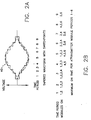
- the waveform 40 of Fig. 2A contains nine periods, wherein each period has a different amplitude.
- the waveform 40 can be produced through the selective activation of six amplifier modules.
- Fig 2B shows an activation schedule which lists the amplifier modules that are selectively activated during a given period.
- the activation schedule illustrates that the number of selected modules will gradually increase from the beginning of the waveform (Time Period 1) to the center of the wave (Time Period 5). Then the numbers of selected modules may gradually be decreased from the point of highest amplitude (Time Period 5) at the center of the wave, to the end of the wave (Time Period 9), where the amplitude again falls off.
- the number of modules and the sequence of operation are selectable to achieve the desired level of transmitted power.
- the combiner 68 of Fig. 5 achieves low loss combining using a controlling means 78 to control RF switching logic of the combiner 68 and to adjust the phase shifters 75, 76 of each coupler section, thereby avoiding loss in the termination resistors (not shown).
- the controlling means 78 is similar to the controllers previously described. Depending on the group of amplifier modules which is selected, the controlling means 78 dictates the behavior of the switching logic and the phase shifters 75, 76. In this embodiment, when all amplifiers are selected, the phase shifters 75, 76 are set to zero and the combiner 68 performs as a classical combiner wherein the signals from all active modules are combined in phase.
- the associated switch leading to the corresponding coupler section is placed in the closed position.
- the first switch 71 associated with the first amplifier module 22 is closed. This allows the amplified signal from amplifier module 22 to flow into the first coupler section 70.
- the combiner 68 will function as a classical combiner, that is the associated phase shifters 75, 76 in each coupler section 70, 80, 90 are set to zero and the two signals entering each coupler section will be combined in phase. In this case, when all the amplifier modules are selected, the signal from the first amplifier module 22 and the second amplifier module 24 will be combined in the first coupler section 70.
- the combined signal from the first coupler section 70 will then travel to the input 81 of the second coupler section 80, where it will be combined with the signal from the third amplifier module 26.
- This sequence continues in the third coupler section 90, where the combined signal from the second coupler section 80 is combined with the signal from the fourth amplifier module 28.
- the final composite signal can then be transmitted.
- the controlling means 78 causes the associated phase shifters 75, 76 in the corresponding coupler section to readjust the phase of the signal traveling through that section. In this way output power will not be lost because of the unbalanced inputs created as a result of the deactivation.
- the amplifier module 100 contains input and output controls made from PIN diodes.
- the amplifier module 100 includes an RF amplifier 102 whose output is coupled to a circulator 104.
- the circulator 104 is coupled to impedance element 106 which provides a dummy load.
- a first PIN diode 110 has its anode coupled to the input of the amplifier module 100 and a second PIN diode 120 has its cathode coupled to the output of the circulator 104, which is also the output of the amplifier module 100.
- the PIN diodes and amplifier 102 are coupled to a controller 122.
- Phase, amplitude, and spectrum stabilization is accomplished utilizing the PIN diodes 110, 120 as input and output controls.
- the amplifier 102 is activated by the controller 122.
- the first PIN diode 110 which acts as an input switch is forward biased by the controller 122 to impress signal power (from a source not shown) on the amplifier module 100.
- the amplifier 102 will then begin to output an amplified signal.
- the second PIN diode 120 which acts as an output switch, must be reverse biased to reflect the amplified signal back through the circulator 104.
- the circulator 104 circulates the signal so that the reflected power is dissipated in the impedance element 106 during phase stabilization.
Landscapes
- Engineering & Computer Science (AREA)
- Radar, Positioning & Navigation (AREA)
- Remote Sensing (AREA)
- Computer Networks & Wireless Communication (AREA)
- Physics & Mathematics (AREA)
- General Physics & Mathematics (AREA)
- Power Engineering (AREA)
- Amplifiers (AREA)
- Radar Systems Or Details Thereof (AREA)
- Microwave Amplifiers (AREA)
Applications Claiming Priority (2)
| Application Number | Priority Date | Filing Date | Title |
|---|---|---|---|
| US08/055,198 US5325099A (en) | 1993-04-28 | 1993-04-28 | Modular solid-state radar transmitter apparatus and method for producing variable waveforms |
| US55198 | 1993-04-28 |
Publications (3)
| Publication Number | Publication Date |
|---|---|
| EP0622638A2 true EP0622638A2 (de) | 1994-11-02 |
| EP0622638A3 EP0622638A3 (de) | 1994-11-30 |
| EP0622638B1 EP0622638B1 (de) | 1999-11-24 |
Family
ID=21996295
Family Applications (1)
| Application Number | Title | Priority Date | Filing Date |
|---|---|---|---|
| EP94106563A Expired - Lifetime EP0622638B1 (de) | 1993-04-28 | 1994-04-27 | Modularer Halbleiterradarsendevorrichtung und Verfahren zum Erzeugen von verstellbaren Wellenformen |
Country Status (4)
| Country | Link |
|---|---|
| US (1) | US5325099A (de) |
| EP (1) | EP0622638B1 (de) |
| JP (1) | JPH0795026A (de) |
| DE (1) | DE69421744T2 (de) |
Cited By (1)
| Publication number | Priority date | Publication date | Assignee | Title |
|---|---|---|---|---|
| EP0701332A1 (de) * | 1994-09-09 | 1996-03-13 | Kabushiki Kaisha Toshiba | Schaltung für variable Verstärkung und Radioapparat mit eines solche Schatung |
Families Citing this family (24)
| Publication number | Priority date | Publication date | Assignee | Title |
|---|---|---|---|---|
| US5781066A (en) * | 1996-03-11 | 1998-07-14 | The Mitre Corporation | Pulse waveform generator |
| NL1006924C2 (nl) * | 1997-09-03 | 1999-03-04 | Hollandse Signaalapparaten Bv | Radarzender. |
| FR2781100B1 (fr) * | 1998-07-10 | 2000-10-06 | Thomson Csf | Procede d'elaboration d'un signal d'emission et emetteur a cellules d'amplification pour la mise en oeuvre de ce procede |
| US6690251B2 (en) | 2001-04-11 | 2004-02-10 | Kyocera Wireless Corporation | Tunable ferro-electric filter |
| US7221243B2 (en) * | 2001-04-11 | 2007-05-22 | Kyocera Wireless Corp. | Apparatus and method for combining electrical signals |
| US7154440B2 (en) * | 2001-04-11 | 2006-12-26 | Kyocera Wireless Corp. | Phase array antenna using a constant-gain phase shifter |
| US7174147B2 (en) * | 2001-04-11 | 2007-02-06 | Kyocera Wireless Corp. | Bandpass filter with tunable resonator |
| US7394430B2 (en) * | 2001-04-11 | 2008-07-01 | Kyocera Wireless Corp. | Wireless device reconfigurable radiation desensitivity bracket systems and methods |
| US7164329B2 (en) | 2001-04-11 | 2007-01-16 | Kyocera Wireless Corp. | Tunable phase shifer with a control signal generator responsive to DC offset in a mixed signal |
| US7746292B2 (en) * | 2001-04-11 | 2010-06-29 | Kyocera Wireless Corp. | Reconfigurable radiation desensitivity bracket systems and methods |
| US7071776B2 (en) | 2001-10-22 | 2006-07-04 | Kyocera Wireless Corp. | Systems and methods for controlling output power in a communication device |
| US7180467B2 (en) * | 2002-02-12 | 2007-02-20 | Kyocera Wireless Corp. | System and method for dual-band antenna matching |
| US7184727B2 (en) * | 2002-02-12 | 2007-02-27 | Kyocera Wireless Corp. | Full-duplex antenna system and method |
| US7176845B2 (en) * | 2002-02-12 | 2007-02-13 | Kyocera Wireless Corp. | System and method for impedance matching an antenna to sub-bands in a communication band |
| US7720443B2 (en) | 2003-06-02 | 2010-05-18 | Kyocera Wireless Corp. | System and method for filtering time division multiple access telephone communications |
| US7248845B2 (en) * | 2004-07-09 | 2007-07-24 | Kyocera Wireless Corp. | Variable-loss transmitter and method of operation |
| US7548762B2 (en) * | 2005-11-30 | 2009-06-16 | Kyocera Corporation | Method for tuning a GPS antenna matching network |
| JP2007336187A (ja) * | 2006-06-14 | 2007-12-27 | Nippon Telegr & Teleph Corp <Ntt> | スイッチ機能つき増幅器 |
| KR101252052B1 (ko) * | 2011-12-15 | 2013-04-12 | 국방과학연구소 | 레이더 타이밍 신호 발생 방법 |
| CN103079334B (zh) * | 2013-01-04 | 2016-06-22 | 中国原子能科学研究院 | 回旋加速器射频谐振腔体自动锻炼系统 |
| WO2014178125A1 (ja) * | 2013-04-30 | 2014-11-06 | 古河電気工業株式会社 | レーダ装置 |
| CN106842141B (zh) * | 2017-04-14 | 2018-02-06 | 中国人民解放军武汉军械士官学校 | 一种高阶多次共轭滞后积脉内分析方法 |
| US10554233B2 (en) | 2017-08-03 | 2020-02-04 | International Business Machines Corporation | Reconfigurable radar transmitter |
| CN109375176B (zh) * | 2018-11-29 | 2023-10-27 | 四川九洲电器集团有限责任公司 | 一种发射机功放模块 |
Family Cites Families (8)
| Publication number | Priority date | Publication date | Assignee | Title |
|---|---|---|---|---|
| JPS5665505A (en) * | 1979-11-02 | 1981-06-03 | Tech Res & Dev Inst Of Japan Def Agency | Pulse radar system |
| DE3241466A1 (de) * | 1982-11-10 | 1984-05-10 | Brown, Boveri & Cie Ag, 6800 Mannheim | Verfahren und einrichtung zur steuerung eines mikrowellensenders |
| US4827267A (en) * | 1987-11-19 | 1989-05-02 | Itt Gilfillan | High availability solid state modulator for microwave cross-field amplifiers |
| US4965530A (en) * | 1989-09-26 | 1990-10-23 | General Electric Company | Parallelled amplifier with switched isolation resistors |
| US5083094A (en) * | 1990-09-28 | 1992-01-21 | Space Systems/Loral, Inc. | Selective power combiner using phase shifters |
| US5136300A (en) * | 1991-06-13 | 1992-08-04 | Westinghouse Electric Corp. | Modular solid state radar transmitter |
| US5146616A (en) * | 1991-06-27 | 1992-09-08 | Hughes Aircraft Company | Ultra wideband radar transmitter employing synthesized short pulses |
| DE4206195C1 (en) * | 1992-02-28 | 1993-04-15 | Rohde & Schwarz Gmbh & Co Kg, 8000 Muenchen, De | AC voltage video signal level measurer - has circuit adding output signals of amplifier and supplying a=d converter assigned to evaluator for control e.g. register |
-
1993
- 1993-04-28 US US08/055,198 patent/US5325099A/en not_active Expired - Lifetime
-
1994
- 1994-04-27 EP EP94106563A patent/EP0622638B1/de not_active Expired - Lifetime
- 1994-04-27 DE DE69421744T patent/DE69421744T2/de not_active Expired - Fee Related
- 1994-04-28 JP JP6091774A patent/JPH0795026A/ja active Pending
Cited By (2)
| Publication number | Priority date | Publication date | Assignee | Title |
|---|---|---|---|---|
| EP0701332A1 (de) * | 1994-09-09 | 1996-03-13 | Kabushiki Kaisha Toshiba | Schaltung für variable Verstärkung und Radioapparat mit eines solche Schatung |
| US5809408A (en) * | 1994-09-09 | 1998-09-15 | Kabushiki Kaisha Toshiba | Variable gain circuit and radio apparatus using the same |
Also Published As
| Publication number | Publication date |
|---|---|
| DE69421744T2 (de) | 2000-07-27 |
| JPH0795026A (ja) | 1995-04-07 |
| EP0622638B1 (de) | 1999-11-24 |
| EP0622638A3 (de) | 1994-11-30 |
| DE69421744D1 (de) | 1999-12-30 |
| US5325099A (en) | 1994-06-28 |
Similar Documents
| Publication | Publication Date | Title |
|---|---|---|
| US5325099A (en) | Modular solid-state radar transmitter apparatus and method for producing variable waveforms | |
| US5621351A (en) | Modulation amplifier for radio transmitters | |
| US5339041A (en) | High efficiency power amplifier | |
| US5017888A (en) | Broadband nonlinear drive control network for linear amplifiers arranged in several amplifier channels | |
| US5119042A (en) | Solid state power amplifier with dynamically adjusted operating point | |
| US6191735B1 (en) | Time delay apparatus using monolithic microwave integrated circuit | |
| KR100191101B1 (ko) | 고 효율을 가진 광역 가변 출력 증폭기 장치 | |
| US6320480B1 (en) | Wideband low-loss variable delay line and phase shifter | |
| EP4128530A1 (de) | Verstärkerschaltungen und verfahren zum betrieb einer verstärkerschaltung | |
| EP0956648A1 (de) | System kombinierter sender | |
| US6989788B2 (en) | Antenna array having apparatus for producing time-delayed microwave signals using selectable time delay stages | |
| EP0408323B1 (de) | Diskretes schrittweises Signalverarbeitungssystem und Verfahren, das parallel verzweigte N-Zustandsnetzwerke verwendet | |
| US20250211182A1 (en) | Amplifier peak detection | |
| WO2009009652A2 (en) | Segmented power amplifier | |
| US6646600B2 (en) | Phased array antenna with controllable amplifier bias adjustment and related methods | |
| US4056792A (en) | Wideband diode switched microwave phase shifter network | |
| US5731784A (en) | Adaptive pulse shaping implementation and method for control of solid state transmitter spectrum and time sidelobes | |
| US5243301A (en) | Microwave power amplifiers | |
| EP3440476A1 (de) | Schaltbare sende-empfang (t/r)-modul | |
| US4749950A (en) | Binary power multiplier for electromagnetic energy | |
| US5155492A (en) | Dual mode active aperture | |
| US5053720A (en) | Power amplifying circuit | |
| US7173503B1 (en) | Multibit phase shifter with active and passive phase bits, and active phase bit therefor | |
| EP0312144A2 (de) | Hochspannungsimpuls-Leistungstreiber | |
| JPH088442B2 (ja) | ステップ可変式高周波減衰器 |
Legal Events
| Date | Code | Title | Description |
|---|---|---|---|
| PUAI | Public reference made under article 153(3) epc to a published international application that has entered the european phase |
Free format text: ORIGINAL CODE: 0009012 |
|
| PUAL | Search report despatched |
Free format text: ORIGINAL CODE: 0009013 |
|
| AK | Designated contracting states |
Kind code of ref document: A2 Designated state(s): DE FR GB |
|
| AK | Designated contracting states |
Kind code of ref document: A3 Designated state(s): DE FR GB |
|
| 17P | Request for examination filed |
Effective date: 19950128 |
|
| 17Q | First examination report despatched |
Effective date: 19970218 |
|
| GRAG | Despatch of communication of intention to grant |
Free format text: ORIGINAL CODE: EPIDOS AGRA |
|
| GRAG | Despatch of communication of intention to grant |
Free format text: ORIGINAL CODE: EPIDOS AGRA |
|
| GRAH | Despatch of communication of intention to grant a patent |
Free format text: ORIGINAL CODE: EPIDOS IGRA |
|
| GRAH | Despatch of communication of intention to grant a patent |
Free format text: ORIGINAL CODE: EPIDOS IGRA |
|
| RAP1 | Party data changed (applicant data changed or rights of an application transferred) |
Owner name: ITT MANUFACTURING ENTERPRISES, INC. |
|
| GRAA | (expected) grant |
Free format text: ORIGINAL CODE: 0009210 |
|
| AK | Designated contracting states |
Kind code of ref document: B1 Designated state(s): DE FR GB |
|
| REF | Corresponds to: |
Ref document number: 69421744 Country of ref document: DE Date of ref document: 19991230 |
|
| ET | Fr: translation filed | ||
| PLBE | No opposition filed within time limit |
Free format text: ORIGINAL CODE: 0009261 |
|
| STAA | Information on the status of an ep patent application or granted ep patent |
Free format text: STATUS: NO OPPOSITION FILED WITHIN TIME LIMIT |
|
| 26N | No opposition filed | ||
| PGFP | Annual fee paid to national office [announced via postgrant information from national office to epo] |
Ref country code: FR Payment date: 20010330 Year of fee payment: 8 |
|
| PGFP | Annual fee paid to national office [announced via postgrant information from national office to epo] |
Ref country code: DE Payment date: 20010402 Year of fee payment: 8 |
|
| PGFP | Annual fee paid to national office [announced via postgrant information from national office to epo] |
Ref country code: GB Payment date: 20010403 Year of fee payment: 8 |
|
| REG | Reference to a national code |
Ref country code: GB Ref legal event code: IF02 |
|
| PG25 | Lapsed in a contracting state [announced via postgrant information from national office to epo] |
Ref country code: GB Free format text: LAPSE BECAUSE OF NON-PAYMENT OF DUE FEES Effective date: 20020427 |
|
| PG25 | Lapsed in a contracting state [announced via postgrant information from national office to epo] |
Ref country code: DE Free format text: LAPSE BECAUSE OF NON-PAYMENT OF DUE FEES Effective date: 20021101 |
|
| GBPC | Gb: european patent ceased through non-payment of renewal fee |
Effective date: 20020427 |
|
| PG25 | Lapsed in a contracting state [announced via postgrant information from national office to epo] |
Ref country code: FR Free format text: LAPSE BECAUSE OF NON-PAYMENT OF DUE FEES Effective date: 20021231 |
|
| REG | Reference to a national code |
Ref country code: FR Ref legal event code: ST |