EP0701332A1 - Schaltung für variable Verstärkung und Radioapparat mit eines solche Schatung - Google Patents
Schaltung für variable Verstärkung und Radioapparat mit eines solche Schatung Download PDFInfo
- Publication number
- EP0701332A1 EP0701332A1 EP95114241A EP95114241A EP0701332A1 EP 0701332 A1 EP0701332 A1 EP 0701332A1 EP 95114241 A EP95114241 A EP 95114241A EP 95114241 A EP95114241 A EP 95114241A EP 0701332 A1 EP0701332 A1 EP 0701332A1
- Authority
- EP
- European Patent Office
- Prior art keywords
- gain
- input
- output
- stages
- impedance values
- Prior art date
- Legal status (The legal status is an assumption and is not a legal conclusion. Google has not performed a legal analysis and makes no representation as to the accuracy of the status listed.)
- Granted
Links
Images


Classifications
-
- H—ELECTRICITY
- H03—ELECTRONIC CIRCUITRY
- H03F—AMPLIFIERS
- H03F3/00—Amplifiers with only discharge tubes or only semiconductor devices as amplifying elements
- H03F3/72—Gated amplifiers, i.e. amplifiers which are rendered operative or inoperative by means of a control signal
-
- H—ELECTRICITY
- H03—ELECTRONIC CIRCUITRY
- H03F—AMPLIFIERS
- H03F3/00—Amplifiers with only discharge tubes or only semiconductor devices as amplifying elements
- H03F3/20—Power amplifiers, e.g. Class B amplifiers, Class C amplifiers
- H03F3/21—Power amplifiers, e.g. Class B amplifiers, Class C amplifiers with semiconductor devices only
- H03F3/211—Power amplifiers, e.g. Class B amplifiers, Class C amplifiers with semiconductor devices only using a combination of several amplifiers
-
- H—ELECTRICITY
- H03—ELECTRONIC CIRCUITRY
- H03G—CONTROL OF AMPLIFICATION
- H03G1/00—Details of arrangements for controlling amplification
- H03G1/0005—Circuits characterised by the type of controlling devices operated by a controlling current or voltage signal
- H03G1/0088—Circuits characterised by the type of controlling devices operated by a controlling current or voltage signal using discontinuously variable devices, e.g. switch-operated
-
- H—ELECTRICITY
- H03—ELECTRONIC CIRCUITRY
- H03H—IMPEDANCE NETWORKS, e.g. RESONANT CIRCUITS; RESONATORS
- H03H11/00—Networks using active elements
- H03H11/02—Multiple-port networks
- H03H11/28—Impedance matching networks
-
- H—ELECTRICITY
- H03—ELECTRONIC CIRCUITRY
- H03F—AMPLIFIERS
- H03F2200/00—Indexing scheme relating to amplifiers
- H03F2200/372—Noise reduction and elimination in amplifier
-
- H—ELECTRICITY
- H03—ELECTRONIC CIRCUITRY
- H03F—AMPLIFIERS
- H03F2203/00—Indexing scheme relating to amplifiers with only discharge tubes or only semiconductor devices as amplifying elements covered by H03F3/00
- H03F2203/72—Indexing scheme relating to gated amplifiers, i.e. amplifiers which are rendered operative or inoperative by means of a control signal
- H03F2203/7236—Indexing scheme relating to gated amplifiers, i.e. amplifiers which are rendered operative or inoperative by means of a control signal the gated amplifier being switched on or off by putting into parallel or not, by choosing between amplifiers by (a ) switch(es)
-
- H—ELECTRICITY
- H03—ELECTRONIC CIRCUITRY
- H03F—AMPLIFIERS
- H03F2203/00—Indexing scheme relating to amplifiers with only discharge tubes or only semiconductor devices as amplifying elements covered by H03F3/00
- H03F2203/72—Indexing scheme relating to gated amplifiers, i.e. amplifiers which are rendered operative or inoperative by means of a control signal
- H03F2203/7239—Indexing scheme relating to gated amplifiers, i.e. amplifiers which are rendered operative or inoperative by means of a control signal the gated amplifier being switched on or off by putting into parallel or not, by choosing between amplifiers and shunting lines by one or more switch(es)
Definitions
- the present invention relates to a variable gain circuit for switching a plurality of gains and a radio apparatus using such the variable gain circuit.
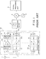
- the receiver comprises, for example, an antenna 1 for inputting a receiving signal externally transmitted, a conventional amplifier 10 for amplifying the receiving signal, a bandpass filter 2 for passing through a predetermined frequency band of the receiving signal, a frequency converter 3 for converting a frequency of the receiving signal, a local oscillator 4 for outputting a local oscillating signal, and a signal processing unit for processing a frequency converted signal.
- the level of a signal inputted from the antenna 1 diversely changes.
- gain of the amplifier 10 is not variable, distortion may take place with respect to an excessive input signal, and/or noise characteristic may become poor with respect to a very small input signal. Accordingly, it is desirable that the amplifier has variable gain so as to make attenuation with respect to an excessive input signal, and to make amplification with respect to a very small input signal.
- the amplifier 10 comprises an input terminal, first through n-th amplifier stages 12a-12n connected in parallel with one another and an output terminal 16.
- Each amplifier stage 12 comprises an input side matching circuit 13, a gain stage 14, and an output side matching circuit 15. Accordingly, respective stages are matched with an input side and output side by the matching circuits 13 and 15 to finally supply the optimum receiving signal for the signal processing unit 5.
- the antenna 1 and/or filter 2, etc. are generally disposed before and after the amplifier 10. Since these parts (circuit components) are designed on the basis of a predetermined characteristic impedance Z0 (generally, 50 ohms, and hereinafter the characteristic impedance is assumed to be 50 ohms), if the input impedance or the output impedance of the amplifier is not set to 50 ohms, antenna and/or filter disposed before and after the amplifier do not exhibit desired performance. However, since generally the input/output impedance of the amplifier itself is not in correspondence with 50 ohms, matching circuits 13 and 15 as shown in FIG. 2 are used to convert (change) the input impedance or the output impedance of the amplifier into 50 ohms.
- a predetermined characteristic impedance Z0 generally, 50 ohms, and hereinafter the characteristic impedance is assumed to be 50 ohms
- a typical matching circuit serves to convert a certain impedance into a desired impedance at a predetermined frequency. Accordingly, if frequency changes, or input impedance or output impedance of the amplifier itself changes, it is difficult to maintain matching.
- an electronic circuit for carrying out switching between plural gains is of a structure in which switching between gain stages is made by switches, or is of a structure in which respective gain stages are connected in parallel as shown in FIG. 1.
- switches 17 and 18 are connected before the matching circuit 13 and after the matching circuit 15, respectively.
- switches are not integrated within IC
- switches of externally attached parts are used.
- characteristics of respective gain stages fluctuate without conducting tracking (following) with respect to variations (unevenness) of the process.
- an object of this invention is to realize, by cheap bipolar process, without use of switch, gain switching means adapted so that input and output impedance values of the amplifier do not change even if what gain stage is selected, and that it is thus sufficient to provide matching circuits respectively on the input side and on the output side.
- a variable gain circuit is characterized in that, in gain stages connected in parallel, input impedance values of circuits nearest to the input side and output impedance values of circuits nearest to the output side are caused to be substantially the same at all gain stages, thereby permitting input and output impedance values to be substantially constant even when what gain stage is selected.
- variable gain circuit of this invention is adapted so that predetermined signal amplification factors are determined in accordance with amplification factors of the amplifying sections of plural gain stage blocks to select any one of respective gain stage blocks, thereby making it possible to obtain desired amplification factor.
- the input impedance and the output impedance of the entirety of the variable gain stage are always substantially constant (fixed) even if which gain stage is selected, i.e., irrespective of the gain stage selected. For this reason, it is unnecessary to individually provide different matching circuits at respective gain stages.
- one matching circuit is used as the entirety of the variable gain circuit, it is possible to match with a desired impedance even if which gain stage block is selected.
- the total number of matching circuits which generally occupy large area within the Integrated Circuit (IC) can be decreased.
- the chip area can be reduced as a whole.
- gain switching circuit can be put into practice even with relatively cheap process such as typical bipolar process.
- variable gain circuit having a plurality of gain stages, it becomes easy to take matching with external circuits connected to the input side and the output side, and the number of matching circuits can be reduced.
- variable gain circuit can be realized even by cheap process such as typical bipolar process.
- variable gain circuit and a radio apparatus using the same according to preferred embodiments the present invention in reference with the attached drawings.
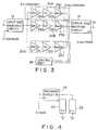
- Reference numerals 20A, 20B, ..., and 20C denote plural different gain stage blocks.
- input sections 21a, 21b, ..., and 21n, amplifying sections 22a(A1), 22b(A2), ..., and 22n(An), and output sections 23a, 23b, ..., and 23n, etc. are included.
- plural gain stage blocks are connected in a parallel fashion to thereby constitute a variable gain stage as a whole, and a matching circuit 13 of the input side and a matching circuit 14 of the output side are respectively connected before and after the variable gain stage.
- an input circuit section is constituted so that input impedance values of the circuit portions (input sections 21a, 21b, ..., and 21n of the gain stage blocks 20A-20N) nearest to the signal input terminal 11 included in the individual gain stage blocks 20A, 20B, ..., and 20N are substantially equal to each other
- an output circuit section is constituted so that output impedance values of the circuit portions (output sections 23a, 23b, ..., and 23n of the gain stage blocks 20A-20N) nearest to the signal output terminal 12 are substantially equal to one another.
- the input impedance of the entirety of the variable gain stage is affected to the maximum degree by input impedance values of the circuits nearest to the signal input terminal, i.e., the circuits of the input sections of respective gain stages, and the output impedance of the entirety of the variable gain stages is affected to the maximum degree by output impedance values of the circuit nearest to the signal output terminal, i.e. the circuits of the output sections of respective gain stages.
- input impedance values and output impedance values, etc. of the amplifying section circuits provided between the input sections and the output sections of the gain stage blocks have less influence on the input impedance and the output impedance of the entirety of the variable gain stage.
- the gain swi ching circuit of this invention is adapted so that predetermined signal amplification factors are determined in dependency upon amplification factors of the amplifying sections of plural gain stage blocks to select any one of respective gain stage blocks, thereby ma. ing it possible to obtain a desired amplification factor.
- the input impedance and the output impedance of the entirety of the variable gain stage are always substantially constant (fixed) even if which gain stage is selected, i.e., irrespective of the gain stage selected. For this reason, it is unnecessary to individually provide different matching circuits at respective gain stages.
- one matching circuit is used as the entirety of the gain switching circuit, it is possible to match with a desired impedance. even if which gain stage block is selected.
- the variable gain circuit can be put into practice even with relatively cheap process such as typical bipolar process.
- FIG. 3 The fundamental configuration of the variable gain circuit of this invention is shown in FIG. 3. Respective input impedance values of circuits nearest to the input side (input sections 21a, 21b, ..., and 21n) and output impedance values of circuits nearest to the output side (output sections 23a, 23b, ..., and 23n) of respective gain stage blocks 20A, 20B, ..., and 20N are caused to be substantially the same at all gain stages, wherein a control unit 24 carries out selection of gain stage block in accordance with a desired gain.
- a matching circuit 25 is connected to a circuit comprising a circuit 26 of input impedance Zin and a circuit 27 of input impedance Zin' connected in parallel.
- this circuit arrangement has an input impedance Zm such that the voltage standing wave ratio (VSWR) at the input terminal is expressed as "VSWR ⁇ 3", since power reflected at the input terminal is less than one half, Zin and Zin' are considered to be substantially the same impedance.
- the control unit 24 is caused to be operative so that only the gain stage 20A is turned ON and other gain stages 20B-20N are all turned OFF.
- the gain of the circuit of FIG. 3 is expressed as Ain + A1 + Aout [dB].
- the input impedance and the output impedance of this circuit are substantially determined by the input impedance values of circuits nearest to the input side and the output impedance values of circuits nearest to the output side of respective gain stages. In the case of the circuit of FIG. 3, even if which gain stage is selected, only one gain stage selected of the circuits nearest to the input side of respective gain stages is in ON state, and circuits of other gain stages are all in OFF state.
- Input impedance of the circuit of FIG. 6 is equal to a value when input impedance (Zon) of one input side circuit in ON state denoted by reference numeral 28 and input impedance (Zoff) of (n-1) input side circuits in OFF state denoted by reference numeral 29 are connected in parallel. Since this state is the same even if which gain stage is selected, i.e., irrespective of gain stage selected, the input impedance of the circuit of FIG. 3 is fixed (constant) even if which gain stage is selected.
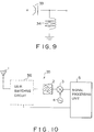
- Individual circuits at respective gain stages of FIG. 3 may be, e.g., an emitter-grounded amplifier 30 as shown in FIG. 7, or may be an attenuator 31 in which resistance elements 32a-32c are connected in ⁇ form as shown in FIG. 8.
- the circuit form, the magnitude of gain, and magnitude of quantity of attenuation are arbitrary. Generally, dimensions of these circuits are about 100 ⁇ m at the best.
- the inductor 34 and capacitor 33 respectively have great area more than several hundreds ⁇ m and 100 ⁇ m. Accordingly, in the case of the circuit of FIG. 3, since circuits less than 100 ⁇ m are only provided in respective stages so that the number of matching circuits which occupy large area can be reduced, the chip area can be reduced.
- FIG. 10 shows an example where the circuit of FIG. 3 is used as a radio receiver 35.
- a receiving signal inputted from an antenna section 1 is converted into a base band signal by a frequency converter 3 through a band-pass filter 2.
- the base band signal thus obtained is converted into speech/picture data, etc. by a signal processing unit 5.
- the signal processing unit 5 judges magnitude of signal amplitude. In the case where the signal processing unit 5 detects changes (fluctuation) of the level of a receiving signal, it outputs a control signal to control unit (not shown) of a variable gain circuit 36 in the manner of having the above-mentioned configuration or the like.
- the signal processing unit 5 When the radio receiver receives, e.g., a signal of amplitude value of a predetermined level or more, the signal processing unit 5 outputs a control signal to allow quantity of attenuation of signal amplitude to be large. In the case where the signal processing unit 5 cannot detect a signal of amplitude value of a predetermined level, it outputs a control signal to allow attenuation quantity of signal amplitude to be small.
- antenna and/or filter disposed before and after the gain switching circuit indicate satisfactory characteristic, and there results no unnecessary reflection taking place in the case where those elements do not match with 50 ohms.
- the circuit shown in FIG. 11 is of a structure comprising gain stage blocks 20A, 20B, ..., and 20N connected in parallel so that output impedance values of circuits nearest to the output side (output sections 23a, 23b, ..., and 23n) of respective gain stage blocks 20A, 20B, ..., and 20N are caused to be equal to each other at all the gain stages.
- output impedance of the circuit of FIG. 11 In order to select gain stage 20A in this circuit, only the gain stage 20A is caused to be turned ON, and other all gain stages are caused to be turned OFF. Thus, the output impedance of the circuit of FIG.
- the input impedance becomes constant even if which gain stage 20A, 20B, ..., or 20N is selected.
- circuits nearest to the input side (input sections 21a, 21b, ..., and 21n) of respective gain stage blocks 20A, 20B, ..., and 20N adapted so that input impedance values are equal to each other at all gain stages are used to provide a configuration comprising these circuits connected in parallel so that the input impedance becomes constant.
- circuits nearest to the input side input sections 41a, 41b, ..., and 41n
- circuits nearest to the output side output sections 43a, 43b, ..., and 43n
- input impedance values of the circuits nearest to the input side and output impedance values of the circuits nearest to the output side vary (fluctuate) while carrying out tracking with respect to variations of the process. For this reason, irrespective of gain stage selected, the input impedance and the output impedance of the entirety of the circuit shown in FIG. 13 become constant.
- Numerals 42a, 42b, ..., 42n denote amplifying sections in the gain stage blocks 40A, 40B, ..., 40N.
- circuits nearest to the input side (input sections 44a, 44b, 44c, ..., and 44n) and circuits nearest to the output side (46a, 46b, 46c, ..., 46n) of all gain stage blocks (45A, 45B, 45C, ..., and 45N) are caused to have the same circuit configuration and the same circuit constants, the portions except for the above are respectively constituted by using the same circuits, and differences between gains prescribing amplification factors of respective gain stages are determined by varying the number of stages of circuits connected. With respect to the input impedance and the output impedance of this circuit, similarly to the case of the circuit of FIG. 13, they are constant even if which gain stage is selected. Moreover, in FIG.
- gain difference between gain stage 45A and gain stage 45B becomes equal to magnitude A of unit gain of unit gain block 47a, ..., or 4mn, and gain difference between gain stage 45B and gain stage 45C also becomes equal to A .
- gain differences between respective gains stages become equal to A .
- the final gain stage block 45N includes intermediate gain section 47n through 4mn at m stages.
- the circuit of FIG. 15 is adapted so that circuits nearest to the input side (51a, 51b, 51c, ..., and 51n) and circuits nearest to the output side (53a, 53b, 53c, ..., and 53n) of all gain stage blocks 50A, 50B, 50C, ..., and 50N are caused to have the same circuit configuration and the same circuit constants, portions of amplifying sections 52a, 52b, ..., and 52n are respectively constituted by using circuits of the same configuration, and difference of gains between respective gain stages are determined by prescribing a way of giving bias current delivered to the circuits of the amplifying sections. That is, the gain stage blocks 50A-50N respectively comprise current sources 54a, 54b, ..., 54n.
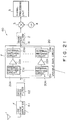
- FIG. 16 is a circuit diagram showing a variable gain circuit according to a first concrete example including a matching circuit on an input terminal side.
- the variable gain circuit of the first example corresponds to the circuit shown in FIG. 12, and comprises an input side matching circuit 13, and a plurality of gain stage blocks 20A through 20N.
- the gain stage block 20A comprises an input amplifier section 21a, capacitors Ca1 and Ca2, and an amplifier section 22a
- the gain stage block 20N comprises an inut section 21n, capacitors Cn1 and Cn2, and an attenuator section 22n.
- the matching circuit 13 is comprised of an LC circuit.
- the amplifier stages 21a through 21n have the same input impedance value viewed from the input terminal 11. Since the circuit 22a is the amplifier and the circuit 22n is the attenuator, both the cirucits generally have different output impedance value, repectively. Accordingly, in this example, an inpedance matching is performed only on the input side in accordance with the present invention.
- FIG. 17 is a circuit diagram showing a variable gain circuit according to a second concrete example including a matching circuit on an output side.
- the variable gain circuit of the second example corresponds to the circuit shown in FIG. 11, and comprises a plurality of gain stage blocks 20A through 20N connected in parallel with one another, and an output side matching circuit 14.
- the first gain stage block 20A comprises an input stage 21a, amplifier stage 22a and output stage 23a
- the N-th gain stage block 20N comprises a section 21n, 22n and 23n.
- the matching circuit 14 is also comprised of an LC circuit.
- FIG. 18 is a circuit diagram showing a variable gain cirucit according to a third concrete example including matching circuits on both input and output sides.
- the variable gain circuit of the third example corresponds to the circuit shown in FIG. 3, and comprises matching circuits 13 and 14, and a plurality of first through N-th gain stage blocks 20A through 20N.
- the first gain stage block 20A comprises an input stage 21a, amplifier stage 22a and output stage 23a, and capacitors Ca1 and Ca2.
- the N-th gain stage block 20N comprises an input stage 21n, attenuator stage 22n and output stage 23n, and capacitors Cn1 and Cn2.
- the matching circuits 13 and 14 are respectively comprised of an LC circuit.
- FIG. 19 is an equvalent circuit diagram of the gain circuit shown in FIG. 17.
- the gain stages are comprised of the first and second gain stages which respectively have a dynamic range as follows.
- the lower limit of the dynamic range of the amplifier is determined by a noise characteristic
- the upper limit of the dynamic range is determined by a distortion characteristic when the amplifier includes active elements (transistors).
- the gain circuit is comprised of an active element such as the amplifier stage block 20A shown in FIG. 17, the block 20A has a dynamic range between -100 dBm and -25 dBm without noise and distortion characteristics of the amplifier.
- the amplifier 23n shown in FIG. 19 has the dynamic range from -100 dBm to -25 dBm as a single body.
- the attenuator 20N when the signal is attenuated with 30 dB by the attenuator stage block 20N having a ⁇ type resistors, as shown in FIG. 19, the attenuator 20N attenuates the signal level with 20 dB from an input signal having -100 dBm which is originally sufficient to an amplifier single body, so that the signal level is buried in the noise level, thereby disabling the receiver to receive the input signal. Accordingly, when the attenuator is provided at the initial stage such as the circuit FIG. 17 (FIG. 19), the dynamic range becomes narrower with an attenuated component, that is, 20 dB.
- the attenuated component by the initial stage attenuator when the large amount of the signal power is supplied, it is advantageous with the attenuated component by the initial stage attenuator.
- the signal having the level of -25 dBm which is a limit value receivable to the amplifier single body without distortion is supplied, it is possible to receive the signal with a predetermined margine because the attenuator attenuates the signal level with 20 dB. Accordingly, the upper limit of the dynamic range seems to be broadened with an attenuated amount of te attenuator. This principle can be shown in FIG. 20.
- the dynamic range is required for the signal reception from -100 dBm to +5 dBm.
- the attenuation amount is necessary for about 30 dB.
- the amplifier block and attenuator block respectively have the different distortion and noise characteristics and attenuator block has an extreme distortion characteristic, the upper limit of the dynamic range is improved. Accordingly, 20 dB may be attenuated in actual to obtain the sufficient signal reception.
- the stage number of the variable gain stage blocks is generally two stages, the difference of the individual stages may be sufficient to be about 30 dB.
- proper margines are provided between the adjacent two blocks, respectively.
- FIG. 21 there is described a radio apparatus according to a preferred embodiment of the present invention with reference to FIG. 21.
- the duplicated description will be omitted with respect to components having the same numerals in FIG. 1.
- the radio apparatus 60 comprises an antenna 1, a low noise amplifier 61, band-pass filter, variable gain circuit 20, band-pass filter 2, frequency converter 3, local oscillator 4,and signal processing unit 5. It is possible for such a constitution to obtain the optimum reception signal by changing over the optimum gain by the variable gain circuit.
- the low noise amplifier 61 and band-pass filter 62 may constitute a reception circuit for receiving the input signal throughthe antenna 1.
Landscapes
- Engineering & Computer Science (AREA)
- Power Engineering (AREA)
- Amplifiers (AREA)
- Input Circuits Of Receivers And Coupling Of Receivers And Audio Equipment (AREA)
- Control Of Amplification And Gain Control (AREA)
Applications Claiming Priority (3)
| Application Number | Priority Date | Filing Date | Title |
|---|---|---|---|
| JP6215612A JPH0879116A (ja) | 1994-09-09 | 1994-09-09 | 利得切り替え回路及びこれを用いた無線装置 |
| JP215612/94 | 1994-09-09 | ||
| JP21561294 | 1994-09-09 |
Publications (2)
| Publication Number | Publication Date |
|---|---|
| EP0701332A1 true EP0701332A1 (de) | 1996-03-13 |
| EP0701332B1 EP0701332B1 (de) | 2003-07-16 |
Family
ID=16675306
Family Applications (1)
| Application Number | Title | Priority Date | Filing Date |
|---|---|---|---|
| EP95114241A Expired - Lifetime EP0701332B1 (de) | 1994-09-09 | 1995-09-11 | Schaltung für variable Verstärkung und Radioapparat mit einer solchen Schaltung |
Country Status (4)
| Country | Link |
|---|---|
| US (1) | US5809408A (de) |
| EP (1) | EP0701332B1 (de) |
| JP (1) | JPH0879116A (de) |
| DE (1) | DE69531273T2 (de) |
Cited By (5)
| Publication number | Priority date | Publication date | Assignee | Title |
|---|---|---|---|---|
| EP0998033A4 (de) * | 1998-05-14 | 2004-07-07 | Mitsubishi Electric Corp | Halbleiterschaltung |
| EP1708361A2 (de) * | 2005-03-29 | 2006-10-04 | Integrant Technologies Inc. | Rauscharmer Verstärker und Differenzverstärker mit variablem Verstärkungsmodus |
| EP2073383A1 (de) | 2007-12-19 | 2009-06-24 | Sequans Communications | Verstärkeranordnung |
| DE19755164B4 (de) * | 1996-12-18 | 2012-01-05 | Siemens Ag | Leistungsstufe eines Verstärkers/Senders |
| CN111162809A (zh) * | 2019-12-13 | 2020-05-15 | 西安易朴通讯技术有限公司 | 无线接收机及无线设备 |
Families Citing this family (13)
| Publication number | Priority date | Publication date | Assignee | Title |
|---|---|---|---|---|
| JP3180682B2 (ja) * | 1996-09-19 | 2001-06-25 | 日本電気株式会社 | 受信機 |
| US6121840A (en) * | 1996-12-24 | 2000-09-19 | Murata Manufacturing Co., Ltd. | High-frequency amplifier |
| US5805006A (en) * | 1997-04-28 | 1998-09-08 | Marvell Technology Group, Ltd. | Controllable integrator |
| US6417730B1 (en) | 2000-11-29 | 2002-07-09 | Harris Corporation | Automatic gain control system and related method |
| KR100651159B1 (ko) * | 2002-06-01 | 2006-11-29 | 김송강 | 고효율 전력 증폭기 |
| AU2002952531A0 (en) * | 2002-11-06 | 2002-11-21 | Telstra Corporation Limited | A transmit antenna |
| US7209727B2 (en) * | 2003-06-12 | 2007-04-24 | Broadcom Corporation | Integrated circuit radio front-end architecture and applications thereof |
| US7053717B2 (en) * | 2003-10-14 | 2006-05-30 | M/A-Com, Inc. | Method and apparatus for realizing a low noise amplifier |
| JP2005184409A (ja) * | 2003-12-19 | 2005-07-07 | Renesas Technology Corp | 通信用半導体集積回路およびそれを搭載した電子部品 |
| US7313416B1 (en) * | 2004-09-01 | 2007-12-25 | Rockwell Collins, Inc. | Scalable power amplifier |
| US7526256B2 (en) * | 2005-05-25 | 2009-04-28 | Broadcom Corporation | Transformer-based multi-band RF front-end architecture |
| US8634766B2 (en) | 2010-02-16 | 2014-01-21 | Andrew Llc | Gain measurement and monitoring for wireless communication systems |
| JP7740756B1 (ja) * | 2024-07-23 | 2025-09-17 | 有限会社ファインチューン | アナログ乗算器 |
Citations (4)
| Publication number | Priority date | Publication date | Assignee | Title |
|---|---|---|---|---|
| GB2071945A (en) * | 1980-01-03 | 1981-09-23 | Weinholt D | Apparatus for controlling the amplitude of an analog signal |
| JPH01204477A (ja) * | 1988-02-09 | 1989-08-17 | Nec Corp | 電界効果型超高周波半導体装置 |
| EP0622638A2 (de) * | 1993-04-28 | 1994-11-02 | International Standard Electric Corporation | Modularer Halbleiterradarsendevorrichtung und Verfahren zum Erzeugen von verstellbaren Wellenformen |
| EP0658977A1 (de) * | 1993-12-17 | 1995-06-21 | Thomson-Csf Semiconducteurs Specifiques | Verstärker mit einstellbarer Verstärkung |
Family Cites Families (6)
| Publication number | Priority date | Publication date | Assignee | Title |
|---|---|---|---|---|
| US3654566A (en) * | 1969-11-06 | 1972-04-04 | Gmbh Fernseh | Video cross bar distributor |
| US4598252A (en) * | 1984-07-06 | 1986-07-01 | Itt Corporation | Variable gain power amplifier |
| CA1266707A (en) * | 1985-12-16 | 1990-03-13 | Steve S. Yang | Method of calibrating and equalizing a multi-channel automatic gain control amplifier |
| FR2608862A1 (fr) * | 1986-12-19 | 1988-06-24 | Radiotechnique Ind & Comm | Commutateur electronique a tres haute frequence |
| NL8701641A (nl) * | 1987-07-13 | 1989-02-01 | Philips Nv | Tv-hf ingangsschakeling. |
| US5233634A (en) * | 1989-10-18 | 1993-08-03 | Nokia Mobile Phones Ltd. | Automatic gain control circuit in a radio telephone receiver |
-
1994
- 1994-09-09 JP JP6215612A patent/JPH0879116A/ja active Pending
-
1995
- 1995-09-08 US US08/525,061 patent/US5809408A/en not_active Expired - Lifetime
- 1995-09-11 DE DE69531273T patent/DE69531273T2/de not_active Expired - Lifetime
- 1995-09-11 EP EP95114241A patent/EP0701332B1/de not_active Expired - Lifetime
Patent Citations (4)
| Publication number | Priority date | Publication date | Assignee | Title |
|---|---|---|---|---|
| GB2071945A (en) * | 1980-01-03 | 1981-09-23 | Weinholt D | Apparatus for controlling the amplitude of an analog signal |
| JPH01204477A (ja) * | 1988-02-09 | 1989-08-17 | Nec Corp | 電界効果型超高周波半導体装置 |
| EP0622638A2 (de) * | 1993-04-28 | 1994-11-02 | International Standard Electric Corporation | Modularer Halbleiterradarsendevorrichtung und Verfahren zum Erzeugen von verstellbaren Wellenformen |
| EP0658977A1 (de) * | 1993-12-17 | 1995-06-21 | Thomson-Csf Semiconducteurs Specifiques | Verstärker mit einstellbarer Verstärkung |
Non-Patent Citations (1)
| Title |
|---|
| PATENT ABSTRACTS OF JAPAN vol. 013, no. 507 (E - 845) 14 November 1989 (1989-11-14) * |
Cited By (7)
| Publication number | Priority date | Publication date | Assignee | Title |
|---|---|---|---|---|
| DE19755164B4 (de) * | 1996-12-18 | 2012-01-05 | Siemens Ag | Leistungsstufe eines Verstärkers/Senders |
| EP0998033A4 (de) * | 1998-05-14 | 2004-07-07 | Mitsubishi Electric Corp | Halbleiterschaltung |
| EP1708361A2 (de) * | 2005-03-29 | 2006-10-04 | Integrant Technologies Inc. | Rauscharmer Verstärker und Differenzverstärker mit variablem Verstärkungsmodus |
| EP2073383A1 (de) | 2007-12-19 | 2009-06-24 | Sequans Communications | Verstärkeranordnung |
| US7994855B2 (en) | 2007-12-19 | 2011-08-09 | Sequans Communications Limited | Amplifier arrangement |
| CN111162809A (zh) * | 2019-12-13 | 2020-05-15 | 西安易朴通讯技术有限公司 | 无线接收机及无线设备 |
| CN111162809B (zh) * | 2019-12-13 | 2022-04-15 | 西安易朴通讯技术有限公司 | 无线接收机及无线设备 |
Also Published As
| Publication number | Publication date |
|---|---|
| JPH0879116A (ja) | 1996-03-22 |
| DE69531273D1 (de) | 2003-08-21 |
| DE69531273T2 (de) | 2004-05-27 |
| US5809408A (en) | 1998-09-15 |
| EP0701332B1 (de) | 2003-07-16 |
Similar Documents
| Publication | Publication Date | Title |
|---|---|---|
| US5809408A (en) | Variable gain circuit and radio apparatus using the same | |
| US5513387A (en) | Automatic gain control circuit | |
| US6181206B1 (en) | Low noise RF amplifier with programmable gain | |
| US7245890B2 (en) | High frequency variable gain amplification device, control device, high frequency variable gain frequency-conversion device, and communication device | |
| CN1110136C (zh) | 调谐带通滤波器的设备和方法 | |
| US5694085A (en) | High-power amplifier using parallel transistors | |
| CA2189712C (en) | Variable gain amplifying device | |
| JPH0211005A (ja) | 無条件に安定な超低雑音rf前置増幅器 | |
| KR19990008358A (ko) | 무선 수신기에 관한 또는 무선 수신기에 있어서의 개선 방법 | |
| US6326842B1 (en) | Variable gain amplifying apparatus which can change a gain during an operation | |
| KR950000080B1 (ko) | 적응 대역폭 증폭기, if 증폭기/검파기 및 그 신호 대 잡음비의 최적화 방법 | |
| EP0660511B1 (de) | Automatische Verstärkungsregelung in Radioempfängern | |
| US4283693A (en) | Amplitude tilt compensating apparatus | |
| US5918166A (en) | Level control circuit for portable radio communication apparatus | |
| EP1581995B1 (de) | Regelbarer hf-breitbandverstärker mit konstanter eingangsimpedanz | |
| EP0722627B1 (de) | Verbesserungen einen null-zwischenfrequenz-empfänger betreffend | |
| JPH0758563A (ja) | ステップ減衰器 | |
| KR100303311B1 (ko) | 이동통신 단말기에서 무선신호 수신 회로 및 장치 | |
| JPH03145339A (ja) | Amラジオ受信機 | |
| JPH05300039A (ja) | 受信装置 | |
| JPH0349480Y2 (de) | ||
| JP3074990B2 (ja) | 電子チューナ | |
| JPH0722975A (ja) | Amラジオ受信機 | |
| JPH033407A (ja) | 超高周波領域で利用し得る利得調整可能な増幅器 | |
| JPH0292173A (ja) | アンテナダイバーシティ方式のテレビジョン受像機 |
Legal Events
| Date | Code | Title | Description |
|---|---|---|---|
| PUAI | Public reference made under article 153(3) epc to a published international application that has entered the european phase |
Free format text: ORIGINAL CODE: 0009012 |
|
| 17P | Request for examination filed |
Effective date: 19950911 |
|
| AK | Designated contracting states |
Kind code of ref document: A1 Designated state(s): DE FR GB |
|
| 17Q | First examination report despatched |
Effective date: 20020812 |
|
| GRAH | Despatch of communication of intention to grant a patent |
Free format text: ORIGINAL CODE: EPIDOS IGRA |
|
| GRAH | Despatch of communication of intention to grant a patent |
Free format text: ORIGINAL CODE: EPIDOS IGRA |
|
| GRAA | (expected) grant |
Free format text: ORIGINAL CODE: 0009210 |
|
| AK | Designated contracting states |
Designated state(s): DE FR GB |
|
| PG25 | Lapsed in a contracting state [announced via postgrant information from national office to epo] |
Ref country code: FR Free format text: LAPSE BECAUSE OF FAILURE TO SUBMIT A TRANSLATION OF THE DESCRIPTION OR TO PAY THE FEE WITHIN THE PRESCRIBED TIME-LIMIT Effective date: 20030716 |
|
| REG | Reference to a national code |
Ref country code: GB Ref legal event code: FG4D |
|
| REF | Corresponds to: |
Ref document number: 69531273 Country of ref document: DE Date of ref document: 20030821 Kind code of ref document: P |
|
| PG25 | Lapsed in a contracting state [announced via postgrant information from national office to epo] |
Ref country code: GB Free format text: LAPSE BECAUSE OF NON-PAYMENT OF DUE FEES Effective date: 20031016 |
|
| PLBE | No opposition filed within time limit |
Free format text: ORIGINAL CODE: 0009261 |
|
| STAA | Information on the status of an ep patent application or granted ep patent |
Free format text: STATUS: NO OPPOSITION FILED WITHIN TIME LIMIT |
|
| GBPC | Gb: european patent ceased through non-payment of renewal fee |
Effective date: 20031016 |
|
| 26N | No opposition filed |
Effective date: 20040419 |
|
| EN | Fr: translation not filed | ||
| PGFP | Annual fee paid to national office [announced via postgrant information from national office to epo] |
Ref country code: DE Payment date: 20110907 Year of fee payment: 17 |
|
| REG | Reference to a national code |
Ref country code: DE Ref legal event code: R119 Ref document number: 69531273 Country of ref document: DE Effective date: 20130403 |
|
| PG25 | Lapsed in a contracting state [announced via postgrant information from national office to epo] |
Ref country code: DE Free format text: LAPSE BECAUSE OF NON-PAYMENT OF DUE FEES Effective date: 20130403 |