EP0622775B1 - Dispositif et méthode pour la génération d'horloge pour un dispositif d'affichage - Google Patents
Dispositif et méthode pour la génération d'horloge pour un dispositif d'affichage Download PDFInfo
- Publication number
- EP0622775B1 EP0622775B1 EP94106558A EP94106558A EP0622775B1 EP 0622775 B1 EP0622775 B1 EP 0622775B1 EP 94106558 A EP94106558 A EP 94106558A EP 94106558 A EP94106558 A EP 94106558A EP 0622775 B1 EP0622775 B1 EP 0622775B1
- Authority
- EP
- European Patent Office
- Prior art keywords
- signal
- display
- synchronizing signal
- dot clock
- generating
- Prior art date
- Legal status (The legal status is an assumption and is not a legal conclusion. Google has not performed a legal analysis and makes no representation as to the accuracy of the status listed.)
- Expired - Lifetime
Links
- 238000000034 method Methods 0.000 title claims description 10
- 230000008859 change Effects 0.000 claims abstract description 12
- 230000001360 synchronised effect Effects 0.000 claims description 34
- 230000004044 response Effects 0.000 claims description 7
- 238000001514 detection method Methods 0.000 claims 6
- 230000007274 generation of a signal involved in cell-cell signaling Effects 0.000 claims 2
- 230000004075 alteration Effects 0.000 claims 1
- 102100029968 Calreticulin Human genes 0.000 description 20
- 238000010586 diagram Methods 0.000 description 8
- 101100412394 Drosophila melanogaster Reg-2 gene Proteins 0.000 description 7
- 230000006835 compression Effects 0.000 description 6
- 238000007906 compression Methods 0.000 description 6
- 101001044053 Mus musculus Lithostathine-1 Proteins 0.000 description 5
- 230000015572 biosynthetic process Effects 0.000 description 5
- 238000006243 chemical reaction Methods 0.000 description 5
- 238000003786 synthesis reaction Methods 0.000 description 5
- 230000000694 effects Effects 0.000 description 3
- 230000008569 process Effects 0.000 description 3
- 238000000926 separation method Methods 0.000 description 3
- 238000009792 diffusion process Methods 0.000 description 2
- 230000006870 function Effects 0.000 description 2
- 230000010365 information processing Effects 0.000 description 2
- 238000005070 sampling Methods 0.000 description 2
- 101100326671 Homo sapiens CALR gene Proteins 0.000 description 1
- 230000005540 biological transmission Effects 0.000 description 1
- 238000010276 construction Methods 0.000 description 1
- 230000001747 exhibiting effect Effects 0.000 description 1
- 239000005262 ferroelectric liquid crystals (FLCs) Substances 0.000 description 1
- 230000020169 heat generation Effects 0.000 description 1
- 230000006872 improvement Effects 0.000 description 1
- 230000007257 malfunction Effects 0.000 description 1
- 230000006386 memory function Effects 0.000 description 1
- 238000012986 modification Methods 0.000 description 1
- 230000004048 modification Effects 0.000 description 1
- 230000002093 peripheral effect Effects 0.000 description 1
- 238000004321 preservation Methods 0.000 description 1
- 238000003672 processing method Methods 0.000 description 1
Images


Classifications
-
- G—PHYSICS
- G09—EDUCATION; CRYPTOGRAPHY; DISPLAY; ADVERTISING; SEALS
- G09G—ARRANGEMENTS OR CIRCUITS FOR CONTROL OF INDICATING DEVICES USING STATIC MEANS TO PRESENT VARIABLE INFORMATION
- G09G5/00—Control arrangements or circuits for visual indicators common to cathode-ray tube indicators and other visual indicators
- G09G5/003—Details of a display terminal, the details relating to the control arrangement of the display terminal and to the interfaces thereto
- G09G5/006—Details of the interface to the display terminal
- G09G5/008—Clock recovery
-
- G—PHYSICS
- G09—EDUCATION; CRYPTOGRAPHY; DISPLAY; ADVERTISING; SEALS
- G09G—ARRANGEMENTS OR CIRCUITS FOR CONTROL OF INDICATING DEVICES USING STATIC MEANS TO PRESENT VARIABLE INFORMATION
- G09G3/00—Control arrangements or circuits, of interest only in connection with visual indicators other than cathode-ray tubes
- G09G3/20—Control arrangements or circuits, of interest only in connection with visual indicators other than cathode-ray tubes for presentation of an assembly of a number of characters, e.g. a page, by composing the assembly by combination of individual elements arranged in a matrix no fixed position being assigned to or needed to be assigned to the individual characters or partial characters
- G09G3/34—Control arrangements or circuits, of interest only in connection with visual indicators other than cathode-ray tubes for presentation of an assembly of a number of characters, e.g. a page, by composing the assembly by combination of individual elements arranged in a matrix no fixed position being assigned to or needed to be assigned to the individual characters or partial characters by control of light from an independent source
- G09G3/36—Control arrangements or circuits, of interest only in connection with visual indicators other than cathode-ray tubes for presentation of an assembly of a number of characters, e.g. a page, by composing the assembly by combination of individual elements arranged in a matrix no fixed position being assigned to or needed to be assigned to the individual characters or partial characters by control of light from an independent source using liquid crystals
- G09G3/3611—Control of matrices with row and column drivers
- G09G3/3622—Control of matrices with row and column drivers using a passive matrix
- G09G3/3629—Control of matrices with row and column drivers using a passive matrix using liquid crystals having memory effects, e.g. ferroelectric liquid crystals
-
- G—PHYSICS
- G09—EDUCATION; CRYPTOGRAPHY; DISPLAY; ADVERTISING; SEALS
- G09G—ARRANGEMENTS OR CIRCUITS FOR CONTROL OF INDICATING DEVICES USING STATIC MEANS TO PRESENT VARIABLE INFORMATION
- G09G5/00—Control arrangements or circuits for visual indicators common to cathode-ray tube indicators and other visual indicators
- G09G5/36—Control arrangements or circuits for visual indicators common to cathode-ray tube indicators and other visual indicators characterised by the display of a graphic pattern, e.g. using an all-points-addressable [APA] memory
- G09G5/363—Graphics controllers
- G09G5/366—Graphics controllers with conversion of CRT control signals to flat panel control signals, e.g. adapting the palette memory
-
- H—ELECTRICITY
- H03—ELECTRONIC CIRCUITRY
- H03L—AUTOMATIC CONTROL, STARTING, SYNCHRONISATION OR STABILISATION OF GENERATORS OF ELECTRONIC OSCILLATIONS OR PULSES
- H03L7/00—Automatic control of frequency or phase; Synchronisation
- H03L7/06—Automatic control of frequency or phase; Synchronisation using a reference signal applied to a frequency- or phase-locked loop
- H03L7/16—Indirect frequency synthesis, i.e. generating a desired one of a number of predetermined frequencies using a frequency- or phase-locked loop
- H03L7/18—Indirect frequency synthesis, i.e. generating a desired one of a number of predetermined frequencies using a frequency- or phase-locked loop using a frequency divider or counter in the loop
-
- G—PHYSICS
- G09—EDUCATION; CRYPTOGRAPHY; DISPLAY; ADVERTISING; SEALS
- G09G—ARRANGEMENTS OR CIRCUITS FOR CONTROL OF INDICATING DEVICES USING STATIC MEANS TO PRESENT VARIABLE INFORMATION
- G09G2310/00—Command of the display device
- G09G2310/04—Partial updating of the display screen
-
- G—PHYSICS
- G09—EDUCATION; CRYPTOGRAPHY; DISPLAY; ADVERTISING; SEALS
- G09G—ARRANGEMENTS OR CIRCUITS FOR CONTROL OF INDICATING DEVICES USING STATIC MEANS TO PRESENT VARIABLE INFORMATION
- G09G3/00—Control arrangements or circuits, of interest only in connection with visual indicators other than cathode-ray tubes
- G09G3/20—Control arrangements or circuits, of interest only in connection with visual indicators other than cathode-ray tubes for presentation of an assembly of a number of characters, e.g. a page, by composing the assembly by combination of individual elements arranged in a matrix no fixed position being assigned to or needed to be assigned to the individual characters or partial characters
- G09G3/2007—Display of intermediate tones
- G09G3/2059—Display of intermediate tones using error diffusion
Definitions
- the present invention relates to display control apparatus and, in particular, to display control apparatus which performs display control by generating a multiple frequency from the frequency of a reference signal.
- oscillator circuits controlled by a phase difference signal i.e., PLL (phase locked loop) have been used.
- PLL phase locked loop
- oscillator circuits a VCO (voltage control oscillator) type oscillator for generating basic clock pulses.
- An output signal of this voltage control oscillator is divided by a predetermined division value (a preset value), and then a reference signal is compared in phase with the divided frequency to effect locking.
- the above oscillator presents the problem that only one preset value can be set, so that, when the reference signal has different frequencies, the display control apparatus constituting the PLL does not operate in a normal manner. As a result, the amount of jitter increases or the PLL itself does not lock.
- the number of values corresponds to the number of the frequencies of the reference signal.
- the invention is directed to display control in which a dot clock signal is produced in response to a synchronous signal to effect control of a video signal display.
- the synchronous signal is compared with a multiplication signal obtained from a multiplication value and the dot clock signal and the dot clock signal is generated according to the comparison result.
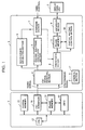
- Fig. 1 is a block diagram showing an information processing system having a display control apparatus according to a first embodiment of the present invention.
- numeral 1 indicates a display control apparatus according to the present invention.
- Numeral 2 indicates an information source for the display control apparatus 1. This information source consists, for example, of a personal computer or a work station.
- Numeral 3 indicates a display panel unit for displaying image information.
- the display panel unit 3 contains a drive circuit for driving the display panel unit, a control circuit for controlling in such a way that the display panel is operated in an optimum condition, a back light for the panel unit, a power source, etc. These circuits (not shown) are well known in the art.
- the display panel unit may, for example, use a ferroelectric liquid crystal, as the display medium.
- Numeral 4 indicates a CRT signal receiving section, which receives CRT signals (image signals and synchronous signals) output from the computer 2, and converts them into signals suitable for the subsequent processes to be conducted by processing sections in the apparatus.
- the CRT signal receiving section comprises an A/D conversion section, a PLL circuit section for generating sampling clock pulses for A/D conversion, and a synchronous signal receiving section. These sections (not shown) are well known in the art.
- Numeral 5 indicates a binary or multivalued pseudo-halftone processing section, where image information converted to a digital signal in the CRT signal receiving section 4 is subjected to binary or multivalued pseudo-halftone processing. Examples of the binary or multivalued pseudo-halftone processing method include the following:
- Binary or multivalued coding errors generated as a result of the binary or multivalued coding of peripheral pixels of a given pixel are weighted, and then the values thus obtained are added to the value of the given pixel, the total value being subjected to binary coding by using a constant threshold value.
- the binary-coding threshold value is not constant. Instead, this value is determined by a weighted average value obtained from already binary-coded data in the vicinity of the given pixel, thus making the threshold value vary in accordance with the pixel condition.
- the pseudo-halftone processing can be conducted in accordance with at least one of the above two methods.
- Numeral 6 indicates an image region separating section that operates to separate those portions of image information transmitted from the CRT signal receiving section 4 which are preferably not to be subjected to binary pseudo-halftone processing, as in the case of characters and thin lines. Further, the image region separating section 6 includes a processing section which executes simple binary coding when no binary pseudo-halftone processing is conducted. The following is an example of the image region separation executed in the image region separating section 6.
- image region separation is effected in accordance with the luminance value of a CRT image signal.
- information in the form of characters, thin lines, etc. constitutes a significant portion in a screen display, so that the luminance of such information is relatively high.
- those CRT image signals having a relatively high luminance are discriminated and separated.
- Numeral 7 indicates a synthesis section which has priority control function.
- the data obtained by the binary/multivalued pseudo-halftone processing section 5 and the simple-binary-coded data obtained by the image region separating section 6 are superimposed one upon the other. That portion of the image information discriminated in the image region separating section 6 is preferentially subjected to simple binary coding. Further, it is possible for the user to determine whether or not this preference is to be executed.
- Numeral 8 indicates a compression section, which compresses the information in the form of binary-coded data, obtained by the binary pseudo-halftone processing conducted at the synthesis section 7 for storing in a frame memory 11 so that the capacity of the frame memory 11 can be relatively small.
- Numeral 9 indicates an expansion section, which expands the binary-coded data, corresponding to one frame, stored in the frame memory 11.
- Numeral 10 indicates a partial writing control section having a memory function, which detects, in the display panel 3, any rewritten portion of the image data in the frame, and preferentially outputs the rewritten data portion to the display panel unit 3. By use of this function, it is possible to preferentially draw rewritten data portion.
- Numeral 11 indicates a frame memory for storing image data.
- Numeral 17 indicates a control section for controlling the various sections constituting the display control apparatus 1. The connection of this control section to the other sections of the display control apparatus is omitted in the drawing.
- Numeral 12 indicates a CPU for controlling the computer 2; numeral 13 indicates a system memory which stores control programs for the CPU 12 and which can also be used as a work area for the CPU 12, etc.; numeral 14 indicates a frame memory for storing image information of the computer 2; numeral 15 indicates a CRT controller for controlling the transmission of the image information stored in the frame memory 14 to the display control apparatus 1; and numeral 16 indicates a CRT interface for converting the image information stored in the frame memory 14 to a form suitable for CRT signals (including analog signals and color conversion).
- the computer 2 which serves as an image information source, outputs the image information stored in the frame memory 14 as a CRT signal through the CRT interface 16 in accordance with the control by the CRTC 15.
- CRT signals There are two types of CRT signals: video signals (in the case of color display, analog signals of the three categories of R, G and B; and in the case of monochrome display, analog signals of one category); and synchronous signals (a signal for separating a video signal line by line, and one for separating it frame by frame, called a horizontal synchronous signal and a vertical synchronous signal, respectively).
- the CRT signal is input to the CRT signal receiving section 4. When it is a video signal, it is converted to a digital signal (composed of a plurality of bits).
- the sampling clock signal used at this time is generated by multiplying the horizontal synchronous signal.
- the digitized video signal is input to the binary/multivalued-coding pseudo-halftone processing section 5 and converted to a binary-coded or multivalued-coded signal.
- the conversion in this process is performed on a non-interlace basis so that the conversion can be effected whenever a CRT signal is transmitted, and the pseudo-halftone processing can be conducted according to the principle in error distribution and threshold value calculation, thereby attaining an improvement in halftone reproducibility.
- the digital signal from the CRT signal receiving section 4 is input to the image region separating section 6.
- a signal which is not suitable for pseudo-halftone processing, as in the case of characters or thin lines, is discriminated, as described above, and the corresponding portion is exclusively subjected to simple binary coding or simple multivalued coding before it is output.
- the binary or multivalued signals obtained at the binary/multivalued pseudo-halftone processing section 5 and the image region separating section 6 are appropriately switched at the synthesis section 7 and output to the compression section 8. In this switching, priority is given to the simple binary-coded or simple multivalued-coded signal obtained at the image region separating section 6.
- the compression section 8 compresses the signal from the synthesis section 7 and transmits it to the frame memory 11. Since the partial writing control is effected in lines, it is desirable that the compression also be executed in lines.
- the compressed signal from the compression section 8 is also transmitted to the partial writing control section 10, which reads a compressed signal at least one frame prior to that received from the frame memory 11, and compares it with the signal transmitted from the compression section 8.
- the partial writing control section 10 detects the line of a pixel exhibiting a difference as a result of the comparison of the two signals, and controls the frame memory 11 in such a way that the relevant line signal and the relevant line information are preferentially output to the expansion section 9.
- the display panel unit 3 receives the line signal from the display control apparatus 1 and draws image information on the display panel in accordance with the line information and the line signal.
- the input video signals are thinned out in frame units before they are output. Due to this arrangement, the time for conducting binary or multivalued pseudo-halftone processing is increased by an amount corresponding to the thinned-out frames, thereby making it possible to lower the processing speed.
- the binary/multivalued pseudo-halftone processing section 5 is to be formed as an IC, it is possible to restrain the heat generation and malfunctions due to the high-speed operation thereof.
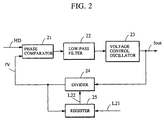
- Fig. 2 is a block diagram of the PLL circuit.
- a horizontal synchronous signal HD serving as a reference, is input to one input terminal of a phase comparator 21, and a signal fV is input to the other input terminal of the phase comparator 21.
- the phase comparator 21 detects a phase difference between these two input signals, and transmits information on this phase difference to a low-pass filter 22, which converts the output of the phase comparator 21 to a DC voltage necessary for a voltage control oscillator 23, and supplies this DC voltage to the voltage control oscillator 23.
- the voltage control oscillator 23 generates a signal f out (dot clock) on the basis of the DC voltage.
- the signal f out output from the voltage control oscillator 23, is divided by a divider 24 on the basis of a value supplied from a register 25, and is fed back to the phase comparator 21 as a signal fV.
- the division value of the register 25, which is set at the outset, is written therein through a signal line L21.
- the division value written in the register 25 is controlled on the basis of the signal fV.
- the logical value of the signal fV is "0"
- the division value in the register 25 is re-written in the divider 24 through a signal line L22.
- the divider 24 divides the output signal f out of the voltage control oscillator 23 by a predetermined division value, and then compares the frequency of the reference signal (the horizontal synchronous signal HD) with the phase frequency to effect locking.
- the frequency of the output signal f out of the voltage control oscillator 23 is locked at a frequency which is obtained by multiplying the frequency of the reference signal (the horizontal synchronous signal HD) by N.
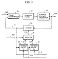
- Fig. 3 is a block diagram of a PLL circuit according to the present invention.
- a control section sets division values T1 and T2 for registers 31 and 32 through signal lines L31 and L32, respectively.
- Output signal lines L33 and L34 of the registers 31 and 32 are connected to a selector 26.
- the selector 26 is a circuit which is operated by a control signal (a vertical synchronous signal VD) in such a way that a signal in the signal line L33 or L34 appears on a signal line L35.
- a control signal a vertical synchronous signal VD
- the division value T1 of the register 31 is output through the signal line L33 and the selector 26 to the signal line L35 and set in the divider 24.
- the division value T2 of the register 32 is selected by the selector 26, and set in the divider 24 through the signal line L34 and the selector 26.
- this circuit has two division values, which are controlled on the basis of a control signal (the vertical synchronous signal VD).
- Fig. 4 is a timing chart of Fig. 3, showing the timing of the switching between the division values T1 and T2.
- the division value T1 of the register 31 is selected by the selector 26, and during the period in which the logical value of the signal fV is "0", its value, that is, the division value T1, is re-loaded.
- the selector 26 selects the division value T2 of the register 32, and, during the period "b", the division value T2 is re-loaded each time the signal level of the signal fV becomes "0" (which occurs three times in Fig. A).
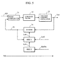
- Figs. 5 and 6 are a block diagram and a timing chart, respectively, of a display control apparatus according to another embodiment of the present invention.
- Symbol HD indicates a reference input signal (a horizontal synchronous signal)
- symbol fV indicates a signal which is obtained by dividing the output of the voltage control oscillator 23 by the divider 24 and which has basically the same frequency as the reference input signal (the horizontal synchronous signal HD).
- a division value (T1) of the contents of a register REG 1 is loaded into the divider 24 through a signal line L40. The loading is effected during the period in which the logical value of the signal fV is "0".
- a second division value in a register REG 2 is loaded into the register REG 1 through a signal line L41.
- the timing of the loading is controlled by a signal LAT output from the control section 17.
- the division value (T2) is loaded into the divider 24 through the signal line L40, and, at the same time, the division value T1 is written to the register REG 2 through a data line DATA from the control section 17.
- this division value T1 causes the division value of the register REG 2 to be shifted to the register REG 1 when the logical value of the control signal (the vertical synchronous signal VD) changes from "0" to "1".
- Fig. 6 is a timing chart of Fig. 5.
- the control section 17 constantly monitors the signal level of the control signal (the vertical synchronous signal VD). When the logical value of the control signal is changed from “1" to "0", the control section 17 generates a signal LAT, and causes the division value T2 in the register REG 2 to be loaded into the register REG 1 through the signal line L41. At the same time, the control section 17 sets the division value T1 to the register REG 2 through the data line DATA.
- this division value T1 is a division value for effecting operation during the period in which the logical value of the control signal (the vertical synchronous signal VD) is "1".
- the PLL circuit operates in a cycle t2
- the logical value of the control signal is "1" it operates in a cycle t1.
- the reference signal has different frequencies, it is possible to avoid an increase in the amount of jitter or an unlocked state due to division values being provided, which respectively correspond to these frequencies, thereby making it possible to operate the system in a stable manner.
Landscapes
- Engineering & Computer Science (AREA)
- Theoretical Computer Science (AREA)
- Physics & Mathematics (AREA)
- Computer Hardware Design (AREA)
- General Physics & Mathematics (AREA)
- Crystallography & Structural Chemistry (AREA)
- Chemical & Material Sciences (AREA)
- Computer Graphics (AREA)
- Control Of Indicators Other Than Cathode Ray Tubes (AREA)
- Stabilization Of Oscillater, Synchronisation, Frequency Synthesizers (AREA)
- Telephone Function (AREA)
- Electrophonic Musical Instruments (AREA)
- Electric Clocks (AREA)
- Controls And Circuits For Display Device (AREA)
- Synchronizing For Television (AREA)
Claims (8)
- Dispositif de commande d'affichage pour générer un signal d'horloge de points pour l'affichage d'un signal vidéo en réponse à un signal de synchronisation, ledit appareil de commande d'affichage comprenant :des moyens de comparaison pour comparer un signal de synchronisation avec un signal multiplié;des moyens générateurs d'horloge pour générer un signal d'horloge de points pour un affichage conformément aux résultats obtenus par lesdits moyens de comparaison;des moyens de stockage pour stocker une valeur de multiplieur dudit signal d'horloge de points pour l'affichage ;des moyens générateurs de signal multiplié pour générer ledit signal multiplié à partir de ladite valeur de multiplieur et dudit signal d'horloge de points pour l'affichage;des moyens de détection pour détecter une variation dudit signal de synchronisation ; etdes moyens de modification pour modifier ladite valeur de multiplieur stockée dans lesdits moyens de stockage lorsqu'une variation dudit signal de synchronisation est détectée par lesdits moyens de détection.
- Dispositif de commande d'affichage selon la revendication 1, dans lequel ledit signal de synchronisation comprend au moins l'un d'un signal de synchronisation horizontale et d'un signal de synchronisation verticale.
- Dispositif de commande d'affichage selon la revendication 2, dans lequel lesdits moyens de détection détectent une variation dudit signal de synchronisation verticale.
- Dispositif de commande d'affichage pour générer un signal d'horloge de points pour l'affichage d'un signal vidéo en réponse à un signal de synchronisation, ledit appareil de commande d'affichage comprenant :des moyens de comparaison pour comparer un signal de synchronisation avec un signal multiplié;des moyens générateurs d'horloge pour générer un signal d'horloge de points pour l'affichage conformément à des résultats obtenus par lesdits moyens de comparaison;des moyens de stockage pour stocker des première et seconde valeurs de multiplieur dudit signal d'horloge de points pour l'affichage ;des moyens générateurs de signal multiplié pour générer ledit signal multiplié à partir desdites valeurs de multiplieur et dudit signal d'horloge de points pour l'affichage ;des moyens de détection pour détecter une variation dudit signal de synchronisation; etdes moyens de sélection pour sélectionner la première ou la seconde valeur de multiplieur stockée dans lesdits moyens de stockage en fonction d'une variation dudit signal de synchronisation détecté par lesdits moyens de détection.
- Dispositif de commande d'affichage selon la revendication 4, dans lequel ledit signal de synchronisation comprend au moins l'un d'un signal de synchronisation horizontale et d'un signal de synchronisation verticale.
- Dispositif de commande d'affichage selon la revendication 5, dans lequel lesdits moyens de détection détectent une variation dudit signal de synchronisation verticale.
- Procédé de commande d'affichage pour générer un signal d'horloge de points en réponse à un signal de synchronisation afin de commander un dispositif d'affichage vidéo, comprenant les étapes qui consistent :à comparer le signal de synchronisation avec un signal multiplié ;à générer un signal d'horloge de points pour l'affichage en réponse à un résultat de ladite comparaison;à stocker une valeur de multiplieur du signal d'horloge de points ;à générer le signal multiplié à partir de la valeur de multiplieur et du signal d'horloge de points ;à détecter une variation du signal de synchronisation ; età modifier la valeur de multiplieur stockée en réponse à une variation détectée du signal de synchronisation.
- Procédé de commande d'affichage pour générer un signal d'horloge de points en réponse à un signal de synchronisation afin de commander un dispositif d'affichage vidéo, comprenant les étapes qui consistent :à comparer le signal de synchronisation avec un signal multiplié;à générer un signal d'horloge de points pour l'affichage en réponse à un résultat de ladite comparaison;à stocker des première et seconde valeurs de multiplieur du signal de points;à générer le signal multiplié à partir des valeurs de multiplieur et du signal d'horloge de points ;à détecter une variation du signal de synchronisation ; età sélectionner la première ou la seconde valeur de multiplieur stockée, en réponse à une variation détectée du signal de synchronisation.
Applications Claiming Priority (2)
| Application Number | Priority Date | Filing Date | Title |
|---|---|---|---|
| JP102750/93 | 1993-04-28 | ||
| JP05102750A JP3109940B2 (ja) | 1993-04-28 | 1993-04-28 | 表示制御装置及び情報処理装置 |
Publications (2)
| Publication Number | Publication Date |
|---|---|
| EP0622775A1 EP0622775A1 (fr) | 1994-11-02 |
| EP0622775B1 true EP0622775B1 (fr) | 1997-09-17 |
Family
ID=14335901
Family Applications (1)
| Application Number | Title | Priority Date | Filing Date |
|---|---|---|---|
| EP94106558A Expired - Lifetime EP0622775B1 (fr) | 1993-04-28 | 1994-04-27 | Dispositif et méthode pour la génération d'horloge pour un dispositif d'affichage |
Country Status (5)
| Country | Link |
|---|---|
| US (1) | US5706035A (fr) |
| EP (1) | EP0622775B1 (fr) |
| JP (1) | JP3109940B2 (fr) |
| AT (1) | ATE158436T1 (fr) |
| DE (1) | DE69405634T2 (fr) |
Families Citing this family (21)
| Publication number | Priority date | Publication date | Assignee | Title |
|---|---|---|---|---|
| JPH07199891A (ja) * | 1993-12-28 | 1995-08-04 | Canon Inc | 表示制御装置 |
| JP3307750B2 (ja) * | 1993-12-28 | 2002-07-24 | キヤノン株式会社 | 表示制御装置 |
| JP3302202B2 (ja) * | 1994-11-10 | 2002-07-15 | キヤノン株式会社 | 表示制御装置 |
| JPH0981074A (ja) * | 1995-09-19 | 1997-03-28 | Fujitsu Ltd | ディスプレイ装置及びディスプレイユニット及びディスプレイ信号生成装置 |
| JP3487119B2 (ja) * | 1996-05-07 | 2004-01-13 | 松下電器産業株式会社 | ドットクロック再生装置 |
| US6067071A (en) * | 1996-06-27 | 2000-05-23 | Cirrus Logic, Inc. | Method and apparatus for expanding graphics images for LCD panels |
| US6389177B1 (en) | 1996-07-02 | 2002-05-14 | Apple Computer, Inc. | System and method using edge processing to remove blocking artifacts from decompressed images |
| US5914764A (en) * | 1996-09-25 | 1999-06-22 | Rockwell International Corporation | Method and apparatus for using optical response time to control a liquid crystal display |
| US5953074A (en) * | 1996-11-18 | 1999-09-14 | Sage, Inc. | Video adapter circuit for detection of analog video scanning formats |
| US6195079B1 (en) | 1996-11-18 | 2001-02-27 | Sage, Inc. | On-screen user interface for a video adapter circuit |
| WO1998023094A2 (fr) * | 1996-11-18 | 1998-05-28 | Sage, Inc. | Circuit d'adaptateur pour moniteur a ecran plat |
| US5907330A (en) * | 1996-12-18 | 1999-05-25 | Intel Corporation | Reducing power consumption and bus bandwidth requirements in cellular phones and PDAS by using a compressed display cache |
| WO1999005666A1 (fr) | 1997-07-25 | 1999-02-04 | Apple Computer, Inc. | Systeme et procede de production de fenetres a luminance elevee sur un dispositif d'affichage d'ordinateur |
| US6175361B1 (en) * | 1997-10-27 | 2001-01-16 | Sony Corporation | Frequency generation during switch-over for multi-frequency video monitor |
| US6313823B1 (en) | 1998-01-20 | 2001-11-06 | Apple Computer, Inc. | System and method for measuring the color output of a computer monitor |
| US6538648B1 (en) * | 1998-04-28 | 2003-03-25 | Sanyo Electric Co., Ltd. | Display device |
| US7412654B1 (en) * | 1998-09-24 | 2008-08-12 | Apple, Inc. | Apparatus and method for handling special windows in a display |
| US6310618B1 (en) * | 1998-11-13 | 2001-10-30 | Smartasic, Inc. | Clock generation for sampling analong video |
| JP2005208992A (ja) * | 2004-01-23 | 2005-08-04 | Canon Inc | 位置情報出力装置及び信号処理方法 |
| JP2008276132A (ja) * | 2007-05-07 | 2008-11-13 | Nec Electronics Corp | ドットクロック発生回路、半導体装置及びドットクロック発生方法 |
| US20090189842A1 (en) * | 2008-01-24 | 2009-07-30 | Industrial Technology Research Institute | Backlight control apparatus |
Family Cites Families (5)
| Publication number | Priority date | Publication date | Assignee | Title |
|---|---|---|---|---|
| US4626837A (en) * | 1983-11-17 | 1986-12-02 | Wyse Technology | Display interface apparatus |
| US4686567A (en) * | 1984-09-28 | 1987-08-11 | Sundstrand Data Control, Inc. | Timing circuit for varying the horizontal format of raster scanned display |
| WO1990000789A1 (fr) * | 1988-07-14 | 1990-01-25 | Seiko Epson Corporation | Circuit de traitement de signaux video |
| JP2531426B2 (ja) * | 1993-02-01 | 1996-09-04 | 日本電気株式会社 | マルチスキャン型液晶ディスプレイ装置 |
| JP2537013B2 (ja) * | 1993-09-30 | 1996-09-25 | インターナショナル・ビジネス・マシーンズ・コーポレイション | 液晶表示装置用のドット・クロック生成装置 |
-
1993
- 1993-04-28 JP JP05102750A patent/JP3109940B2/ja not_active Expired - Fee Related
-
1994
- 1994-04-27 AT AT94106558T patent/ATE158436T1/de not_active IP Right Cessation
- 1994-04-27 DE DE69405634T patent/DE69405634T2/de not_active Expired - Fee Related
- 1994-04-27 EP EP94106558A patent/EP0622775B1/fr not_active Expired - Lifetime
- 1994-04-28 US US08/234,961 patent/US5706035A/en not_active Expired - Lifetime
Also Published As
| Publication number | Publication date |
|---|---|
| JPH06314088A (ja) | 1994-11-08 |
| DE69405634T2 (de) | 1998-02-26 |
| EP0622775A1 (fr) | 1994-11-02 |
| JP3109940B2 (ja) | 2000-11-20 |
| US5706035A (en) | 1998-01-06 |
| ATE158436T1 (de) | 1997-10-15 |
| DE69405634D1 (de) | 1997-10-23 |
Similar Documents
| Publication | Publication Date | Title |
|---|---|---|
| EP0622775B1 (fr) | Dispositif et méthode pour la génération d'horloge pour un dispositif d'affichage | |
| EP0661685B1 (fr) | Appareil pour la génération d'un signal d'horloge pour affichage | |
| US6078317A (en) | Display device, and display control method and apparatus therefor | |
| US6215467B1 (en) | Display control apparatus and method and display apparatus | |
| JP2903044B2 (ja) | ビデオ信号変換器及び方法 | |
| US5917552A (en) | Video signal interface system utilizing deductive control | |
| US6097364A (en) | Display control apparatus which compresses image data to reduce the size of a display memory | |
| US6661414B1 (en) | Display system with a displaying apparatus that transmits control information | |
| EP0725380A1 (fr) | Méthode pour contrÔler un dispositif d'affichage avec fonction pour le maintien de dispositif d'affichage et système pour contrÔler un dispositif d'affichage | |
| JP2950261B2 (ja) | 液晶表示装置 | |
| KR0162529B1 (ko) | 멀티스캔 lcd 용 디스플레이 제어기와 디스플레이 제어방법 | |
| JPH0946619A (ja) | 映像信号処理装置および表示システム | |
| JP3307750B2 (ja) | 表示制御装置 | |
| KR100442002B1 (ko) | 화상표시장치 | |
| US5541646A (en) | Display image stabilization apparatus and method of using same | |
| JP3302202B2 (ja) | 表示制御装置 | |
| EP0316946B1 (fr) | Appareil de signaux de vidéo avec sortie sur support en papier | |
| US7834866B2 (en) | Display panel driver and display panel driving method | |
| US6118440A (en) | Image display system and display control apparatus | |
| JPH0944118A (ja) | インターフェイス回路 | |
| JPH07219486A (ja) | 液晶表示装置 | |
| JPH0962239A (ja) | 表示制御装置及び方法 | |
| JPH06292147A (ja) | 映像信号処理回路 |
Legal Events
| Date | Code | Title | Description |
|---|---|---|---|
| PUAI | Public reference made under article 153(3) epc to a published international application that has entered the european phase |
Free format text: ORIGINAL CODE: 0009012 |
|
| AK | Designated contracting states |
Kind code of ref document: A1 Designated state(s): AT BE CH DE DK ES FR GB GR IE IT LI LU MC NL PT SE |
|
| 17P | Request for examination filed |
Effective date: 19950320 |
|
| GRAG | Despatch of communication of intention to grant |
Free format text: ORIGINAL CODE: EPIDOS AGRA |
|
| 17Q | First examination report despatched |
Effective date: 19961112 |
|
| GRAH | Despatch of communication of intention to grant a patent |
Free format text: ORIGINAL CODE: EPIDOS IGRA |
|
| GRAH | Despatch of communication of intention to grant a patent |
Free format text: ORIGINAL CODE: EPIDOS IGRA |
|
| GRAA | (expected) grant |
Free format text: ORIGINAL CODE: 0009210 |
|
| AK | Designated contracting states |
Kind code of ref document: B1 Designated state(s): AT BE CH DE DK ES FR GB GR IE IT LI LU MC NL PT SE |
|
| PG25 | Lapsed in a contracting state [announced via postgrant information from national office to epo] |
Ref country code: LI Free format text: LAPSE BECAUSE OF FAILURE TO SUBMIT A TRANSLATION OF THE DESCRIPTION OR TO PAY THE FEE WITHIN THE PRESCRIBED TIME-LIMIT Effective date: 19970917 Ref country code: GR Free format text: LAPSE BECAUSE OF FAILURE TO SUBMIT A TRANSLATION OF THE DESCRIPTION OR TO PAY THE FEE WITHIN THE PRESCRIBED TIME-LIMIT Effective date: 19970917 Ref country code: ES Free format text: THE PATENT HAS BEEN ANNULLED BY A DECISION OF A NATIONAL AUTHORITY Effective date: 19970917 Ref country code: DK Free format text: LAPSE BECAUSE OF NON-PAYMENT OF DUE FEES Effective date: 19970917 Ref country code: CH Free format text: LAPSE BECAUSE OF FAILURE TO SUBMIT A TRANSLATION OF THE DESCRIPTION OR TO PAY THE FEE WITHIN THE PRESCRIBED TIME-LIMIT Effective date: 19970917 Ref country code: BE Effective date: 19970917 Ref country code: AT Effective date: 19970917 |
|
| REF | Corresponds to: |
Ref document number: 158436 Country of ref document: AT Date of ref document: 19971015 Kind code of ref document: T |
|
| REG | Reference to a national code |
Ref country code: CH Ref legal event code: EP |
|
| REF | Corresponds to: |
Ref document number: 69405634 Country of ref document: DE Date of ref document: 19971023 |
|
| ET | Fr: translation filed | ||
| ITF | It: translation for a ep patent filed | ||
| PG25 | Lapsed in a contracting state [announced via postgrant information from national office to epo] |
Ref country code: SE Effective date: 19971217 Ref country code: PT Effective date: 19971217 |
|
| REG | Reference to a national code |
Ref country code: IE Ref legal event code: FG4D Free format text: 76521 |
|
| REG | Reference to a national code |
Ref country code: CH Ref legal event code: PL |
|
| PG25 | Lapsed in a contracting state [announced via postgrant information from national office to epo] |
Ref country code: LU Free format text: LAPSE BECAUSE OF NON-PAYMENT OF DUE FEES Effective date: 19980427 Ref country code: IE Free format text: LAPSE BECAUSE OF NON-PAYMENT OF DUE FEES Effective date: 19980427 |
|
| PLBE | No opposition filed within time limit |
Free format text: ORIGINAL CODE: 0009261 |
|
| STAA | Information on the status of an ep patent application or granted ep patent |
Free format text: STATUS: NO OPPOSITION FILED WITHIN TIME LIMIT |
|
| 26N | No opposition filed | ||
| PG25 | Lapsed in a contracting state [announced via postgrant information from national office to epo] |
Ref country code: MC Free format text: LAPSE BECAUSE OF NON-PAYMENT OF DUE FEES Effective date: 19981031 |
|
| REG | Reference to a national code |
Ref country code: GB Ref legal event code: IF02 |
|
| PGFP | Annual fee paid to national office [announced via postgrant information from national office to epo] |
Ref country code: NL Payment date: 20050403 Year of fee payment: 12 |
|
| PGFP | Annual fee paid to national office [announced via postgrant information from national office to epo] |
Ref country code: FR Payment date: 20050408 Year of fee payment: 12 |
|
| PGFP | Annual fee paid to national office [announced via postgrant information from national office to epo] |
Ref country code: DE Payment date: 20050421 Year of fee payment: 12 |
|
| PGFP | Annual fee paid to national office [announced via postgrant information from national office to epo] |
Ref country code: GB Payment date: 20050427 Year of fee payment: 12 |
|
| PG25 | Lapsed in a contracting state [announced via postgrant information from national office to epo] |
Ref country code: GB Free format text: LAPSE BECAUSE OF NON-PAYMENT OF DUE FEES Effective date: 20060427 |
|
| PGFP | Annual fee paid to national office [announced via postgrant information from national office to epo] |
Ref country code: IT Payment date: 20060430 Year of fee payment: 13 |
|
| PG25 | Lapsed in a contracting state [announced via postgrant information from national office to epo] |
Ref country code: NL Free format text: LAPSE BECAUSE OF NON-PAYMENT OF DUE FEES Effective date: 20061101 Ref country code: DE Free format text: LAPSE BECAUSE OF NON-PAYMENT OF DUE FEES Effective date: 20061101 |
|
| GBPC | Gb: european patent ceased through non-payment of renewal fee |
Effective date: 20060427 |
|
| NLV4 | Nl: lapsed or anulled due to non-payment of the annual fee |
Effective date: 20061101 |
|
| REG | Reference to a national code |
Ref country code: FR Ref legal event code: ST Effective date: 20061230 |
|
| PG25 | Lapsed in a contracting state [announced via postgrant information from national office to epo] |
Ref country code: FR Free format text: LAPSE BECAUSE OF NON-PAYMENT OF DUE FEES Effective date: 20060502 |
|
| PG25 | Lapsed in a contracting state [announced via postgrant information from national office to epo] |
Ref country code: IT Free format text: LAPSE BECAUSE OF NON-PAYMENT OF DUE FEES Effective date: 20070427 |