EP0622839A2 - Procédé pour la connexion d'un circuit intégré à un circuit externe - Google Patents
Procédé pour la connexion d'un circuit intégré à un circuit externe Download PDFInfo
- Publication number
- EP0622839A2 EP0622839A2 EP94830204A EP94830204A EP0622839A2 EP 0622839 A2 EP0622839 A2 EP 0622839A2 EP 94830204 A EP94830204 A EP 94830204A EP 94830204 A EP94830204 A EP 94830204A EP 0622839 A2 EP0622839 A2 EP 0622839A2
- Authority
- EP
- European Patent Office
- Prior art keywords
- circuit
- integrated circuit
- external circuit
- process according
- connection
- Prior art date
- Legal status (The legal status is an assumption and is not a legal conclusion. Google has not performed a legal analysis and makes no representation as to the accuracy of the status listed.)
- Withdrawn
Links
Images

Classifications
-
- G—PHYSICS
- G06—COMPUTING OR CALCULATING; COUNTING
- G06F—ELECTRIC DIGITAL DATA PROCESSING
- G06F15/00—Digital computers in general; Data processing equipment in general
- G06F15/02—Digital computers in general; Data processing equipment in general manually operated with input through keyboard and computation using a built-in program, e.g. pocket calculators
- G06F15/0216—Constructional details or arrangements
-
- H—ELECTRICITY
- H01—ELECTRIC ELEMENTS
- H01B—CABLES; CONDUCTORS; INSULATORS; SELECTION OF MATERIALS FOR THEIR CONDUCTIVE, INSULATING OR DIELECTRIC PROPERTIES
- H01B1/00—Conductors or conductive bodies characterised by the conductive materials; Selection of materials as conductors
- H01B1/20—Conductive material dispersed in non-conductive organic material
- H01B1/22—Conductive material dispersed in non-conductive organic material the conductive material comprising metals or alloys
-
- H—ELECTRICITY
- H01—ELECTRIC ELEMENTS
- H01R—ELECTRICALLY-CONDUCTIVE CONNECTIONS; STRUCTURAL ASSOCIATIONS OF A PLURALITY OF MUTUALLY-INSULATED ELECTRICAL CONNECTING ELEMENTS; COUPLING DEVICES; CURRENT COLLECTORS
- H01R12/00—Structural associations of a plurality of mutually-insulated electrical connecting elements, specially adapted for printed circuits, e.g. printed circuit boards [PCB], flat or ribbon cables, or like generally planar structures, e.g. terminal strips, terminal blocks; Coupling devices specially adapted for printed circuits, flat or ribbon cables, or like generally planar structures; Terminals specially adapted for contact with, or insertion into, printed circuits, flat or ribbon cables, or like generally planar structures
- H01R12/50—Fixed connections
- H01R12/59—Fixed connections for flexible printed circuits, flat or ribbon cables or like structures
- H01R12/62—Fixed connections for flexible printed circuits, flat or ribbon cables or like structures connecting to rigid printed circuits or like structures
-
- H—ELECTRICITY
- H01—ELECTRIC ELEMENTS
- H01R—ELECTRICALLY-CONDUCTIVE CONNECTIONS; STRUCTURAL ASSOCIATIONS OF A PLURALITY OF MUTUALLY-INSULATED ELECTRICAL CONNECTING ELEMENTS; COUPLING DEVICES; CURRENT COLLECTORS
- H01R4/00—Electrically-conductive connections between two or more conductive members in direct contact, i.e. touching one another; Means for effecting or maintaining such contact; Electrically-conductive connections having two or more spaced connecting locations for conductors and using contact members penetrating insulation
- H01R4/04—Electrically-conductive connections between two or more conductive members in direct contact, i.e. touching one another; Means for effecting or maintaining such contact; Electrically-conductive connections having two or more spaced connecting locations for conductors and using contact members penetrating insulation using electrically conductive adhesives
-
- H—ELECTRICITY
- H10—SEMICONDUCTOR DEVICES; ELECTRIC SOLID-STATE DEVICES NOT OTHERWISE PROVIDED FOR
- H10W—GENERIC PACKAGES, INTERCONNECTIONS, CONNECTORS OR OTHER CONSTRUCTIONAL DETAILS OF DEVICES COVERED BY CLASS H10
- H10W72/00—Interconnections or connectors in packages
- H10W72/071—Connecting or disconnecting
- H10W72/073—Connecting or disconnecting of die-attach connectors
- H10W72/07331—Connecting techniques
-
- H—ELECTRICITY
- H10—SEMICONDUCTOR DEVICES; ELECTRIC SOLID-STATE DEVICES NOT OTHERWISE PROVIDED FOR
- H10W—GENERIC PACKAGES, INTERCONNECTIONS, CONNECTORS OR OTHER CONSTRUCTIONAL DETAILS OF DEVICES COVERED BY CLASS H10
- H10W72/00—Interconnections or connectors in packages
- H10W72/30—Die-attach connectors
- H10W72/321—Structures or relative sizes of die-attach connectors
- H10W72/325—Die-attach connectors having a filler embedded in a matrix
-
- H—ELECTRICITY
- H10—SEMICONDUCTOR DEVICES; ELECTRIC SOLID-STATE DEVICES NOT OTHERWISE PROVIDED FOR
- H10W—GENERIC PACKAGES, INTERCONNECTIONS, CONNECTORS OR OTHER CONSTRUCTIONAL DETAILS OF DEVICES COVERED BY CLASS H10
- H10W72/00—Interconnections or connectors in packages
- H10W72/30—Die-attach connectors
- H10W72/351—Materials of die-attach connectors
- H10W72/352—Materials of die-attach connectors comprising metals or metalloids, e.g. solders
-
- H—ELECTRICITY
- H10—SEMICONDUCTOR DEVICES; ELECTRIC SOLID-STATE DEVICES NOT OTHERWISE PROVIDED FOR
- H10W—GENERIC PACKAGES, INTERCONNECTIONS, CONNECTORS OR OTHER CONSTRUCTIONAL DETAILS OF DEVICES COVERED BY CLASS H10
- H10W72/00—Interconnections or connectors in packages
- H10W72/30—Die-attach connectors
- H10W72/351—Materials of die-attach connectors
- H10W72/353—Materials of die-attach connectors not comprising solid metals or solid metalloids, e.g. ceramics
- H10W72/354—Materials of die-attach connectors not comprising solid metals or solid metalloids, e.g. ceramics comprising polymers
Definitions
- the invention is included between the microelectronics technologies concerning the packaging of integrated circuits, and still more precisely in the kind of products so-called "consumer products”.
- VLSI circuits are realized integrating hundred thousands of elementary components connected each other in a silicon plate.
- the package realizes a protection of the chip, bringing its electrical connections to a density compatible with the printed circuit, being at the same time realized in such a way that it can be used with the standard fabrication techniques employed in this field (e.g. welding process employing tin/lead alloys melting at about 200°C).
- This kind of package requires the use of a lead-frame sustaining the chip and creating the external contacts of the package, of the wires connecting the chip to the lead-frame, of the plastic resins encasing the connection and giving the desired shape to the package, the adoption of processes like the deposition and the hardening of the alloy fixing the chip to the lead-frame, the welding of the connecting wires, the pressing of the resin to shape the package, the shearing of the terminals (lead frame) and their bending to make them suitable for welding.
- Terminals are then welded by heat compression or eutectic welding on a film upon which the copper circuit lined with tin or gold is laminated.
- This technology is competitive as far as costs and dimensions are concerned, but it can be used only in particular cases in view of the specific requisites.
- C4 the technology known as IBM
- IBM provides the deposition on the integrated circuit preferably of microspheres in correspondence of the connecting connection pads and the consequent re-melting of the same after that the connection pads of the chip have been aligned with those corresponding on the connecting circuit.
- COG Chip On Glass
- a gold or copper bump must be realized by thin film, photolithografic technique and galvanic growing, one bump corresponding to each connection pad of the chip, before making the cut of the single chip from the wafer.
- ITO Indium-Tin oxide
- connection is made. It can also be possible to use, in some cases, anisotropic glues with a polymeric base, conferring a conductivity only along the Z axis, in place of the welding pastes, making also in this case the connection by compression.
- the solution proposed according to the invention is based on the utilization of an anisotropic material, such as a thermoplastic or thermosetting adhesive, in the form of a film or a paste, charged with conductive microspheres, randomly dispersed in the polymeric matrix.
- an anisotropic material such as a thermoplastic or thermosetting adhesive
- said circuit 1 can also be realized employing rigid material, for example glass.
- the metallic particles assure the necessary electric contact, while the thermosetting matrix assure the mechanical features of the connection (figure 2d).
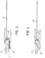
- FIG 4 Another prototype realized on the basis of the above technology is that shown in figure 4, and concerns a calculator on a flexible substrate to be compared with figure 3 in order to appreciate the differences and the results obtained.
- the frequencies used were between 10 KHz and 10 MHz.
Landscapes
- Engineering & Computer Science (AREA)
- Physics & Mathematics (AREA)
- Theoretical Computer Science (AREA)
- Computing Systems (AREA)
- Computer Hardware Design (AREA)
- General Engineering & Computer Science (AREA)
- General Physics & Mathematics (AREA)
- Chemical & Material Sciences (AREA)
- Dispersion Chemistry (AREA)
- Spectroscopy & Molecular Physics (AREA)
- Wire Bonding (AREA)
Applications Claiming Priority (2)
| Application Number | Priority Date | Filing Date | Title |
|---|---|---|---|
| ITRM930273A IT1261464B (it) | 1993-04-30 | 1993-04-30 | Procedimento per la connessione di un circuito integrato ad un circuito esterno. |
| ITRM930273 | 1993-04-30 |
Publications (2)
| Publication Number | Publication Date |
|---|---|
| EP0622839A2 true EP0622839A2 (fr) | 1994-11-02 |
| EP0622839A3 EP0622839A3 (fr) | 1995-03-29 |
Family
ID=11401735
Family Applications (1)
| Application Number | Title | Priority Date | Filing Date |
|---|---|---|---|
| EP94830204A Withdrawn EP0622839A3 (fr) | 1993-04-30 | 1994-04-29 | Procédé pour la connexion d'un circuit intégré à un circuit externe. |
Country Status (2)
| Country | Link |
|---|---|
| EP (1) | EP0622839A3 (fr) |
| IT (1) | IT1261464B (fr) |
Cited By (2)
| Publication number | Priority date | Publication date | Assignee | Title |
|---|---|---|---|---|
| EP0691660A1 (fr) * | 1994-05-10 | 1996-01-10 | Hitachi Chemical Co., Ltd. | Film de résine à électroconduction anisotrope |
| EP0824270A3 (fr) * | 1996-08-06 | 1999-06-09 | Hitachi Chemical Co., Ltd. | Procédé pour le montage d'une pluralité de pièces électroniques sur un panneau de circuit |
Family Cites Families (4)
| Publication number | Priority date | Publication date | Assignee | Title |
|---|---|---|---|---|
| JPS60225438A (ja) * | 1984-04-23 | 1985-11-09 | Seiko Epson Corp | Ic実装構造 |
| JPS62244143A (ja) * | 1986-04-16 | 1987-10-24 | Matsushita Electric Ind Co Ltd | 半導体素子の電気的接続方法 |
| JPH01129431A (ja) * | 1987-11-16 | 1989-05-22 | Sharp Corp | 半導体チップ実装方式 |
| US5123986A (en) * | 1989-08-10 | 1992-06-23 | Casio Computer Co., Ltd. | Conductive connecting method |
-
1993
- 1993-04-30 IT ITRM930273A patent/IT1261464B/it active IP Right Grant
-
1994
- 1994-04-29 EP EP94830204A patent/EP0622839A3/fr not_active Withdrawn
Cited By (7)
| Publication number | Priority date | Publication date | Assignee | Title |
|---|---|---|---|---|
| EP0691660A1 (fr) * | 1994-05-10 | 1996-01-10 | Hitachi Chemical Co., Ltd. | Film de résine à électroconduction anisotrope |
| US6042894A (en) * | 1994-05-10 | 2000-03-28 | Hitachi Chemical Company, Ltd. | Anisotropically electroconductive resin film |
| EP0824270A3 (fr) * | 1996-08-06 | 1999-06-09 | Hitachi Chemical Co., Ltd. | Procédé pour le montage d'une pluralité de pièces électroniques sur un panneau de circuit |
| US6158115A (en) * | 1996-08-06 | 2000-12-12 | Hitachi Chemical Company, Ltd. | Method of mounting a plurality of electronic parts on a circuit board |
| US6479757B1 (en) | 1996-08-06 | 2002-11-12 | Hitachi Chemical Company, Ltd. | Method of mounting a plurality of electronic parts on a circuit board |
| CN1098617C (zh) * | 1996-08-06 | 2003-01-08 | 日立化成工业株式会社 | 电路基板上安装带粘接剂的电子元器件的方法 |
| US6841022B2 (en) | 1996-08-06 | 2005-01-11 | Hitachi Chemical Company, Ltd. | Adhesive-coated electronic parts on a connection sheet |
Also Published As
| Publication number | Publication date |
|---|---|
| ITRM930273A0 (it) | 1993-04-30 |
| ITRM930273A1 (it) | 1994-10-30 |
| EP0622839A3 (fr) | 1995-03-29 |
| IT1261464B (it) | 1996-05-23 |
Similar Documents
| Publication | Publication Date | Title |
|---|---|---|
| US5586892A (en) | Electrically connecting structure | |
| EP0332402B1 (fr) | Disposition de connexion et procédé pour sa fabrication | |
| US5838061A (en) | Semiconductor package including a semiconductor chip adhesively bonded thereto | |
| US5684330A (en) | Chip-sized package having metal circuit substrate | |
| KR100694739B1 (ko) | 다수의 전원/접지면을 갖는 볼 그리드 어레이 패키지 | |
| US6905911B2 (en) | Semiconductor device, method for manufacturing an electronic equipment, electronic equipment, and portable information terminal | |
| US7105931B2 (en) | Electronic package and method | |
| US5561323A (en) | Electronic package with thermally conductive support member having a thin circuitized substrate and semiconductor device bonded thereto | |
| US7575955B2 (en) | Method for making electronic packages | |
| US5773884A (en) | Electronic package with thermally conductive support member having a thin circuitized substrate and semiconductor device bonded thereto | |
| US5633533A (en) | Electronic package with thermally conductive support member having a thin circuitized substrate and semiconductor device bonded thereto | |
| US6081038A (en) | Semiconductor chip package structure | |
| KR20030083553A (ko) | 반도체 장치 및 그 제조 방법 | |
| US5469333A (en) | Electronic package assembly with protective encapsulant material on opposing sides not having conductive leads | |
| US4423435A (en) | Assembly of an electronic device on an insulative substrate | |
| KR20040069962A (ko) | 전자 소자 캐리어를 위한 최적화된 덮개의 장착 | |
| US7229850B2 (en) | Method of making assemblies having stacked semiconductor chips | |
| US6335563B1 (en) | Semiconductor device, method of fabricating the same, circuit board, and electronic device | |
| US6815830B2 (en) | Semiconductor device and method of manufacturing the same, circuit board and electronic instrument | |
| US6593652B2 (en) | Semiconductor device reinforced by a highly elastic member made of a synthetic resin | |
| KR101096330B1 (ko) | 반도체 장치용 패키지 | |
| US20070063347A1 (en) | Packages, anisotropic conductive films, and conductive particles utilized therein | |
| KR100230189B1 (ko) | 볼 그리드 어레이 반도체 패키지 | |
| EP0622839A2 (fr) | Procédé pour la connexion d'un circuit intégré à un circuit externe | |
| KR100510518B1 (ko) | 반도체 장치 및 반도체 장치의 패키지 방법 |
Legal Events
| Date | Code | Title | Description |
|---|---|---|---|
| PUAI | Public reference made under article 153(3) epc to a published international application that has entered the european phase |
Free format text: ORIGINAL CODE: 0009012 |
|
| AK | Designated contracting states |
Kind code of ref document: A2 Designated state(s): AT BE CH DE DK ES FR GB GR IE IT LI LU MC NL PT SE |
|
| PUAL | Search report despatched |
Free format text: ORIGINAL CODE: 0009013 |
|
| AK | Designated contracting states |
Kind code of ref document: A3 Designated state(s): AT BE CH DE DK ES FR GB GR IE IT LI LU MC NL PT SE |
|
| STAA | Information on the status of an ep patent application or granted ep patent |
Free format text: STATUS: THE APPLICATION IS DEEMED TO BE WITHDRAWN |
|
| 18D | Application deemed to be withdrawn |
Effective date: 19950930 |